EP1048956A2 - Method and apparatus for analizing a semiconductor wafer manufacturing process - Google Patents
Method and apparatus for analizing a semiconductor wafer manufacturing process Download PDFInfo
- Publication number
- EP1048956A2 EP1048956A2 EP00303349A EP00303349A EP1048956A2 EP 1048956 A2 EP1048956 A2 EP 1048956A2 EP 00303349 A EP00303349 A EP 00303349A EP 00303349 A EP00303349 A EP 00303349A EP 1048956 A2 EP1048956 A2 EP 1048956A2
- Authority
- EP
- European Patent Office
- Prior art keywords
- memory cells
- yield
- wafer
- defects
- detected
- Prior art date
- Legal status (The legal status is an assumption and is not a legal conclusion. Google has not performed a legal analysis and makes no representation as to the accuracy of the status listed.)
- Withdrawn
Links
Images


Classifications
-
- H—ELECTRICITY
- H10—SEMICONDUCTOR DEVICES; ELECTRIC SOLID-STATE DEVICES NOT OTHERWISE PROVIDED FOR
- H10P—GENERIC PROCESSES OR APPARATUS FOR THE MANUFACTURE OR TREATMENT OF DEVICES COVERED BY CLASS H10
- H10P74/00—Testing or measuring during manufacture or treatment of wafers, substrates or devices
- H10P74/23—Testing or measuring during manufacture or treatment of wafers, substrates or devices characterised by multiple measurements, corrections, marking or sorting processes
Definitions
- the present invention relates to the field of semiconductor wafer processing, and, more particularly, to a method and apparatus for analyzing a semiconductor wafer process for increasing the yield of semiconductor wafers.
- Semiconductor wafer processing involves complex process steps to form devices on the surface of a silicon wafer.
- a goal of semiconductor wafer processing is to attain a high yield. Yield is a percentage which indicates the amount of good devices in a wafer divided by the total number of devices in that wafer.
- a number of discrete process steps are required to form a device including an array of memory cells from raw semiconductor material.
- the starting substrate is usually a slice of single crystal silicon referred to as the wafer.
- a plurality of devices are fabricated together in batches of wafers called lots or runs. The individual wafers in a lot may go through individual process steps one at a time or as a batch. At the completion of the process steps, the devices are tested to determine circuit functionality.
- a method of analyzing a failure in a device comprising an array of memory cells is done by testing an electrical property of each memory cell.
- a tester is used to test each memory cell, and the resultant data is provided in a coordinate space of rows (X) and columns (Y) to produce a failure pattern.
- This pattern is generally called a bitmap failure, and corresponds to the cause of the failures.
- the bitmap may also be referred to as a map of failed memory cells.
- a cause of the failure is estimated using the bitmap.
- the cause of the failure obtained with the bitmap is an estimation of the failure and an electrical abnormality at that position, i.e., an estimation of what failure is happening at which position. Failures may be a result of particle contamination, leakages, opens or shorts resulting during an individual process step.
- the cause of a failure is not always located at the position of the failure found by the tester, and there are many cases where the cause of a failure is located at a position other than the position of the failure. Moreover, not all the foreign materials and defects produced during the manufacturing process cause a failure, and whether foreign materials or defects cause a failure or not depends on the position, size and the like thereof. Therefore, there is a need to improve the way defects are analyzed during a semiconductor wafer process.
- a method for processing semiconductor wafers comprising the step of performing process steps to make at least one wafer comprising a plurality of devices with each device comprising an array of memory cells.
- Each array of memory cells are preferably inspected to detect defects.
- Failed memory cells are preferably predicted based upon detected defects, and a yield of the wafer is preferably predicted based upon the predicted failed memory cells. The predicted yield is preferably compared to a threshold to determine if corrective action is needed.
- yield prediction of the wafer being processed is preferably done in two steps. First, the probability of a detected defect resulting in a failed memory cell is preferably predicted. Second, this predicted probability is preferably used to predict the yield of the wafer being processed. Accurately predicting the probability of a detected defect resulting in a failed memory cell is necessary for accurately predicting the yield of the wafer.
- the yield of the wafer can be determined accurately without having to analyze areas outside of the array of memory cells.
- the step of predicting failed memory cells preferably comprises comparing detected defects to a database of mapped defect information.
- the database of mapped defect information is preferably being based upon a correlation of defects and associated failed memory cells.
- the method preferably further includes the step of creating the database of mapped defect information. This correlation of data between the defects and failed memory cells provides a relationship between manufacturing processes and failed memory cells in an array of memory cells, which helps to provide faster identification to the process steps contributing to yield losses. This method according to the present invention also improves failure analysis efficiency and accelerates the resolution of yield problems.
- Each array of memory cells are preferably formed in successive layers, and wherein inspecting preferably comprises inspecting each layer.
- the database of mapped defect information is preferably based upon size ranges of detected defects and the associated layer.
- Predicting failed memory cells preferably comprises determining a detected defect size range of each detected defect in an associated layer, and predicting failed memory cells preferably based upon matching the detected defect size range and associated layer with the database of mapped defect information.
- the step of predicting the yield preferably further comprises determining a number of detected defects within each size range and associated layer, and using the predicted failed memory cells and number of detected defects within each size range and associated layer to predict the yield.
- Each array of memory cells preferably forms a random access memory, which may be part of a stand alone memory device, such as a DRAM or SRAM, or the random access memory may be an embedded memory within a digital signal processor, for example.
- the yield prediction apparatus preferably includes a defect inspection device for detecting defects in a wafer comprising a plurality of devices with each device comprising an array of memory cells.
- the yield prediction apparatus preferably further includes a processor for predicting failed memory cells based upon detected defects, and for predicting a yield of the wafer based upon the predicted failed memory cells so that the predicted yield can be compared to a threshold to determine if corrective action is needed.
- the wafer yield prediction apparatus preferably further includes a memory connected to the processor for storing a database of mapped defect information.
- the database of mapped defect information is preferably based upon a correlation of defects and associated failed memory cells.
- the processor preferably predicts failed memory cells by comparing detected defects to the database of mapped defect information.
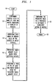
- FIGS. 1-5 A method for processing semiconductor wafers in accordance with the present invention is now described with reference to FIGS. 1-5.
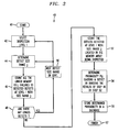
- process steps are performed at Block 12 to make at least one wafer 30 comprising a plurality of devices 32a-32n (FIG. 2).
- Each device generally represented by reference 32 , comprises an array of memory cells.
- the array of memory cells are arranged in a matrix of rows and columns to define a random access memory.
- the random access memory may be part of a DRAM or SRAM, as readily appreciated by one skilled in the art.
- the random access memory may be embedded in the device, with the device being a digital signal processor (DSP), for example.
- DSP digital signal processor
- the process steps are performed in a processing chamber 34 , as best shown in FIG. 2.
- a production flow of the wafer 30 includes process steps A and B being formed in the processing chamber 34 , with a defect inspection device 36 being used between the process steps for inspecting the surface of each device 32 .
- Process step A may be used to form a metal layer for each device 32
- process step B may be used to form a dielectric layer over the metal layer, for example.
- the defect inspection device 36 optically inspects the external appearance of the array of memory cells between the process steps A and B for particle contamination, opens, shots, and the like that may have been introduced as a result of process step A.
- process step A may include defective photolithography or etching.
- the x-y coordinates for each detected defect are stored in a memory 38 .
- This memory 38 is connected to a processor 39 , which may be part of a wafer yield prediction apparatus 39 .
- the wafer yield prediction apparatus 39 will be described in greater detail below.
- Failed memory cells are predicted at Block 16 (FIG. 1) based upon the detected defects, and a yield of the wafer 30 based upon the predicted failed memory cells is predicted at Block 18 using the wafer yield prediction apparatus 37 .
- the predicted yield is compared to a threshold at Block 20 to determine if corrective action is needed.
- the yield prediction is done in two steps. First, the probability of a detected defect resulting in a failed memory cell is predicted. Second, this predicted probability is used to predict the yield of the wafer 30 being processed.
- a second distinction is that the output of the standard prediction algorithm is directly the number of failed devices 32 on the wafer 30 .
- the output of the disclosed prediction algorithm is directly the number of devices 32 with memory cell failures in the wafer 30 .
- the yield of the wafer 30 according to the present invention is then predicted using the correlation between memory failures and detected defects.
- a third distinction is that the standard prediction algorithm uses information of defects detected in the entire device 32 , whereas the disclosed prediction algorithm is computed using information from defects detected just in the array of memory cells. This distinction is particularly advantageous since there is a direct relationship between failed memory cells and a failed device, as readily appreciated by one skilled in the art.
- the probability of a detected defect resulting in a failed memory cell for the standard prediction algorithm is computed for many wafers in several lots to obtain a statistical distribution of the predicted probability.
- the median or mean of the distribution is used in the calculations in the standard yield prediction algorithm.
- the median or mean and confidence intervals i.e., defect size ranges, are used in the disclosed yield prediction algorithm.
- the yield of a particular wafer according to the present invention is based on more than a single number.
- An advantage of the disclosed prediction algorithm is that the probability of a detected defect resulting in a failed memory cell is more accurate since the determination of this probability is made using information provided from a limited portion of the device, i.e., the array of memory cells. There is a statistical relationship between defects detected within the array of memory cells and actual failed memory cells since the memory array area is a regular and dense structure. Consequently, the probability calculated for the memory area is less prone to show dispersions than calculating the probability of the entire device 32 failing.
- the disclosed prediction algorithm thus provides a more accurate result than the standard prediction algorithm because of the above noted distinctions.
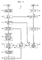
- an initial inspection level i in process step A is selected at Block 42 , and a defect size range j of the detected defect is determined at Block 44 .
- a defect size range j of the detected defect is determined at Block 44 .
- N_linked-failures all the memory cell failures linked to the detected defect at the selected level i with the selected defect size range j are counted (N_linked-failures).
- steps 42 and/or 44 are repeated for the next defect size range or inspection level as selected at Block 50 .
- the defects at the initially selected inspection level i with the selected defect size range j are counted (N_defects) at Block 52 .
- the probability P ij of the detected defect resulting in a failed memory cell is determined at Block 54 by dividing the results of Block 46 (N_linked-failures) by the results of Block 52 (N_defects).
- the determined probability is stored in a database at Block 56 , and the defect prediction algorithm is finished at Block 57
- the database is formed by correlating defect information and failed memory cell location obtained from a lot of processed wafers, generally represented by reference 31 . This lot of wafers does not include the wafer 30 processed in FIG. 2.
- the defect inspection device 36 inspects the surface of the wafers 31 for defects. Electrical tester 62 uses electrical signals to determine which memory cells have failed. The electrical tester 62 is used after the process steps have been completed.
- a correlation device 70 includes a processor 71 for receiving the x-y coordinates of the detected defects from the defect inspection device 36 , as well as for receiving the x-y coordinates of the failed memory cells from the electrical tester 62 .
- the correlated data forming the database of mapped defects is stored in a memory 72 connected to the processor 71 .
- the yield prediction algorithm 74 for predicting the yield of the wafer 30 based upon the predicted failed memory cells will now be described with reference to FIG. 5.
- the yield prediction algorithm 74 provides an estimation of the final yield, i.e., after the devices 32 have been completed and tested, based on information obtained during the process steps. This information is related to defects detected at the inspection points strategically placed along the production flow.
- the yield prediction algorithm 73 may be used to predict the yield on single wafers, as illustrated herein.
- a device 32a within the processed wafer 30 is selected at Block 75 .
- the number of detected defects and the probability of the device failing are initially set to 0.
- the inspection level i and the defect size range j are initially selected at Blocks 77 and 78 .
- the first inspection level i may be selected and the smallest defect size range j may be selected.
- the detected defects at inspection level i (not detected in previous inspections) with defect size range j located within the memory array are counted (N+_ defects). This number is based on actual data from the device 32a being processed.
- the probability P ij of the detected defect causing a memory cell to fail is retrieved at Block 84 .
- This probability P ij was stored in a database at Block 56 as illustrated in FIG. 3.
- the resulting probability P of the device to fail is determined by multiplying P ij times the number of defects counted (N+_defects), and by taking into consideration (Pc) if there are multiple defects in the same memory area at Block 86 .
- the remaining defect size ranges for the selected device 32a are incremented at Block 88 so that other defects detected at inspection level i are counted. Blocks 78-86 are repeated for the remaining defect size ranges. At Block 90 , the additional inspection levels i are taken into consideration by repeating steps 76-86 for the defects detected at the next inspection level i-1 .
- a determination is made if there are more devices on the wafer that provided defect information which needs to be taken into consideration for the wafer yield prediction at Block 94 . If so, then steps 74-90 are repeated for the next device. For each device providing information, N f(P ij , N ij ) is updated at Block 92 . This yield prediction algorithm is finished at Block 96 .
- the wafer yield prediction apparatus 37 includes a processor 39 for predicting failed memory cells in a device 32 on the wafer 30 based upon detected defects therein, and for predicting a yield of the wafer based upon the predicted failed memory cells so that the predicted yield can be compared to a threshold to determine if corrective action is needed.
- the wafer yield prediction apparatus 37 further includes a memory 38 connected to the processor 39 for storing a database of mapped defect information.
- the database of mapped defect information is based upon a correlation of defects and associated failed memory cells.
- the processor 39 predicts failed memory cells by comparing detected defects to the database of mapped defect information.
- the wafer yield prediction apparatus 37 may be part of the defect inspection device 36 , or a standalone apparatus as shown in FIG. 2.
- the memory cells are processed in successive layers, and the defect inspection device 36 inspects each layer.
- the database of mapped defect information is based upon size ranges of detected defects and the associated layer so that the failed memory cells are predicted by the processor 39 by initially determining a detected defect size range of each detected defect in an associated layer.
- the processor 39 predicts failed memory cells based upon matching the detected defect size range and associated layer with the database of mapped defect information.
- the processor 39 is programmed to predict the yield by determining a number of detected defects within each size range and associated layer, and using the predicted failed memory cells and number of detected defects within each size range and associated layer to predict the yield.
- the memory cells form a random access memory, or may be part of an embedded memory, as readily appreciated by one skilled in the art.
Landscapes
- Testing Or Measuring Of Semiconductors Or The Like (AREA)
- For Increasing The Reliability Of Semiconductor Memories (AREA)
Abstract
Description
Claims (17)
- A method for processing semiconductor wafers comprising:performing process steps to make at least one wafer comprising a plurality of devices with each device comprising an array of memory cells;inspecting each array of memory cells to detect defects;predicting failed memory cells based upon detected defects;predicting a yield of the at least one wafer based upon the predicted failed memory cells; andcomparing the predicted yield to a threshold to determine if corrective action is needed.
- A method for processing semiconductor wafers comprising:performing process steps to make at least one wafer comprising a plurality of devices with each device comprising an array of memory cells;inspecting each array of memory cells to detect defects;predicting failed memory cells based upon detected defects by comparing detected defects to a database of mapped defect information, the database of mapped defect information being based upon a correlation of defects and associated failed memory cells; andpredicting a yield of the at least one wafer based upon the predicted failed memory cells.
- A method according to claim 2 further comprising comparing the predicted yield to a threshold to determine if corrective action is needed.
- A method according to claim 2 or claim 3 further comprising creating the database of mapped defect information.
- A method according to claim 2 or claim 3 wherein performing the process steps comprises forming each array of memory cells in successive layers; and wherein inspecting comprises inspecting each layer.
- A method according to claim 5 wherein the database of mapped defect information is based upon size ranges of detected defects and the associated layer; and wherein predicting failed memory cells comprises:determining a detected defect size range of each detected defect in an associated layer; andpredicting failed memory cells based upon matching the detected defect size range and associated layer with the database of mapped defect information.
- A method according to claim 6 wherein predicting the yield further comprises:determining a number of detected defects within each size range and associated layer; andusing the predicted failed memory cells and number of detected defects within each size range and associated layer to predict the yield.
- A method according to claim 1 or claim 2 wherein each array of memory cells forms a random access memory.
- A method according to claim 1 or claim 2 wherein each device comprises the array of memory cells as an embedded memory.
- A method according to claim 1 or claim 2 wherein inspecting comprises optically inspecting.
- A wafer yield prediction apparatus comprising:a defect inspection device for detecting defects in a wafer comprising a plurality of devices with each device comprising an array of memory cells; anda processor for predicting failed memory cells based upon detected defects, and for predicting a yield of the wafer based upon the predicted failed memory cells so that the predicted yield can be compared to a threshold to determine if corrective action is needed.
- A wafer yield prediction apparatus according to Claim 11 further comprising a memory connected to said processor for storing a database of mapped defect information, the database of mapped defect information is based upon a correlation of defects and associated failed memory cells.
- A wafer yield prediction apparatus according to Claim 12 wherein said processor predicts failed memory cells by comparing detected defects to the database of mapped defect information.
- A wafer yield prediction apparatus according to Claim 11 wherein said defect inspection device optically inspects the memory cells.
- A wafer yield prediction apparatus according to Claim 11 wherein the memory cells are processed in successive layers; and wherein said defect inspection device inspects each layer.
- A wafer yield prediction apparatus according to Claim 15 wherein the database of mapped defect information is based upon size ranges of detected defects and the associated layer; and wherein predicting failed memory cells by said processor comprises:determining a detected defect size range of each detected defect in an associated layer; andpredicting failed memory cells based upon matching the detected defect size range and associated layer with the database of mapped defect information.
- A wafer yield prediction apparatus according to Claim 16 wherein said processor predicts the yield by:determining a number of detected defects within each size range and associated layer; andusing the predicted failed memory cells and number of detected defects within each size range and associated layer to predict the yield.
Applications Claiming Priority (5)
| Application Number | Priority Date | Filing Date | Title |
|---|---|---|---|
| US547295 | 1983-10-31 | ||
| 1998-05-21 | |||
| US13147499P | 1999-04-28 | 1999-04-28 | |
| US131474P | 1999-04-28 | ||
| US54729500A | 2000-04-11 | 2000-04-11 |
Publications (2)
| Publication Number | Publication Date |
|---|---|
| EP1048956A2 true EP1048956A2 (en) | 2000-11-02 |
| EP1048956A3 EP1048956A3 (en) | 2003-05-07 |
Family
ID=26829509
Family Applications (1)
| Application Number | Title | Priority Date | Filing Date |
|---|---|---|---|
| EP00303349A Withdrawn EP1048956A3 (en) | 1999-04-28 | 2000-04-20 | Method and apparatus for analizing a semiconductor wafer manufacturing process |
Country Status (1)
| Country | Link |
|---|---|
| EP (1) | EP1048956A3 (en) |
Cited By (6)
| Publication number | Priority date | Publication date | Assignee | Title |
|---|---|---|---|---|
| WO2004025313A1 (en) * | 2002-09-13 | 2004-03-25 | Koninklijke Philips Electronics N.V. | Reduced chip testing scheme at wafer level |
| CN103163442A (en) * | 2013-03-22 | 2013-06-19 | 无锡中星微电子有限公司 | Wafer test method |
| US10318700B2 (en) | 2017-09-05 | 2019-06-11 | International Business Machines Corporation | Modifying a manufacturing process of integrated circuits based on large scale quality performance prediction and optimization |
| CN111814116A (en) * | 2020-07-13 | 2020-10-23 | 全芯智造技术有限公司 | Method and apparatus and computer readable medium for analyzing wafer failure indicators |
| CN116092962A (en) * | 2022-12-09 | 2023-05-09 | 上海华虹宏力半导体制造有限公司 | Yield detection model, acquisition method thereof and method for detecting yield distribution |
| WO2024000731A1 (en) * | 2022-06-27 | 2024-01-04 | 长鑫存储技术有限公司 | Wafer defect evaluation method and apparatus, memory chip, and readable storage medium |
Family Cites Families (3)
| Publication number | Priority date | Publication date | Assignee | Title |
|---|---|---|---|---|
| JP3639636B2 (en) * | 1995-04-25 | 2005-04-20 | 株式会社ルネサステクノロジ | Semiconductor wafer failure analysis apparatus and failure analysis method |
| US5777901A (en) * | 1995-09-29 | 1998-07-07 | Advanced Micro Devices, Inc. | Method and system for automated die yield prediction in semiconductor manufacturing |
| JP3588531B2 (en) * | 1997-03-24 | 2004-11-10 | 株式会社ルネサステクノロジ | Failure analysis device |
-
2000
- 2000-04-20 EP EP00303349A patent/EP1048956A3/en not_active Withdrawn
Cited By (11)
| Publication number | Priority date | Publication date | Assignee | Title |
|---|---|---|---|---|
| WO2004025313A1 (en) * | 2002-09-13 | 2004-03-25 | Koninklijke Philips Electronics N.V. | Reduced chip testing scheme at wafer level |
| US7218093B2 (en) | 2002-09-13 | 2007-05-15 | Nxp B.V. | Reduced chip testing scheme at wafer level |
| CN100390554C (en) * | 2002-09-13 | 2008-05-28 | Nxp股份有限公司 | Chip test solution reduced at wafer level |
| CN103163442A (en) * | 2013-03-22 | 2013-06-19 | 无锡中星微电子有限公司 | Wafer test method |
| CN103163442B (en) * | 2013-03-22 | 2015-05-27 | 无锡中星微电子有限公司 | Wafer test method |
| US10318700B2 (en) | 2017-09-05 | 2019-06-11 | International Business Machines Corporation | Modifying a manufacturing process of integrated circuits based on large scale quality performance prediction and optimization |
| US10810345B2 (en) | 2017-09-05 | 2020-10-20 | International Business Machines Corporation | Modifying a manufacturing process of integrated circuits based on large scale quality performance prediction and optimization |
| CN111814116A (en) * | 2020-07-13 | 2020-10-23 | 全芯智造技术有限公司 | Method and apparatus and computer readable medium for analyzing wafer failure indicators |
| CN111814116B (en) * | 2020-07-13 | 2024-03-26 | 全芯智造技术有限公司 | Method and apparatus for analyzing wafer failure index and computer readable medium |
| WO2024000731A1 (en) * | 2022-06-27 | 2024-01-04 | 长鑫存储技术有限公司 | Wafer defect evaluation method and apparatus, memory chip, and readable storage medium |
| CN116092962A (en) * | 2022-12-09 | 2023-05-09 | 上海华虹宏力半导体制造有限公司 | Yield detection model, acquisition method thereof and method for detecting yield distribution |
Also Published As
| Publication number | Publication date |
|---|---|
| EP1048956A3 (en) | 2003-05-07 |
Similar Documents
| Publication | Publication Date | Title |
|---|---|---|
| US6341241B1 (en) | Defect analysis method and process control method | |
| US6613593B2 (en) | Method of fabricating a semiconductor device | |
| JP5460662B2 (en) | Region determination device, observation device or inspection device, region determination method, and observation method or inspection method using region determination method | |
| US6393602B1 (en) | Method of a comprehensive sequential analysis of the yield losses of semiconductor wafers | |
| KR102546453B1 (en) | Methods and Systems for Inline Component Average Testing and Latent Reliability Defect Detection | |
| KR101448971B1 (en) | Computer-implemented methods for determining if actual defects are potentially systematic defects or potentially random defects | |
| US20030054573A1 (en) | Method for manufacturing semiconductor devices and method and its apparatus for processing detected defect data | |
| CN101459095B (en) | Wafer on-line detection method and on-line detection device | |
| KR20110010690A (en) | Systems and methods for detecting defects on a wafer and generating inspection results for the wafer | |
| US12062166B2 (en) | Method and system for diagnosing a semiconductor wafer | |
| TW202217274A (en) | Identification of an array in a semiconductor specimen | |
| US7982155B2 (en) | System of testing semiconductor devices, a method for testing semiconductor devices, and a method for manufacturing semiconductor devices | |
| US6539272B1 (en) | Electric device inspection method and electric device inspection system | |
| JP2005236094A (en) | Method for manufacturing semiconductor device, method and system for failure analysis | |
| US7035770B2 (en) | Fuzzy reasoning model for semiconductor process fault detection using wafer acceptance test data | |
| US6943569B1 (en) | Method, system and apparatus to detect defects in semiconductor devices | |
| JP4866263B2 (en) | Electronic device quality control method and electronic device quality control system | |
| KR20240130651A (en) | Machine learning based yield prediction | |
| JP4538205B2 (en) | Inspection data analysis program, inspection data analyzer | |
| JP2004525499A (en) | Correction of overlay offset between test layers in integrated circuits | |
| EP1056127A2 (en) | Method and apparatus for correlating data from a semiconductor wafer process | |
| US20250052808A1 (en) | Wafer analyzing device and wafer analyzing system | |
| JP2000252341A (en) | Semiconductor defect analysis system and method | |
| CN117313940A (en) | Method and device for determining wafer yield by using noise network model | |
| WO2025115081A1 (en) | Process diagnosing system, process monitoring system, and wafer |
Legal Events
| Date | Code | Title | Description |
|---|---|---|---|
| PUAI | Public reference made under article 153(3) epc to a published international application that has entered the european phase |
Free format text: ORIGINAL CODE: 0009012 |
|
| AK | Designated contracting states |
Kind code of ref document: A2 Designated state(s): AT BE CH CY DE DK ES FI FR GB GR IE IT LI LU MC NL PT SE |
|
| AX | Request for extension of the european patent |
Free format text: AL;LT;LV;MK;RO;SI |
|
| PUAL | Search report despatched |
Free format text: ORIGINAL CODE: 0009013 |
|
| STAA | Information on the status of an ep patent application or granted ep patent |
Free format text: STATUS: THE APPLICATION IS DEEMED TO BE WITHDRAWN |
|
| AK | Designated contracting states |
Designated state(s): AT BE CH CY DE DK ES FI FR GB GR IE IT LI LU MC NL PT SE |
|
| AX | Request for extension of the european patent |
Extension state: AL LT LV MK RO SI |
|
| RIC1 | Information provided on ipc code assigned before grant |
Ipc: 7H 01L 21/66 B Ipc: 7G 01R 31/28 A |
|
| 18D | Application deemed to be withdrawn |
Effective date: 20021105 |