EP1047178B1 - Resonant DC-to-DC converter and method of controlling the same - Google Patents
Resonant DC-to-DC converter and method of controlling the same Download PDFInfo
- Publication number
- EP1047178B1 EP1047178B1 EP00108751A EP00108751A EP1047178B1 EP 1047178 B1 EP1047178 B1 EP 1047178B1 EP 00108751 A EP00108751 A EP 00108751A EP 00108751 A EP00108751 A EP 00108751A EP 1047178 B1 EP1047178 B1 EP 1047178B1
- Authority
- EP
- European Patent Office
- Prior art keywords
- voltage
- converter
- resonant
- transition
- level signal
- Prior art date
- Legal status (The legal status is an assumption and is not a legal conclusion. Google has not performed a legal analysis and makes no representation as to the accuracy of the status listed.)
- Expired - Lifetime
Links
Images

Classifications
-
- H—ELECTRICITY
- H02—GENERATION; CONVERSION OR DISTRIBUTION OF ELECTRIC POWER
- H02M—APPARATUS FOR CONVERSION BETWEEN AC AND AC, BETWEEN AC AND DC, OR BETWEEN DC AND DC, AND FOR USE WITH MAINS OR SIMILAR POWER SUPPLY SYSTEMS; CONVERSION OF DC OR AC INPUT POWER INTO SURGE OUTPUT POWER; CONTROL OR REGULATION THEREOF
- H02M3/00—Conversion of DC power input into DC power output
- H02M3/22—Conversion of DC power input into DC power output with intermediate conversion into AC
- H02M3/24—Conversion of DC power input into DC power output with intermediate conversion into AC by static converters
- H02M3/28—Conversion of DC power input into DC power output with intermediate conversion into AC by static converters using discharge tubes with control electrode or semiconductor devices with control electrode to produce the intermediate AC
- H02M3/325—Conversion of DC power input into DC power output with intermediate conversion into AC by static converters using discharge tubes with control electrode or semiconductor devices with control electrode to produce the intermediate AC using devices of a triode or a transistor type requiring continuous application of a control signal
- H02M3/335—Conversion of DC power input into DC power output with intermediate conversion into AC by static converters using discharge tubes with control electrode or semiconductor devices with control electrode to produce the intermediate AC using devices of a triode or a transistor type requiring continuous application of a control signal using semiconductor devices only
- H02M3/33561—Conversion of DC power input into DC power output with intermediate conversion into AC by static converters using discharge tubes with control electrode or semiconductor devices with control electrode to produce the intermediate AC using devices of a triode or a transistor type requiring continuous application of a control signal using semiconductor devices only having more than one ouput with independent control
-
- H—ELECTRICITY
- H02—GENERATION; CONVERSION OR DISTRIBUTION OF ELECTRIC POWER
- H02M—APPARATUS FOR CONVERSION BETWEEN AC AND AC, BETWEEN AC AND DC, OR BETWEEN DC AND DC, AND FOR USE WITH MAINS OR SIMILAR POWER SUPPLY SYSTEMS; CONVERSION OF DC OR AC INPUT POWER INTO SURGE OUTPUT POWER; CONTROL OR REGULATION THEREOF
- H02M3/00—Conversion of DC power input into DC power output
- H02M3/22—Conversion of DC power input into DC power output with intermediate conversion into AC
- H02M3/24—Conversion of DC power input into DC power output with intermediate conversion into AC by static converters
- H02M3/28—Conversion of DC power input into DC power output with intermediate conversion into AC by static converters using discharge tubes with control electrode or semiconductor devices with control electrode to produce the intermediate AC
- H02M3/325—Conversion of DC power input into DC power output with intermediate conversion into AC by static converters using discharge tubes with control electrode or semiconductor devices with control electrode to produce the intermediate AC using devices of a triode or a transistor type requiring continuous application of a control signal
- H02M3/335—Conversion of DC power input into DC power output with intermediate conversion into AC by static converters using discharge tubes with control electrode or semiconductor devices with control electrode to produce the intermediate AC using devices of a triode or a transistor type requiring continuous application of a control signal using semiconductor devices only
-
- Y—GENERAL TAGGING OF NEW TECHNOLOGICAL DEVELOPMENTS; GENERAL TAGGING OF CROSS-SECTIONAL TECHNOLOGIES SPANNING OVER SEVERAL SECTIONS OF THE IPC; TECHNICAL SUBJECTS COVERED BY FORMER USPC CROSS-REFERENCE ART COLLECTIONS [XRACs] AND DIGESTS
- Y02—TECHNOLOGIES OR APPLICATIONS FOR MITIGATION OR ADAPTATION AGAINST CLIMATE CHANGE
- Y02B—CLIMATE CHANGE MITIGATION TECHNOLOGIES RELATED TO BUILDINGS, e.g. HOUSING, HOUSE APPLIANCES OR RELATED END-USER APPLICATIONS
- Y02B70/00—Technologies for an efficient end-user side electric power management and consumption
- Y02B70/10—Technologies improving the efficiency by using switched-mode power supplies [SMPS], i.e. efficient power electronics conversion e.g. power factor correction or reduction of losses in power supplies or efficient standby modes
Definitions
- the present invention relates to a resonant-transition dc-to-dc converter, and to a method of controlling the resonant transition of a dc-to-dc converter.
- the present invention may be used to advantage, though not exclusively, in flyback and boost resonant-transition dc-to-dc converters, to which the following description refers purely by way of example.
- circuits comprising linear power supplies, i.e. in which the transistors operate permanently in the linear region.
- One proposed solution is to use supply circuits comprising switching dc-to-dc converters featuring inductive components, the charging and discharging of which are controlled by active components defined by control transistors switching between a saturation and a cutoff condition (on/off).
- switching losses - In switching dc-to-dc converters, the power dissipated during switching - also known as switching losses - is directly proportional to the switching frequency of the active components, which therefore cannot be so high as to result in switching losses making the use of such power supply circuits unfeasible.
- This technique also calls for a discharge circuit to discharge the capacitive element completely when the control transistor is cut off, so that, the instant the control transistor switches to the saturation state, the voltage at its terminals is substantially zero and the switching losses therefore greatly reduced. More detailed information about the Snubber technique is also to be found, for example, in the text mentioned above.
- control transistors for charging and discharging the inductive and capacitive components are turned on or off when the current flowing in them or the voltage at their terminals is zero respectively.
- All known resonant-transition dc-to-dc converters have the drawback of having fairly complex circuit structures and employing a large number of additional components for detecting zero current flow in, or zero voltage at the terminals of, the control transistors.
- US-A-5 680 034 discloses a pulse width modulated (PWM) controller for resonant converters, which controls a zero-voltage switching resonant power converter or inverter.
- PWM pulse width modulated
- the on time of the power switch of the converter or inverter is varied by an error amplifier such that the output voltage of the converter or inverter maintains proportionality to a reference voltage.
- the off time is terminated by a switch-voltage detector when the voltage across the power switch (110) drops below a threshold voltage due to the natural resonance of the external resonating capacitor and inductors.
- a single timing capacitor is employed both for determining the on time and the off time.
- two timing capacitors are employed for separately determining the maximum allowed off time and the variable on time.
- a cycle-by-cycle current limit circuit comprising a current sensor, a comparator, and an R-S latch may be added to the circuits representing each of the embodiments.
- a soft start subcircuit and an overlap detector protection against overdissipation of the power switch caused by loss of zero-voltage switching can also be implemented.
- the soft start subcircuit can also be triggered by a voltage detector, which monitors the output voltage of the power converter or some other voltage within the system, such as the peak voltage across the power switch (110), to effectively implement overvoltage protection.
- the present invention is based on the principle of only switching the control transistor from the cutoff to the saturation condition when the Snubber capacitor is discharged naturally and the voltage at its terminals is therefore substantially zero.
- the voltage at the terminals of the Snubber capacitor is measured directly, and the control transistor is only switched from the cutoff to the saturation condition when the measured voltage is less than or equal to a predetermined threshold value close to zero.
- Number 1 in Figure 1 indicates as a whole a flyback resonant-transition dc-to-dc converter in accordance with a first embodiment of the present invention.
- Converter 1 comprises a first and a second input terminal 2, 4 connected respectively, in use, to the positive and negative poles of an electrical energy source 6, e.g. a battery, supplying a supply voltage VB; and a number of pairs of output terminals (only two shown in Figure 1 ), each comprising a first and a second output terminal 8, 10, between which is connected, in use, a respective load represented in Figure 1 by a resistor 12.
- an electrical energy source 6 e.g. a battery, supplying a supply voltage VB
- a number of pairs of output terminals each comprising a first and a second output terminal 8, 10, between which is connected, in use, a respective load represented in Figure 1 by a resistor 12.
- Converter 1 comprises a stabilizing capacitor 20 connected between first and second input terminals 2, 4; a transformer 22 comprising a primary winding 24 interposed between first and second input terminals 2, 4, and a number of secondary windings 26, each connected to a respective pair of output terminals 8, 10 via a diode 14 and a capacitor 16, as described later on; a bipolar or MOSFET control transistor 28 - bipolar in the example shown - in series with primary winding 24; a Snubber capacitor 30 in parallel with control transistor 28; a first comparator circuit 32 in parallel with Snubber capacitor 30; a second comparator circuit 34 in series with control transistor 28; and a control circuit 36 for controlling control transistor 28.
- primary winding 24 has a first terminal connected to first input terminal 2 of converter 1; and a second terminal connected to the collector terminal of control transistor 28, which has the emitter terminal connected to second input terminal 4 of converter 1 via second comparator circuit 34, and the base terminal receiving a logic control signal T, which, at a high logic value, turns on control transistor 28 (which can be likened to a closed switch), and, at a low logic value, turns off control transistor 28 (which can be likened to an open switch).
- Each secondary winding 26 has a first terminal connected to the respective first output terminal 8 of converter 1 via respective diode 14; and a second terminal connected directly to the respective second output terminal 10.
- Each diode 14 has an anode terminal connected to the first terminal of secondary winding 26, and a cathode terminal connected to output terminal 8; and each capacitor 16 is connected between respective output terminals 8, 10.
- the first comparator circuit 32 has a first and second input terminal connected to the terminals of Snubber capacitor 30; and an output terminal supplying a logic voltage level signal VS1, which assumes a high logic level when the voltage at the terminals of Snubber capacitor 30 is less than or equal to a first predetermined threshold value VTH1, and a low logic level when the voltage at the terminals of Snubber capacitor 30 is greater than first threshold value VTH1.
- the first threshold value VTH1 conveniently ranges between zero and ten percent of the supply voltage VB supplied by electrical energy source 6. Obviously, the closer the first threshold value VTH1 is to zero, the lower the switching losses will be.
- the second comparator circuit 34 has a first input terminal connected to the emitter terminal of control transistor 28; a second input terminal connected to the second input terminal 4 of converter 1; and an output terminal supplying a logic current level signal IS, which assumes a high logic level when the current flow in control transistor 28, and hence in primary winding 24, is greater than or equal to a second predetermined threshold value ITH, and a low logic level when the current is less than the second threshold value ITH.
- the second threshold value ITH depends on the power requested of converter 1 and, in particular, increases alongside an increase in the difference between the desired output voltage and the actual output voltage. As such, when the output voltage of the converter tends to fall, due an increase in load, the second threshold value ITH increases in an attempt to compensate for the fall in output voltage.
- Control circuit 36 has a first and second input terminal connected respectively to, and receiving voltage level signal VS1 and current level signal IS from, the output terminals of first and second comparator circuits 32, 34; and an output terminal supplying control signal T for control transistor 28.
- control signal T switches from a low to a high logic state, corresponding to turn-on of control transistor 28, when voltage level signal VS1 switches from a low to a high logic level, i.e. when the voltage at the terminals of Snubber capacitor 30 is less than or equal to first threshold value VTH1; and switches from a high to a low logic state, corresponding to turn-off of control transistor 28, when current level signal IS switches from a low to a high logic level, i.e. when the current flow in primary winding 24 of transformer 22 is greater than or equal to second threshold value ITH.
- control transistor 28 is cut off, Snubber capacitor 30 is discharged, and voltage VC and current IL are both zero.
- a closed loop is thus formed comprising electrical energy source 6, primary winding 24 of transformer 22, control transistor 28 and second comparator circuit 34, and a current IL increasing linearly in time flows in primary winding 24 of transformer 22 to store energy in the core of transformer 22, while the voltage VC at the terminals of Snubber capacitor 30 remains substantially nil.
- a closed loop comprising electrical energy source 6, primary winding 24 of transformer 22, Snubber capacitor 30 and second comparator circuit 34, and the dc-to-dc converter operates in the following three steps:
- control signal T generated by control circuit 36 switches from a low to a high logic state, thus turning control transistor 28 back on.
- Control transistor 28 switches from off to on at substantially zero voltage, so that the switching losses are extremely small.
- Figure 3 shows a flyback resonant-transition dc-to-dc converter in accordance with a second embodiment of the present invention, which is similar to dc-to-dc converter 1 and therefore only described below insofar as it differs from dc-to-dc converter 1, and using the same reference numbers for any parts identical with or corresponding to those already described.
- the second embodiment of the present invention is based on the principle of detecting the instant in which the voltage at the terminals of Snubber capacitor 30 is zeroed, by measuring an electric quantity correlated to the voltage at the terminals of Snubber capacitor 30, as opposed to measuring the voltage itself.
- Figure 3 shows a circuit diagram of a flyback resonant-transition dc-to-dc converter in accordance with a second embodiment of the present invention.
- the Figure 3 dc-to-dc converter differs from dc-to-dc converter 1 by the first comparator circuit, indicated 32', being connected in parallel with one of secondary windings 26, as opposed to Snubber capacitor 30, to detect the voltage between the terminals of secondary winding 26, which voltage is correlated, via the transformation ratio of transformer 22, to the voltage in primary winding 24 of transformer 22.
- first comparator circuit 32' is connected directly to the terminals of secondary winding 26 upstream from diode 14, and generates at the output terminal a logic voltage level signal VS2, which assumes a high logic level when the voltage VA in secondary winding 26 is less than or equal to a third predetermined threshold value VTH2, and a low logic level when the voltage VA in secondary winding 26 is greater than third threshold value VTH2.
- Third threshold value VTH2 conveniently ranges between zero and ten percent of the supply voltage VB supplied by electrical energy source 6 and referred back to secondary winding 26, taking into account the transformation ratio of transformer 22.
- Dc-to-dc converter 1' also comprises a delay circuit 38 interposed between first comparator circuit 32' and control circuit 36 to generate a delayed level signal VSR obtained by so delaying second voltage level signal VS2 that the switching edge from the low to high logic level of the delayed voltage level signal VSR occurs when the voltage at the terminals of Snubber capacitor 30 is less than or equal to first threshold value VTH1.
- second threshold value VTH2 assumes a zero value
- the delay introduced by delay circuit 38 equals the aforementioned time TB
- the delay introduced by delay circuit 38 is correlated to the value assumed by second threshold value VTH2 and, since the current flow pattern in primary winding 24 of transformer 22 is known, can be calculated easily.
- Converter 1' operates in the same way as dc-to-dc converter 1 already described.
- converters 1, 1' As compared with known flyback resonant-transition converters employing the Snubber technique to reduce switching losses, the circuit structure of converters 1, 1' is much simpler by requiring only two additional comparator circuits having a substantially negligible effect on the final cost of the converters.
- one of secondary windings 26 of converter 1' in the second embodiment need not be connected to a respective pair of output terminals 8, 10 of converter 1', and hence to a load, and may be used exclusively for determining the voltage VA at the terminals of the secondary windings; in which case, only first comparator circuit 32' would be connected to the terminals of said secondary winding.
- the instant in which the current flowing in primary winding 24 of transformer 22 is greater than or equal to the third threshold value may be detected otherwise than as described, and in particular also by detecting a voltage.
Landscapes
- Engineering & Computer Science (AREA)
- Power Engineering (AREA)
- Dc-Dc Converters (AREA)
Description
- The present invention relates to a resonant-transition dc-to-dc converter, and to a method of controlling the resonant transition of a dc-to-dc converter.
- In particular, the present invention may be used to advantage, though not exclusively, in flyback and boost resonant-transition dc-to-dc converters, to which the following description refers purely by way of example.
- As is known, at present, electronic central control units for controlling vehicle functions are supplied by circuits comprising linear power supplies, i.e. in which the transistors operate permanently in the linear region.
- Increasing demand for more compact on-vehicle electronic circuits has led, among other things, to research into solutions for also reducing power dissipation and maintaining a substantially constant dissipation efficiency - i.e. the power dissipated per unit of area - of the supply circuits, so as to ensure reliability of the supply circuits and the electronic central control units powered by them.
- One proposed solution is to use supply circuits comprising switching dc-to-dc converters featuring inductive components, the charging and discharging of which are controlled by active components defined by control transistors switching between a saturation and a cutoff condition (on/off).
- More detailed information about flyback or boost switching dc-to-dc converters can be found, for example, in "Principles of Power Electronics", Addison Wesley - J. G. Kassakian, M. F. Schlecht, G. C. Verghese.
- In switching dc-to-dc converters, the power dissipated during switching - also known as switching losses - is directly proportional to the switching frequency of the active components, which therefore cannot be so high as to result in switching losses making the use of such power supply circuits unfeasible.
- This clashes, however, with the need for very high operating frequencies to reduce the size of the inductive components, the compactness of which, as is known, is inversely proportional to operating frequency.
- One solution permitting operating frequencies high enough to reduce the size of the inductive components while at the same time limiting the switching losses of the active components is known as the "Snubber technique", which employs a capacitive element in parallel with the control transistor, and which reduces the power dissipated by the control transistor by draining part of the current flowing in the transistor when this switches.
- This technique, however, also calls for a discharge circuit to discharge the capacitive element completely when the control transistor is cut off, so that, the instant the control transistor switches to the saturation state, the voltage at its terminals is substantially zero and the switching losses therefore greatly reduced. More detailed information about the Snubber technique is also to be found, for example, in the text mentioned above.
- A more recent proposal for increasing operating frequencies while at the same time limiting switching losses is to employ resonant-transition dc-to-dc converters, which have much the same circuit structure as switching dc-to-dc converters, but differ as regards operation control.
- More specifically, in resonant-transition dc-to-dc converters, to reduce power dissipation during switching, the control transistors for charging and discharging the inductive and capacitive components are turned on or off when the current flowing in them or the voltage at their terminals is zero respectively.
- All known resonant-transition dc-to-dc converters have the drawback of having fairly complex circuit structures and employing a large number of additional components for detecting zero current flow in, or zero voltage at the terminals of, the control transistors.
- It is an object of the present invention to provide a resonant-transition, DC-DC converter having a simpler circuit structure and reduced switching losses as compared to known types.
- J. B. Lio et al, "Single-switch soft-switching flyback converter, Electronics Letters, vol. 32, No. 16, 1st August 10096, pages 1429-1430, XP 000624446, ISSN 0013-5194, discloses a control scheme to achieve soft-switching in a single-switch flyback converter having a circuit architecture according to the pre-characterizing part of
claim 1. -
US-A-5 680 034 discloses a pulse width modulated (PWM) controller for resonant converters, which controls a zero-voltage switching resonant power converter or inverter. The on time of the power switch of the converter or inverter is varied by an error amplifier such that the output voltage of the converter or inverter maintains proportionality to a reference voltage. The off time is terminated by a switch-voltage detector when the voltage across the power switch (110) drops below a threshold voltage due to the natural resonance of the external resonating capacitor and inductors. In some embodiments, a single timing capacitor is employed both for determining the on time and the off time. In other embodiments, two timing capacitors are employed for separately determining the maximum allowed off time and the variable on time. A cycle-by-cycle current limit circuit comprising a current sensor, a comparator, and an R-S latch may be added to the circuits representing each of the embodiments. By incorporating a soft start subcircuit and an overlap detector, protection against overdissipation of the power switch caused by loss of zero-voltage switching can also be implemented. The soft start subcircuit can also be triggered by a voltage detector, which monitors the output voltage of the power converter or some other voltage within the system, such as the peak voltage across the power switch (110), to effectively implement overvoltage protection. - According to the present invention, a resonant-transition, DC-DC converter is provided, as claimed in the appended claims.
- A preferred, non-limiting embodiment of the present invention will be described by way of example with reference to the accompanying drawings, in which:
-
Figure 1 shows a circuit diagram of a flyback resonant-transition dc-to-dc converter in accordance with a first embodiment of the present invention; -
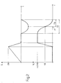
Figure 2 shows time graphs of the current flow in, and the voltage at the terminals of, the control transistor forming part of theFigure 1 dc-to-dc converter; -
Figure 3 shows a circuit diagram of a flyback resonant-transition dc-to-dc converter in accordance with a second embodiment of the present invention. - The present invention is based on the principle of only switching the control transistor from the cutoff to the saturation condition when the Snubber capacitor is discharged naturally and the voltage at its terminals is therefore substantially zero.
- To do this, according to a first embodiment of the present invention, the voltage at the terminals of the Snubber capacitor is measured directly, and the control transistor is only switched from the cutoff to the saturation condition when the measured voltage is less than or equal to a predetermined threshold value close to zero.
-
Number 1 inFigure 1 indicates as a whole a flyback resonant-transition dc-to-dc converter in accordance with a first embodiment of the present invention. -
Converter 1 comprises a first and asecond input terminal 2, 4 connected respectively, in use, to the positive and negative poles of an electrical energy source 6, e.g. a battery, supplying a supply voltage VB; and a number of pairs of output terminals (only two shown inFigure 1 ), each comprising a first and asecond output terminal Figure 1 by aresistor 12. -
Converter 1 comprises a stabilizingcapacitor 20 connected between first andsecond input terminals 2, 4; atransformer 22 comprising aprimary winding 24 interposed between first andsecond input terminals 2, 4, and a number ofsecondary windings 26, each connected to a respective pair ofoutput terminals diode 14 and acapacitor 16, as described later on; a bipolar or MOSFET control transistor 28 - bipolar in the example shown - in series withprimary winding 24; a Snubbercapacitor 30 in parallel withcontrol transistor 28; afirst comparator circuit 32 in parallel with Snubbercapacitor 30; asecond comparator circuit 34 in series withcontrol transistor 28; and acontrol circuit 36 for controllingcontrol transistor 28. - More specifically,
primary winding 24 has a first terminal connected to first input terminal 2 ofconverter 1; and a second terminal connected to the collector terminal ofcontrol transistor 28, which has the emitter terminal connected tosecond input terminal 4 ofconverter 1 viasecond comparator circuit 34, and the base terminal receiving a logic control signal T, which, at a high logic value, turns on control transistor 28 (which can be likened to a closed switch), and, at a low logic value, turns off control transistor 28 (which can be likened to an open switch). - Each
secondary winding 26 has a first terminal connected to the respectivefirst output terminal 8 ofconverter 1 viarespective diode 14; and a second terminal connected directly to the respectivesecond output terminal 10. Eachdiode 14 has an anode terminal connected to the first terminal ofsecondary winding 26, and a cathode terminal connected tooutput terminal 8; and eachcapacitor 16 is connected betweenrespective output terminals - The
first comparator circuit 32 has a first and second input terminal connected to the terminals of Snubbercapacitor 30; and an output terminal supplying a logic voltage level signal VS1, which assumes a high logic level when the voltage at the terminals ofSnubber capacitor 30 is less than or equal to a first predetermined threshold value VTH1, and a low logic level when the voltage at the terminals of Snubbercapacitor 30 is greater than first threshold value VTH1. - The first threshold value VTH1 conveniently ranges between zero and ten percent of the supply voltage VB supplied by electrical energy source 6. Obviously, the closer the first threshold value VTH1 is to zero, the lower the switching losses will be.
- The
second comparator circuit 34 has a first input terminal connected to the emitter terminal ofcontrol transistor 28; a second input terminal connected to thesecond input terminal 4 ofconverter 1; and an output terminal supplying a logic current level signal IS, which assumes a high logic level when the current flow incontrol transistor 28, and hence inprimary winding 24, is greater than or equal to a second predetermined threshold value ITH, and a low logic level when the current is less than the second threshold value ITH. - The second threshold value ITH depends on the power requested of
converter 1 and, in particular, increases alongside an increase in the difference between the desired output voltage and the actual output voltage. As such, when the output voltage of the converter tends to fall, due an increase in load, the second threshold value ITH increases in an attempt to compensate for the fall in output voltage. -
Control circuit 36 has a first and second input terminal connected respectively to, and receiving voltage level signal VS1 and current level signal IS from, the output terminals of first andsecond comparator circuits control transistor 28. - More specifically, control signal T switches from a low to a high logic state, corresponding to turn-on of
control transistor 28, when voltage level signal VS1 switches from a low to a high logic level, i.e. when the voltage at the terminals ofSnubber capacitor 30 is less than or equal to first threshold value VTH1; and switches from a high to a low logic state, corresponding to turn-off ofcontrol transistor 28, when current level signal IS switches from a low to a high logic level, i.e. when the current flow inprimary winding 24 oftransformer 22 is greater than or equal to second threshold value ITH. - Operation of
converter 1 will now be described with reference toFigure 2 , which shows time graphs of the current flow IL inprimary winding 24 oftransformer 22, and the voltage VC at the terminals ofSnubber capacitor 30. - An initial condition is assumed, in which
control transistor 28 is cut off,Snubber capacitor 30 is discharged, and voltage VC and current IL are both zero. - In this condition, the voltage level signal VS1 generated by
first comparator circuit 32 switches from a low to a high logic level, so that control signal T generated bycontrol circuit 36 also switches from a low to a high logic level, thus turning oncontrol transistor 28. - A closed loop is thus formed comprising electrical energy source 6,
primary winding 24 oftransformer 22,control transistor 28 andsecond comparator circuit 34, and a current IL increasing linearly in time flows inprimary winding 24 oftransformer 22 to store energy in the core oftransformer 22, while the voltage VC at the terminals of Snubbercapacitor 30 remains substantially nil. - When the current IL flowing in
primary winding 24 oftransformer 22 reaches first threshold value ITH, the current level signal IS generated bysecond comparator circuit 34 switches from a low to a high logic level, so that the control signal T generated bycontrol circuit 36 switches from a high to a low logic level, thus turning offcontrol transistor 28. - A closed loop is thus formed comprising electrical energy source 6,
primary winding 24 oftransformer 22,Snubber capacitor 30 andsecond comparator circuit 34, and the dc-to-dc converter operates in the following three steps: - A first step, in which the current IL flowing in
primary winding 24 decreases in time from value ITH to a value of substantially zero faster than the increase in current during the time interval in whichcontrol transistor 28 is closed. At this step, part of the energy stored in the core oftransformer 22 is therefore transferred, minus losses, to Snubbercapacitor 30, the voltage VC at the terminals of which increases from zero to a value equal to about twice the supply voltage VB supplied by the electrical energy source (in particular, equal to the supply voltage VB supplied by electrical energy source 6, plus the voltage "reflected" bysecondary windings 26 ontoprimary winding 24 of transformer 22). Since, at this step, the voltage at the terminals ofcontrol transistor 28 increases over a relatively long period of time, the switching losses caused bycontrol transistor 28 being turned off are extremely small. - A second step, in which the current IL flowing in
primary winding 24 remains substantially nil, the voltage at the terminals of Snubbercapacitor 30 remains substantially at a value equal to about twice the supply voltage VB supplied by electrical energy source 6, and a current induced by the magnetic energy stored in the core oftransformer 22 flows insecondary windings 26. - A third step, in which resonance occurs between primary winding 24 and Snubber
capacitor 30, so that a so-called resonant discharge occurs of the energy stored in Snubbercapacitor 30. During this step, the current IL flowing inprimary winding 24 assumes negative values and is substantially sinusoidal with a portion decreasing towards increasingly negative values (in absolute value) followed by a portion increasing once more towards zero values, while the voltage VC at the terminals of Snubbercapacitor 30 decreases substantially sinusoidally to a substantially zero value. - During the resonant discharge step - which lasts about half the resonance period of the circuit formed by primary winding 24 and by Snubber capacitor 30 - when the voltage VC at the terminals of
Snubber capacitor 30 reaches first threshold value VTH1, the control signal T generated bycontrol circuit 36 switches from a low to a high logic state, thus turningcontrol transistor 28 back on. -
Control transistor 28 switches from off to on at substantially zero voltage, so that the switching losses are extremely small. - Unlike known systems, therefore, in which Snubber
capacitor 30 is discharged beforecontrol transistor 28 switches from off to on, switching according to the present invention is effected when Snubbercapacitor 30 is naturally discharged. -
Figure 3 shows a flyback resonant-transition dc-to-dc converter in accordance with a second embodiment of the present invention, which is similar to dc-to-dc converter 1 and therefore only described below insofar as it differs from dc-to-dc converter 1, and using the same reference numbers for any parts identical with or corresponding to those already described. - The second embodiment of the present invention is based on the principle of detecting the instant in which the voltage at the terminals of
Snubber capacitor 30 is zeroed, by measuring an electric quantity correlated to the voltage at the terminals ofSnubber capacitor 30, as opposed to measuring the voltage itself. - More specifically, as shown in
Figure 2 , during the resonant discharge step, the current IL flowing in primary winding 24 oftransformer 22 assumes a maximum negative value - i.e. the voltage in primary winding 24, and therefore in secondary winding 26, is nil - when the voltage at the terminals ofSnubber capacitor 30 assumes a value equal to the voltage VB supplied by electrical energy source 6. This instant in time is indicated inFigure 2 by the letter P. - As the duration TA of the resonant discharge step is known, from LC resonator theory, to equal half the resonance period, i.e.

where L is the inductance of primary winding 24 oftransformer 22, and C the capacitance ofSnubber capacitor 30, the time TB between the instant the voltage VC at the terminals ofSnubber capacitor 30 equals the supply voltage VB supplied by electrical energy source 6, and the instant in which the voltage VC at the terminals ofSnubber capacitor 30 is zeroed, equals half duration TA, i.e.
Therefore, the instant the current IL flowing in primary winding 24 oftransformer 22 reaches the maximum negative value - i.e. the voltage at the terminals of secondary winding 26 is substantially zero - the voltage at the terminals ofSnubber capacitor 30 equals VB, so that, after a time equal to TB, the voltage at the terminals ofSnubber capacitor 30 is definitely zero, andcontrol transistor 28 can be turned on. -
Figure 3 shows a circuit diagram of a flyback resonant-transition dc-to-dc converter in accordance with a second embodiment of the present invention. - The
Figure 3 dc-to-dc converter, indicated as a whole by 1', differs from dc-to-dc converter 1 by the first comparator circuit, indicated 32', being connected in parallel with one ofsecondary windings 26, as opposed toSnubber capacitor 30, to detect the voltage between the terminals of secondary winding 26, which voltage is correlated, via the transformation ratio oftransformer 22, to the voltage in primary winding 24 oftransformer 22. - More specifically, first comparator circuit 32' is connected directly to the terminals of secondary winding 26 upstream from
diode 14, and generates at the output terminal a logic voltage level signal VS2, which assumes a high logic level when the voltage VA in secondary winding 26 is less than or equal to a third predetermined threshold value VTH2, and a low logic level when the voltage VA in secondary winding 26 is greater than third threshold value VTH2. - Third threshold value VTH2 conveniently ranges between zero and ten percent of the supply voltage VB supplied by electrical energy source 6 and referred back to secondary winding 26, taking into account the transformation ratio of
transformer 22. - Dc-to-dc converter 1' also comprises a
delay circuit 38 interposed between first comparator circuit 32' andcontrol circuit 36 to generate a delayed level signal VSR obtained by so delaying second voltage level signal VS2 that the switching edge from the low to high logic level of the delayed voltage level signal VSR occurs when the voltage at the terminals ofSnubber capacitor 30 is less than or equal to first threshold value VTH1. - More specifically, when second threshold value VTH2 assumes a zero value, the delay introduced by
delay circuit 38 equals the aforementioned time TB, whereas, for other values of second threshold value VTH2, the delay introduced bydelay circuit 38 is correlated to the value assumed by second threshold value VTH2, and, since the current flow pattern in primary winding 24 oftransformer 22 is known, can be calculated easily. - Converter 1' operates in the same way as dc-to-
dc converter 1 already described. - The advantages of
converters 1, 1' according to the present invention will be clear from the foregoing description. - As compared with known flyback resonant-transition converters employing the Snubber technique to reduce switching losses, the circuit structure of
converters 1, 1' is much simpler by requiring only two additional comparator circuits having a substantially negligible effect on the final cost of the converters. - Clearly, changes may be made to the dc-to-dc converters as described and illustrated herein without, however, departing from the scope of the present invention.
- For example, one of
secondary windings 26 of converter 1' in the second embodiment need not be connected to a respective pair ofoutput terminals - Moreover, the instant in which the current flowing in primary winding 24 of
transformer 22 is greater than or equal to the third threshold value may be detected otherwise than as described, and in particular also by detecting a voltage.
Claims (11)
- A resonant-transition, DC-DC converter (1) comprising first and second input terminals (2, 4) intended to be connected, in use, to an electrical energy source (6); at least first and second output terminals (8, 10) intended to be connected, in use, to a load (12); a transformer (22) comprising a primary winding (24) connected between said first and second input terminals (2, 4), and at least one secondary winding (26) connected between said first and second output terminals (8, 10); a controlled switch (28) connected between said primary winding (24) and one of said first and second input terminals (2, 4) and having a control terminal configured to receive a logic control signal (T) having a first switching edge for closing said controlled switch (28) and a second switching edge for opening said controlled switch (28); capacitive means (30) connected in parallel to said controlled switch (28); voltage level indicating means (32; 32', 38) configured to sense an electric quantity related to a voltage (VC) across said capacitive means (30) and generate a first logic voltage level signal (VS1; VSR) having a switching edge when said voltage (VC) across said capacitive means (30) is lower than or equal to a threshold voltage (VTH1; VTH2); and control means (36) configured to receive said first voltage level signal (VS1; VSR) and generate said control signal (T) for said controlled switching means (28) and with said first switching edge generated in response to said switching edge of said first voltage level signal (VS1; VSR); characterized in that said resonant-transition, DC-DC converted (1) further includes current level indicating means (34) configured to sense an electric quantity related to a current flowing in said primary winding (24) of said transformer (22) and generate a logic current level signal (IS) having a switching edge when said current is higher than or equal to a threshold current (ITH); and in that said control means (36) are further configured to receive also said current level signal (IS) and generate said control signal (T) for said controlled switch (28) and with said second switching edge generated in response to said switching edge of said current level signal (IS).
- The resonant-transition DC-DC converter of Claim 1, wherein said threshold voltage (VTH1; VTH2) conveniently ranges between zero and ten percent of a quantity related to a supply voltage (VB) of said electric energy source (6).
- The resonant-transition DC-DC converter of Claim 1 or 2, wherein said threshold current (ITH) is a function of the power requested to said converter (1).
- The resonant-transition DC-DC converter of any one of the foregoing Claims, wherein said threshold current (ITH) increases alongside an increase in the difference between a desired output voltage and an actual output voltage of said converter (1).
- The resonant-transition DC-DC converter of any one of the foregoing Claims, wherein said current level indicating means comprise a current comparator (34) series connected to said primary winding (24) of said transformer (22).
- The resonant-transition, DC-DC converter of Claim 1, wherein said voltage level indicating means comprise a voltage comparator (32) parallel connected to said capacitive means (30).
- The resonant-transition DC-DC converter of any one of the foregoing Claims 1 to 5, wherein said voltage level indicating means comprise a voltage comparator (32') configured to sense an electric quantity related to a voltage (VA) across said secondary winding (26) of said transformer (22), and generate a second logic voltage level signal (VS2) having a switching edge when said voltage (VA) across said secondary winding (26) is lower than or equal to said threshold voltage (VTH2); and delay means (38) cascade connected to said voltage comparator (32') to generate said first voltage level signal (VSR) by delaying said second voltage level signal (VS2) by a delay (TB) which is a function of said threshold voltage (VTH2).
- The resonant-transition DC-DC converter of Claim 7, wherein said voltage comparator (32') is parallel connected to said secondary winding (26) of said transformer (22).
- The resonant-transition DC-DC converter of Claim 7, wherein said transformer (22) comprises a further secondary winding (26), and said voltage comparator (32') is parallel connected to said further secondary winding (26).
- The resonant-transition DC-DC converter of any one of Claims 7 to 9, wherein said threshold voltage (VTH2) conveniently ranges between zero and ten percent of a quantity related to a supply voltage (VB) of said electric energy source (6) and to a transformation ratio of said transformer (22).
- The resonant-transition DC-DC converter of any one of Claims 7 to 10, wherein said threshold voltage (VTH2) is substantially zero, and said delay (TB) between said switching edge of said first voltage level signal (VSR) and said switching edge of said second voltage level signal (VS2) equals:

where TB is said delay, L is the inductance of said primary winding (24) of said transformer (22), and C is the capacitance of said capacitive means (30).
Applications Claiming Priority (3)
| Application Number | Priority Date | Filing Date | Title |
|---|---|---|---|
| ITTO990330 | 1999-04-23 | ||
| ITTP990330 | 1999-04-23 | ||
| IT1999TO000330A IT1308452B1 (en) | 1999-04-23 | 1999-04-23 | RESONANT TRANSITION DC-DC CONVERTER AND CONTROL METHOD OF RESONANT TRANSITION OF A DC-DC CONVERTER |
Publications (3)
| Publication Number | Publication Date |
|---|---|
| EP1047178A2 EP1047178A2 (en) | 2000-10-25 |
| EP1047178A3 EP1047178A3 (en) | 2001-06-20 |
| EP1047178B1 true EP1047178B1 (en) | 2011-01-05 |
Family
ID=11417752
Family Applications (1)
| Application Number | Title | Priority Date | Filing Date |
|---|---|---|---|
| EP00108751A Expired - Lifetime EP1047178B1 (en) | 1999-04-23 | 2000-04-25 | Resonant DC-to-DC converter and method of controlling the same |
Country Status (3)
| Country | Link |
|---|---|
| EP (1) | EP1047178B1 (en) |
| DE (1) | DE60045458D1 (en) |
| IT (1) | IT1308452B1 (en) |
Families Citing this family (1)
| Publication number | Priority date | Publication date | Assignee | Title |
|---|---|---|---|---|
| CA2789381C (en) | 2010-02-19 | 2015-10-20 | Queen's University At Kingston | A controller and a method of controlling a resonant power converter |
Family Cites Families (4)
| Publication number | Priority date | Publication date | Assignee | Title |
|---|---|---|---|---|
| JP3199423B2 (en) * | 1991-11-01 | 2001-08-20 | オリジン電気株式会社 | Resonant type forward converter |
| JP3116338B2 (en) * | 1994-03-22 | 2000-12-11 | 横河電機株式会社 | Switching power supply |
| DE69506096T2 (en) * | 1995-07-31 | 1999-04-15 | Hewlett-Packard Co., Palo Alto, Calif. | Flyback converter |
| US5680034A (en) * | 1995-09-22 | 1997-10-21 | Toko, Inc. | PWM controller for resonant converters |
-
1999
- 1999-04-23 IT IT1999TO000330A patent/IT1308452B1/en active
-
2000
- 2000-04-25 EP EP00108751A patent/EP1047178B1/en not_active Expired - Lifetime
- 2000-04-25 DE DE60045458T patent/DE60045458D1/en not_active Expired - Lifetime
Also Published As
| Publication number | Publication date |
|---|---|
| EP1047178A3 (en) | 2001-06-20 |
| ITTO990330A0 (en) | 1999-04-23 |
| ITTO990330A1 (en) | 2000-10-23 |
| DE60045458D1 (en) | 2011-02-17 |
| EP1047178A2 (en) | 2000-10-25 |
| IT1308452B1 (en) | 2001-12-17 |
Similar Documents
| Publication | Publication Date | Title |
|---|---|---|
| US6005782A (en) | Flyback converter with soft switching using auxiliary switch and resonant circuit | |
| JP2961897B2 (en) | Switching power supply | |
| US7773392B2 (en) | Isolated switching power supply apparatus | |
| US7023186B2 (en) | Two stage boost converter topology | |
| US6690143B2 (en) | Power factor correction circuit with resonant snubber | |
| US5847941A (en) | Switching power supply system and process | |
| US20060050537A1 (en) | Input stage circuit of three-level dc/dc converter | |
| WO2000048300A1 (en) | Offset resonance zero volt switching flyback converter | |
| KR100681689B1 (en) | Switching power supply | |
| US9912241B2 (en) | System and method for a cascode switch | |
| US10574148B1 (en) | Self-adjusting current injection technology | |
| JP3475892B2 (en) | Switching power supply | |
| Song et al. | Dual-bridge DC-DC converter: A new topology characterized with no deadtime operation | |
| US20060013020A1 (en) | Dc converter | |
| US20050180176A1 (en) | Welding set with quasi-resonant soft-switching inverter | |
| EP1771937A1 (en) | Automatic frequency control for series resonant switched mode power supply | |
| WO1998038727A2 (en) | Dc-dc converter with multiple outputs turned on and off in certain sequence | |
| EP1047178A2 (en) | Resonant DC-to-DC converter and method of controlling the same | |
| US5923155A (en) | Circuit for the production of an auxiliary voltage | |
| EP3739743A1 (en) | System and method for improving converter efficiency | |
| KR970003237B1 (en) | Soft switching circuit for separately-excited switching power source in current discontinuity mode | |
| EP1341144B1 (en) | Power circuit for a plasma display | |
| US20210242781A1 (en) | Power converter apparatus including llc resonant circuits and wide range of output voltage with higher efficiency | |
| RU2269858C1 (en) | Secondary power supply unit | |
| KR100591034B1 (en) | Half Bridge Power Converter |
Legal Events
| Date | Code | Title | Description |
|---|---|---|---|
| PUAI | Public reference made under article 153(3) epc to a published international application that has entered the european phase |
Free format text: ORIGINAL CODE: 0009012 |
|
| AK | Designated contracting states |
Kind code of ref document: A2 Designated state(s): DE ES FR GB IT SE |
|
| AX | Request for extension of the european patent |
Free format text: AL;LT;LV;MK;RO;SI |
|
| PUAL | Search report despatched |
Free format text: ORIGINAL CODE: 0009013 |
|
| AK | Designated contracting states |
Kind code of ref document: A3 Designated state(s): AT BE CH CY DE DK ES FI FR GB GR IE IT LI LU MC NL PT SE |
|
| AX | Request for extension of the european patent |
Free format text: AL;LT;LV;MK;RO;SI |
|
| 17P | Request for examination filed |
Effective date: 20011219 |
|
| AKX | Designation fees paid |
Free format text: DE ES FR GB IT SE |
|
| 17Q | First examination report despatched |
Effective date: 20090506 |
|
| GRAP | Despatch of communication of intention to grant a patent |
Free format text: ORIGINAL CODE: EPIDOSNIGR1 |
|
| GRAS | Grant fee paid |
Free format text: ORIGINAL CODE: EPIDOSNIGR3 |
|
| GRAA | (expected) grant |
Free format text: ORIGINAL CODE: 0009210 |
|
| AK | Designated contracting states |
Kind code of ref document: B1 Designated state(s): DE ES FR GB IT SE |
|
| REG | Reference to a national code |
Ref country code: GB Ref legal event code: FG4D |
|
| REF | Corresponds to: |
Ref document number: 60045458 Country of ref document: DE Date of ref document: 20110217 Kind code of ref document: P |
|
| REG | Reference to a national code |
Ref country code: DE Ref legal event code: R096 Ref document number: 60045458 Country of ref document: DE Effective date: 20110217 |
|
| PG25 | Lapsed in a contracting state [announced via postgrant information from national office to epo] |
Ref country code: ES Free format text: LAPSE BECAUSE OF FAILURE TO SUBMIT A TRANSLATION OF THE DESCRIPTION OR TO PAY THE FEE WITHIN THE PRESCRIBED TIME-LIMIT Effective date: 20110416 Ref country code: SE Free format text: LAPSE BECAUSE OF FAILURE TO SUBMIT A TRANSLATION OF THE DESCRIPTION OR TO PAY THE FEE WITHIN THE PRESCRIBED TIME-LIMIT Effective date: 20110105 |
|
| PLBE | No opposition filed within time limit |
Free format text: ORIGINAL CODE: 0009261 |
|
| STAA | Information on the status of an ep patent application or granted ep patent |
Free format text: STATUS: NO OPPOSITION FILED WITHIN TIME LIMIT |
|
| 26N | No opposition filed |
Effective date: 20111006 |
|
| GBPC | Gb: european patent ceased through non-payment of renewal fee |
Effective date: 20110425 |
|
| REG | Reference to a national code |
Ref country code: DE Ref legal event code: R097 Ref document number: 60045458 Country of ref document: DE Effective date: 20111006 |
|
| PG25 | Lapsed in a contracting state [announced via postgrant information from national office to epo] |
Ref country code: GB Free format text: LAPSE BECAUSE OF NON-PAYMENT OF DUE FEES Effective date: 20110425 |
|
| PGFP | Annual fee paid to national office [announced via postgrant information from national office to epo] |
Ref country code: DE Payment date: 20120502 Year of fee payment: 13 |
|
| PGFP | Annual fee paid to national office [announced via postgrant information from national office to epo] |
Ref country code: FR Payment date: 20120504 Year of fee payment: 13 |
|
| PGFP | Annual fee paid to national office [announced via postgrant information from national office to epo] |
Ref country code: IT Payment date: 20120418 Year of fee payment: 13 |
|
| PG25 | Lapsed in a contracting state [announced via postgrant information from national office to epo] |
Ref country code: DE Free format text: LAPSE BECAUSE OF NON-PAYMENT OF DUE FEES Effective date: 20131101 |
|
| REG | Reference to a national code |
Ref country code: FR Ref legal event code: ST Effective date: 20131231 |
|
| REG | Reference to a national code |
Ref country code: DE Ref legal event code: R119 Ref document number: 60045458 Country of ref document: DE Effective date: 20131101 |
|
| PG25 | Lapsed in a contracting state [announced via postgrant information from national office to epo] |
Ref country code: FR Free format text: LAPSE BECAUSE OF NON-PAYMENT OF DUE FEES Effective date: 20130430 Ref country code: IT Free format text: LAPSE BECAUSE OF NON-PAYMENT OF DUE FEES Effective date: 20130425 |