EP1047125A2 - Method for rapidly dechucking a semiconductor wafer from an electrostatic chuck utilizing a hysteretic discharge cycle - Google Patents
Method for rapidly dechucking a semiconductor wafer from an electrostatic chuck utilizing a hysteretic discharge cycle Download PDFInfo
- Publication number
- EP1047125A2 EP1047125A2 EP00303333A EP00303333A EP1047125A2 EP 1047125 A2 EP1047125 A2 EP 1047125A2 EP 00303333 A EP00303333 A EP 00303333A EP 00303333 A EP00303333 A EP 00303333A EP 1047125 A2 EP1047125 A2 EP 1047125A2
- Authority
- EP
- European Patent Office
- Prior art keywords
- dechucking
- voltage
- electrostatic chuck
- wafer
- workpiece
- Prior art date
- Legal status (The legal status is an assumption and is not a legal conclusion. Google has not performed a legal analysis and makes no representation as to the accuracy of the status listed.)
- Granted
Links
Images


Classifications
-
- H—ELECTRICITY
- H10—SEMICONDUCTOR DEVICES; ELECTRIC SOLID-STATE DEVICES NOT OTHERWISE PROVIDED FOR
- H10P—GENERIC PROCESSES OR APPARATUS FOR THE MANUFACTURE OR TREATMENT OF DEVICES COVERED BY CLASS H10
- H10P72/00—Handling or holding of wafers, substrates or devices during manufacture or treatment thereof
- H10P72/70—Handling or holding of wafers, substrates or devices during manufacture or treatment thereof for supporting or gripping
- H10P72/72—Handling or holding of wafers, substrates or devices during manufacture or treatment thereof for supporting or gripping using electrostatic chucks
- H10P72/722—Details of electrostatic chucks
-
- Y—GENERAL TAGGING OF NEW TECHNOLOGICAL DEVELOPMENTS; GENERAL TAGGING OF CROSS-SECTIONAL TECHNOLOGIES SPANNING OVER SEVERAL SECTIONS OF THE IPC; TECHNICAL SUBJECTS COVERED BY FORMER USPC CROSS-REFERENCE ART COLLECTIONS [XRACs] AND DIGESTS
- Y10—TECHNICAL SUBJECTS COVERED BY FORMER USPC
- Y10T—TECHNICAL SUBJECTS COVERED BY FORMER US CLASSIFICATION
- Y10T279/00—Chucks or sockets
- Y10T279/23—Chucks or sockets with magnetic or electrostatic means
Definitions
- the invention relates to a method of rapidly dechucking a semiconductor wafer from an electrostatic chuck. More particularly, the invention relates to a method of dechucking a wafer from an electrostatic chuck by using a hysteretic discharging cycle.
- Electrostatic chucks are used for holding a workpiece in various applications ranging from holding a sheet of paper in a computer graphics plotter to holding a semiconductor wafer within a semiconductor fabrication process chamber.
- electrostatic chucks vary in design, they all are based on the principle of applying a voltage to one or more electrodes in the chuck so as to induce opposite polarity charges in the workpiece and electrode(s), respectively. The electrostatic attractive force between the opposite charges presses the workpiece against the chuck, thereby retaining the workpiece.
- One problem that arises with the use of an ESC is the difficulty of removing the residual electrostatic force between the workpiece and the chuck during "dechucking". This residual force results from electric charges having accumulated at the interface between the workpiece and the ESC support surface.
- One technique for dechucking involves connecting both the electrode and the workpiece to ground. Another technique reverses the polarity of the DC chucking voltage applied to the electrodes to discharge the electrodes.
- these techniques are not completely effective at removing all the charge on the electrodes and the wafer. Consequently, a mechanical force is often needed to overcome the remaining attractive electrostatic force due to residual charges on the electrodes and wafer.
- a successful dechucking operation is one which leaves the wafer in a state subject to acceptably low residual electrostatic attractive force without "popping" the wafer.
- the time required to dechuck by these methods is defined by the RC time constant of the high voltage electrical circuit as well as the effective charge relaxation time constant of the electrode-wafer system.
- This time constant is given by the effective resistivity-permitivity product, where ⁇ is the volume resistivity of the dielectric layer between the electrode and the wafer (i.e., the chuck material), ⁇ 0 is the permittivity of free space, and is the relative permittivity of the dielectric layer.
- the total time required to dechuck by this method is often on the order of several seconds.
- dechucking methods include applying to the ESC an optimal, but non-zero, dechucking voltage.
- Another method involves determining and applying an optimal dechucking voltage for an optimal dechucking period.
- This is the subject of another commonly-assigned U.S. patent application Serial No. 08/696,293, filed by Loo on August 13, 1998, and is herein incorporated by reference.
- the wafer is dechucked by applying a DC voltage having a polarity opposite that of the chucking voltage, then applying a switched DC waveform (in effect, an AC waveform) to remove any residual charge.
- a DC voltage having a polarity opposite that of the chucking voltage
- a switched DC waveform in effect, an AC waveform
- the dechucking duration is exacerbated in systems where the platen supporting the wafer is vertically oriented during wafer processing, e.g., ion implant equipment.
- gravity does not aid the chucking process and, to ensure sufficient wafer retention white moving the platen to a vertical orientation, a very strong chucking force is required.
- Such a strong chucking force requires a substantial chucking voltage to be applied to the electrostatic chuck, i.e., typically much larger than the chucking voltage used in horizontally oriented chucks.
- This high chucking voltage causes a substantial residual charge to reside between the wafer and the chuck after the chucking voltage is deactivated.
- the use of conventional dechucking techniques does not remove this large residual charge in a short period of time. As such, the throughput of the wafer processing system is detrimentally impacted.
- the disadvantages of the prior art are overcome by a method and apparatus for dechucking a workpiece from an electrostatic chuck using a hysteretic dechucking cycle.
- the hysteretic cycle is derived from the well known hysteretic cycle used in magnetic degaussing signals to demagnetize objects such as cathode ray tubes (CRTS). It has been discovered that using a hysteretic cycle for an electric field that is applied to the interface of a workpiece and an electrostatic chuck workpiece support surface will effectively discharge the residual charge to zero or some predefined value.
- the inventive method is used to discharge a monopolar electrostatic chuck having a single electrode embedded in a dielectric chuck body.
- a wafer is positioned upon the chuck and in contact with a conductive contact.
- the contact applies a first voltage to the wafer.
- a second voltage having a magnitude different from the first voltage, is applied to the electrode within the chuck.
- the differential voltage from the wafer to the electrode causes charges to accumulate on the wafer and the electrode such that the wafer is retained upon chuck.
- the chuck body is fabricated of a semiconductive material such as aluminum nitride, the charges on the electrode migrate to the surface of the chuck body beneath the wafer.
- the surface charges on the chuck surface and the charges on the backside of the wafer retain the wafer on the chuck.
- This charge migration effect is known as the Johnsen-Rahbek effect.
- the Johnsen-Rahbek effect in a monopolar chuck provides a very effective and strong electrostatic force that retains the wafer.
- charge removal is also very difficult for such a chuck.
- the invention applies a voltage between the wafer and the electrode that performs a hysteretic discharge cycle such that residual charge is removed, i.e., a hysteretic electric field is established at the interface between the wafer support surface of the chuck and the wafer.
- the voltage used to produce such an electric field is a linearly decaying AC waveform.
- the form of this electric field at this interface is very important to achieving rapid dechucking of less than 200 mS.
- a proper discharging field is also achieved using a AC waveform having a linearly increasing frequency (i.e., the waveform is chirped).
- the end result of the hysteretic cycle used for discharging an electrostatic chuck is that the chuck even a monopolar chuck can be discharged very rapidly, i.e., in less than 200 mS. Consequently, a single wafer semiconductor processing system, such as a single wafer ion implant system, can process wafers with a very high throughput.
- Fig. 1 is a schematic illustration of a cross-sectional view of a semiconductor wafer processing system 100, for example, an ion implant system containing a monopolar electrostatic chuck (ESC) for retaining a wafer 114 within the system during wafer processing.
- the ion implant system 100 comprises a vacuum chamber 100, an ion beam source 104, an electrostatic chuck 106, a high voltage power supply 110 and an ESC controller 112.
- the ESC 106 contains an electrode 108 embedded in a dielectric chuck body 116.
- the dielectric chuck body 116 is fabricated of cylindrical puck of ceramic material such as aluminum nitride.
- dielectric materials can also be used, but aluminum nitride as well as boron-nitride, alumina doped with a titanium oxide or a chromium oxide promote the Johnsen-Rahbek effect (as described more fully below).
- the electrode 108 is a plate or layer of a conductive material such as molybdenum.
- the electrode 108 is connected to one terminal of the high voltage power supply 110.
- the other terminal of the supply 110 is connected through the chuck body to a surface electrode or pin 118 extending from the wafer support surface 120.
- the pin 118 is designed to contact the backside of the wafer such that the chucking voltage, e.g., 500 VDC, is applied by the supply 110 to the electrode 108 on the wafer 114.
- J-R monopolar chuck is described as one illustrative type of electrostatic chuck that can be used with the invention, any electrostatic chuck that requires rapid discharge of a residual charge will find the present invention useful.
- Such chucks include bipolar chucks, dielectric chucks, multi-electrode chucks, non-Johnsen-Rahbek chucks, and the like.
- the present invention is a method of rapid dechucking of the semiconductor wafer 114 by applying a hysteretic discharge cycle to the ESC 106.
- rapid dechucking time for a ceramic ESC used in an ion implant system is on the order of less than 200msec.
- This hysteretic behavior can be illustrated by a field-charge hysteresis curve 200, which is shown in Fig. 2a, where the residual charge 202 on an ESC is plotted as a function of the applied electric field 204.
- the charge on the ESC follows the path AB when an increasing voltage of positive polarity is applied to the electrode-wafer.
- the ESC charge follows the path BC, instead of BA, because of hysteresis.
- Applying a similar voltage cycle at a reversed polarity brings the ESC charge along The paths CD and DA, thus completing a full hysteretic cycle.
- the shape of this hysteresis curve is also rime dependent, because the residual charge on the ESC will, after the applied voltage is removed from the electrode, dissipate over time due to natural charge leakage.
- Equation (1) This charge leakage, or relaxation term is given by in Equation (1), which shows that as time approaches infinity, the surface charge becomes zero.
- This time-dependency of the hysteresis curve can therefore be represented in a three-dimensional plot, with the time axis being orthogonal to the charge and field axes 202 and 204 shown in Fig. 2a.
- degaussing which involves applying an external field to drive a magnet through its magnetization curve similar to that shown in Fig. 2a, has been used successfully for demagnetizing a magnet.
- a similar technique can also be used to return any "electret" to a zero charge state from any initial charge state.
- An electret is the electrostatic analogue of the magnet. Drawing from this analogy, a ferrous material can be made into a permanent magnet by subjecting the material to a magnetic field. Once removed from this field, the material retains a magnetic moment. Similarly, a dielectric material can be subject to an electrostatic field and made to retain charge once removed from this field.
- the electret effect can be exacerbated by application of a strong electric field, suitable choice of a susceptible material and by increasing molecular mobility, usually by subjecting the material to elevated temperature or increasing exposure time.
- a hot process with an ESC provides fertile pound for the formation of an electret.
- a decaying, periodic signal is used to cyclicly and gradually reduce the field seen by the electret (the wafer-ESC interface).
- the technique works because of the time and field dependence of the hysteresis. However, its effectiveness is determined by the amplitude decrement and frequency.
- this hysteretic behavior can advantageously be applied to the dechucking operation of an ESC, by subjecting the ESC to an alternating field whose magnitude, or peak amplitude, decreases over time. If the ESC is driven through a discharge voltage period having a peak amplitude (i.e., values of the field at B and D) which decreases with time, one can see the ESC hysteretic loop will become increasingly smaller upon successive cycles.
- the complete discharge cycle ends when the applied peak voltage approaches zero, and the ESC is left at a zero residual charge state (or some predefined level).
- the hysteretic response for the ESC during such a dechucking operation is illustrated in Fig. 2b, where the ESC charge follows the path ABCD-EFGH, and so on, until it reaches the zero charge state at the end of the discharge voltage cycle.
- the discharge waveform is oscillatory (sinusoidal) with a peak amplitude that decreases with time.
- Figs. 3a and 3b illustrate two possible signal profiles.
- Fig. 3a is a discharging signal waveform with a periodic sinusoidal oscillation whose peak amplitude decreases logarithmically as a function of time. That is, the peak amplitude in Fig.
- V c is the first peak value (generally the same or slightly larger than the magnitude of the chucking voltage)
- f is the frequency of the sinusoidal signal
- ⁇ is the "1/e" time associated with the exponential decay envelope (shown as dashed line)
- V x is the final voltage value after discharge is complete.
- the value of V x may be zero or non-zero
- this peak amplitude further decreases for each successive half-time period according to an exponential function, until it becomes V x after many time periods.
- the residual charge is reduced to a non-zero, nominal level that permits wafer removal.
- the overall dechucking time is shortened.
- a residual non-zero force may be useful in applications where the workpiece may slide off the chuck surface unless some force retains the workpiece until a workpiece manipulator can retrieve the workpiece from the chuck.
- a residual charge may be desirable to repel charged particles from the chuck surface after the wafer is removed from the chuck.
- the present invention generally provides a discharge cycle having a signal waveform such that this zero charge state (or nominal charge state) can be achieved for the electrostatic chuck system within a predetermined, or desired, dechucking time t d .
- the desired dechucking time may vary depending on the specific process application. In general, a shorter dechucking time is desirable because it translates directly to an increased process throughput.
- Fig. 3b Another signal profile suitable for use as a dechucking voltage is illustrated in Fig. 3b. Similar to the case in Fig. 3a, the signal is periodic in nature, except that the peak amplitude in Fig. 3b decreases linearly as a function of time. That is, - , where t 0 is a time in which the envelope is designed to reach V x as illustrated by the dashed line, and f is the frequency of oscillation.
- both of these profiles shown in Figs. 3a and 3b are open loop in the control sense, i.e., the signal is applied to the electrode without any control feedback as to the charge condition of the chuck, the discharging method is stable and convergent if the following two conditions are satisfied: 1) the initial field magnitude is greater than or equal to the greatest field experienced by the electret prior to the dechucking step; and 2) the frequency of oscillation is sufficiently low. This result occurs because all state trajectories are asymptotically captured in the diminishing magnitude envelope. In terms of nonlinear dynamics, all possible state trajectories are "attracted" to this particular state trajectory.
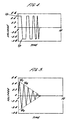
- Fig. 4 Another alternative discharging waveform is shown in Fig. 4. Unlike the profiles shown in Figs. 3a and 3b, this particular signal profile has a peak amplitude which remains constant over time. It also incorporates an increasing frequency "chirp', i.e., a positive frequency change which increases with time. For example, the frequency may vary from 100 Hz to 100 KHz. Since the ESC system inherently incorporates multiple first order lags, the voltage experienced by the ESC surface is actually an attenuated version of the power supply (applied) signal.
- chirp' i.e., a positive frequency change which increases with time.
- the frequency may vary from 100 Hz to 100 KHz. Since the ESC system inherently incorporates multiple first order lags, the voltage experienced by the ESC surface is actually an attenuated version of the power supply (applied) signal.
- this attenuation increases with increasing frequency, and an applied signal having a constant peak amplitude, but variable frequency "chirp", will produce an effective oscillating signal with a decaying peak amplitude at the interface of the ESC and the wafer. Therefore, this particular embodiment illustrates that the applied field is only of "secondary" importance when compared to the field actually experienced at the interface of the chuck surface and the wafer.
- the effective peak voltage at the ESC-wafer interface is caused to oscillate and decrease with time, a dechucking operation using the present invention can result in a zero charge state (or a predefined charge stale) at the end of the dechucking voltage cycle, even if the applied voltage as maintained at a constant peak amplitude.
- a decaying sinusoid signal for discharging the ESC is subject to certain frequency limitations due to the inherent first order lag between the surface charge accumulation and the charge accumulation at the electrodes. For example, it has been found experimentally that too fast a discharging frequency will result in some residual surface charge.
- an aluminum nitride (Johnsen-Rahbek) ESC was charged to 200 volts.
- the ESC electrodes were disconnected from the power supply and simultaneously shunted to an RL network, resulting in an exponentially decaying sinusoidal oscillation in electrode potential.
- the frequency of oscillation was between 100 and 200 kHz.
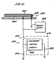
- FIG. 6 depicts a schematic of a passive dechucking circuit 600 coupled to an electrostatic chuck 602.
- the electrode 604 or electrode(s) of the electrostatic chuck 602 are driven by a power supply 606.
- the electrode 604 is connected to one polarity of a DC power supply 606 and the other polarity (ground) is connected to a contact 608 that conductively contacts the wafer 610 in one or more locations on the backside of the wafer 610.
- the dechucking circuit 600 comprises a switch 612, an inductor 614 and a resistive load 616.
- the resistive load 616 contains a discharge control circuit 618 connected to a resistor 620.
- the discharge control circuit 618 may be an active or passive circuit that controls the amount of energy dissipated by the resistor 620 during each cycle of the oscillatory discharge signal.
- the oscillatory signal is passively generated, in that, the wafer-chuck interface forms a capacitor that discharges its stored energy through an inductive load thus producing a resonant circuit.
- the resistor 620 dissipates energy from the resonant circuit during each cycle of oscillation. As such, the resistor controls the decay profile of the oscillating waveform that produces the electric field having a hysteretic cycle at the wafer-chuck interface.
- the resistive value can be dynamically adjusted by the discharge control circuit 618 to achieve an optimal profile for the decaying signal.
- the impedance may be linearly varying over time by using a positive temperature coefficient (PTC) resistor such that a different amount of energy is removed from the ESC-wafer interface with each cycle (i.e., the discharge control circuit and resistor would be a single device in a PTC resistor).
- PTC positive temperature coefficient
- a pair of oppositely polarized diodes connected in parallel are connected in series with the resistor 620.
- Another example would be to use an active control circuit such as a transistor circuit to control the dissipation during each cycle.
- discharge control circuits are merely examples of the myriad of possible circuits that those skilled in the art could derive to control the amount of energy dissipated by the resistive load and thus control the profile of the decaying signal. All such circuits should be considered within the scope of the invention.
Landscapes
- Container, Conveyance, Adherence, Positioning, Of Wafer (AREA)
- Jigs For Machine Tools (AREA)
Abstract
Description


Claims (20)
- A method of chucking and dechucking a workpiece from an electrostatic chuck comprising the step of:applying a chucking voltage to an electrode within said electrostatic chuck to electrostatically retain said workpiece upon a workpiece support surface of the electrostatic chuck;applying a dechucking voltage having an oscillating waveform to said electrode to produce an electric field having a hysteretic cycle between the workpiece and the workpiece support surface of the electrostatic chuck, whereby the electric field having a hysteretic cycle discharges charges that have accumulated between the workpiece and the workpiece support surface of the electrostatic chuck.
- The method of claim 1 wherein said electrostatic chuck is a monopolar electrostatic chuck having said chucking and dechucking voltages applied across the workpiece and an electrode within the electrostatic chuck.
- The method of claim 1 wherein the chucking voltage is a DC voltage.
- The method of claim 1 wherein said dechucking voltage has a peak amplitude which diminishes with time.
- The method of claim 1 wherein said dechucking voltage has a peak amplitude which linearly diminishes with time.
- The method of claim 1 wherein said dechucking voltage increase in frequency with time.
- The method of claim I wherein said dechucking voltage is passively produced using energy stored between the workpiece and electrostatic chuck.
- The method of claim 7 wherein the stored energy is discharged through a resistive and inductive loading circuit, where the resistance of a resistive element is defined to produce a specific discharge profile.
- The method of claim 7 further comprising the step of actively controlling the resistance of the resistive element during discharge.
- In an ion implant system having a monopolar electrostatic chuck, a method of chucking and dechucking a semiconductor wafer comprising the steps of:applying a chucking voltage to an electrode within said electrostatic chuck to electrostatically retain said semiconductor wafer upon a wafer support surface of the electrostatic chuck;processing said semiconductor wafer;applying a dechucking voltage having an oscillating waveform to said electrode to produce an electric field having a hysteretic cycle between the semiconductor wafer and the wafer support surface of the electrostatic chuck, whereby the electric field having a hysteretic cycle discharges charges that have accumulated between the semiconductor wafer and the wafer support surface of the electrostatic chuck.
- The method of claim 10 wherein the chucking voltage is a DC voltage.
- The method of claim 10 wherein said dechucking voltage has a peak amplitude which diminishes with time.
- The method of claim 10 wherein said dechucking voltage has a peak amplitude which linearly diminishes with time.
- The method of claim 10 wherein said dechucking voltage increase in frequency with time.
- The method of claim 10 wherein said dechucking voltage is passively produced using energy stored between the workpiece and electrostatic chuck.
- The method of claim 15 wherein the stored energy is discharged through a resistive and inductive loading circuit, where the resistance of a resistive element is defined to produce a specific discharge profile.
- The method of claim 15 further comprising the step of actively controlling the impedance of the resistive element during discharge.
- Apparatus for dechucking a workpiece from an electrostatic chuck having at least one electrode comprising:an inductor selectively coupled between said at least one etectrode and ground;a resistive element, selectively coupled between said at least one electrode and ground, having a resistance value that produces a specific discharge voltage profile for energy stored between said workpiece and a workpiece support surface of said electrostatic chuck.
- The apparatus of claim 18 wherein the resistive element is actively controlled to dissipate specified amounts of energy.
- The apparatus of claim 18 wherein said resistive element contains a passive control device and a resistive load device, wherein the passive control device controls an amount of energy to be dissipated by the resistive load device.
Applications Claiming Priority (2)
| Application Number | Priority Date | Filing Date | Title |
|---|---|---|---|
| US09/294,255 US6236555B1 (en) | 1999-04-19 | 1999-04-19 | Method for rapidly dechucking a semiconductor wafer from an electrostatic chuck utilizing a hysteretic discharge cycle |
| US294255 | 1999-04-19 |
Publications (3)
| Publication Number | Publication Date |
|---|---|
| EP1047125A2 true EP1047125A2 (en) | 2000-10-25 |
| EP1047125A3 EP1047125A3 (en) | 2004-01-21 |
| EP1047125B1 EP1047125B1 (en) | 2006-11-29 |
Family
ID=23132573
Family Applications (1)
| Application Number | Title | Priority Date | Filing Date |
|---|---|---|---|
| EP00303333A Expired - Lifetime EP1047125B1 (en) | 1999-04-19 | 2000-04-19 | Method for rapidly dechucking a semiconductor wafer from an electrostatic chuck utilizing a hysteretic discharge cycle |
Country Status (4)
| Country | Link |
|---|---|
| US (1) | US6236555B1 (en) |
| EP (1) | EP1047125B1 (en) |
| JP (1) | JP4610042B2 (en) |
| DE (1) | DE60032050T2 (en) |
Cited By (1)
| Publication number | Priority date | Publication date | Assignee | Title |
|---|---|---|---|---|
| WO2007136809A3 (en) * | 2006-05-18 | 2008-03-20 | Varian Semiconductor Equipment | Electrostatic chuck to limit particle deposits thereon |
Families Citing this family (39)
| Publication number | Priority date | Publication date | Assignee | Title |
|---|---|---|---|---|
| US6965506B2 (en) * | 1998-09-30 | 2005-11-15 | Lam Research Corporation | System and method for dechucking a workpiece from an electrostatic chuck |
| JP2003060018A (en) * | 2001-08-13 | 2003-02-28 | Nissin Electric Co Ltd | Substrate adsorption method and apparatus |
| JP4266586B2 (en) * | 2001-08-22 | 2009-05-20 | 株式会社村田製作所 | Post-test processing method for porcelain capacitors |
| US20040031699A1 (en) * | 2002-08-19 | 2004-02-19 | Applied Materials, Inc. | Method for performing real time arcing detection |
| DE10247051A1 (en) * | 2002-10-09 | 2004-04-22 | Polymer Latex Gmbh & Co Kg | Latex and process for its manufacture |
| SG125948A1 (en) * | 2003-03-31 | 2006-10-30 | Asml Netherlands Bv | Supporting structure for use in a lithographic apparatus |
| US7100954B2 (en) * | 2003-07-11 | 2006-09-05 | Nexx Systems, Inc. | Ultra-thin wafer handling system |
| US7072165B2 (en) * | 2003-08-18 | 2006-07-04 | Axcelis Technologies, Inc. | MEMS based multi-polar electrostatic chuck |
| US6947274B2 (en) * | 2003-09-08 | 2005-09-20 | Axcelis Technologies, Inc. | Clamping and de-clamping semiconductor wafers on an electrostatic chuck using wafer inertial confinement by applying a single-phase square wave AC clamping voltage |
| US7072166B2 (en) * | 2003-09-12 | 2006-07-04 | Axcelis Technologies, Inc. | Clamping and de-clamping semiconductor wafers on a J-R electrostatic chuck having a micromachined surface by using force delay in applying a single-phase square wave AC clamping voltage |
| US6946403B2 (en) * | 2003-10-28 | 2005-09-20 | Axcelis Technologies, Inc. | Method of making a MEMS electrostatic chuck |
| US7375946B2 (en) * | 2004-08-16 | 2008-05-20 | Applied Materials, Inc. | Method and apparatus for dechucking a substrate |
| US7244311B2 (en) * | 2004-10-13 | 2007-07-17 | Lam Research Corporation | Heat transfer system for improved semiconductor processing uniformity |
| CN101278385B (en) * | 2004-11-04 | 2011-10-12 | 株式会社爱发科 | Electrostatic chuck device |
| US7804675B2 (en) * | 2005-05-20 | 2010-09-28 | Tsukuba Seiko Ltd. | Electrostatic holding apparatus and electrostatic tweezers using the same |
| US20070195482A1 (en) * | 2006-02-23 | 2007-08-23 | Varian Semiconductor Equipment Associates, Inc. | Johnsen-Rahbek electrostatic chuck driven with AC voltage |
| KR101394337B1 (en) * | 2006-08-30 | 2014-05-13 | 엘아이지에이디피 주식회사 | Electrostratic Chuck |
| US7751172B2 (en) * | 2006-10-18 | 2010-07-06 | Axcelis Technologies, Inc. | Sliding wafer release gripper/wafer peeling gripper |
| KR101312292B1 (en) * | 2006-12-11 | 2013-09-27 | 엘아이지에이디피 주식회사 | Device of preventing substrate of plasma processing apparatus from breakdown and method of thereof |
| KR101295776B1 (en) * | 2007-08-02 | 2013-08-12 | 삼성전자주식회사 | Method of de-chucking a wafer using a direct voltage and a alternating voltage alternately and apparatus for fabricating a semiconductor device employing the same |
| US7813103B2 (en) * | 2007-10-11 | 2010-10-12 | Applied Materials, Inc. | Time-based wafer de-chucking from an electrostatic chuck having separate RF BIAS and DC chucking electrodes |
| US20090109595A1 (en) * | 2007-10-31 | 2009-04-30 | Sokudo Co., Ltd. | Method and system for performing electrostatic chuck clamping in track lithography tools |
| CN101872733B (en) * | 2009-04-24 | 2012-06-27 | 中微半导体设备(上海)有限公司 | Systems and methods for sensing and removing residual charge from processed semiconductor process pieces |
| JP5923245B2 (en) * | 2011-03-30 | 2016-05-24 | 東京エレクトロン株式会社 | Substrate removal method and storage medium |
| JP2013191802A (en) * | 2012-03-15 | 2013-09-26 | Fujitsu Semiconductor Ltd | Method for manufacturing semiconductor device |
| US8773817B2 (en) * | 2012-07-24 | 2014-07-08 | Lsi Corporation | Storage device having degauss circuitry with ramp generator for use in generating chirped degauss signal |
| DE102012109073A1 (en) * | 2012-09-26 | 2014-03-27 | Fraunhofer-Gesellschaft zur Förderung der angewandten Forschung e.V. | Method for operating a gripping device and electrostatic gripping device |
| US9101038B2 (en) * | 2013-12-20 | 2015-08-04 | Lam Research Corporation | Electrostatic chuck including declamping electrode and method of declamping |
| US10707110B2 (en) | 2015-11-23 | 2020-07-07 | Lam Research Corporation | Matched TCR joule heater designs for electrostatic chucks |
| JP6505027B2 (en) * | 2016-01-04 | 2019-04-24 | 株式会社日立ハイテクノロジーズ | Sample detachment method and plasma processing apparatus |
| US11387135B2 (en) | 2016-01-28 | 2022-07-12 | Applied Materials, Inc. | Conductive wafer lift pin o-ring gripper with resistor |
| JP6723660B2 (en) | 2017-03-24 | 2020-07-15 | 住友重機械イオンテクノロジー株式会社 | Wafer holding device and wafer attaching/detaching method |
| JP7340953B2 (en) * | 2019-04-26 | 2023-09-08 | 東京エレクトロン株式会社 | Static elimination method, substrate processing method, and substrate processing device |
| JP6935528B2 (en) * | 2020-03-02 | 2021-09-15 | 浜松ホトニクス株式会社 | Power supply for electrostatic chuck device, electrostatic chuck device, and dechuck control method |
| KR102677251B1 (en) * | 2021-10-28 | 2024-06-20 | 세메스 주식회사 | Substrate test apparatus and method for measuring dechucking force using the same |
| KR102728811B1 (en) * | 2021-11-23 | 2024-11-13 | 피에스케이 주식회사 | Support unit and substrate processing apparatus including same |
| CN114743901A (en) * | 2022-05-06 | 2022-07-12 | 北京北方华创微电子装备有限公司 | Semiconductor process chamber, wafer release method and semiconductor process equipment |
| FR3165547A1 (en) | 2024-08-09 | 2026-02-13 | C-Click | DEVICE AND METHOD FOR ELECTROSTATIC CLAMPING OF A SUPPORT PLATE CONTAINING A DIELECTRIC MATERIAL |
| WO2026033113A1 (en) | 2024-08-09 | 2026-02-12 | C-Click | Electrostatic wafer clamping device and method |
Family Cites Families (12)
| Publication number | Priority date | Publication date | Assignee | Title |
|---|---|---|---|---|
| JPS6244332A (en) * | 1985-08-23 | 1987-02-26 | Canon Inc | Electrostatic adsorption device |
| JPS63169244A (en) | 1987-01-06 | 1988-07-13 | Canon Inc | Sample holding device |
| US5103367A (en) * | 1987-05-06 | 1992-04-07 | Unisearch Limited | Electrostatic chuck using A.C. field excitation |
| JPH04246843A (en) * | 1991-01-31 | 1992-09-02 | Kyocera Corp | Controlling device for electrostatic chuck |
| US5315473A (en) * | 1992-01-21 | 1994-05-24 | Applied Materials, Inc. | Isolated electrostatic chuck and excitation method |
| FR2700219B1 (en) * | 1993-01-06 | 1995-02-17 | Saint Louis Inst | Method for electrically depolarizing a ferroelectric material and its application for obtaining ferroelectric material with reinforced rigidity. |
| US5444597A (en) * | 1993-01-15 | 1995-08-22 | Blake; Julian G. | Wafer release method and apparatus |
| JP3257180B2 (en) * | 1993-09-21 | 2002-02-18 | ソニー株式会社 | Film formation method |
| JP2976861B2 (en) * | 1994-09-30 | 1999-11-10 | 日本電気株式会社 | Electrostatic chuck and method of manufacturing the same |
| JPH08250579A (en) * | 1995-03-14 | 1996-09-27 | Mitsubishi Electric Corp | Power supply for electrostatic chuck of semiconductor manufacturing apparatus and semiconductor manufacturing apparatus |
| US5790365A (en) * | 1996-07-31 | 1998-08-04 | Applied Materials, Inc. | Method and apparatus for releasing a workpiece from and electrostatic chuck |
| JPH10284583A (en) * | 1997-04-04 | 1998-10-23 | Mitsubishi Electric Corp | Electrostatic chuck static elimination method and semiconductor manufacturing apparatus |
-
1999
- 1999-04-19 US US09/294,255 patent/US6236555B1/en not_active Expired - Lifetime
-
2000
- 2000-04-19 JP JP2000118199A patent/JP4610042B2/en not_active Expired - Lifetime
- 2000-04-19 DE DE60032050T patent/DE60032050T2/en not_active Expired - Fee Related
- 2000-04-19 EP EP00303333A patent/EP1047125B1/en not_active Expired - Lifetime
Cited By (2)
| Publication number | Priority date | Publication date | Assignee | Title |
|---|---|---|---|---|
| WO2007136809A3 (en) * | 2006-05-18 | 2008-03-20 | Varian Semiconductor Equipment | Electrostatic chuck to limit particle deposits thereon |
| US7583491B2 (en) | 2006-05-18 | 2009-09-01 | Varian Semiconductor Equipment Associates, Inc. | Electrostatic chuck to limit particle deposits thereon |
Also Published As
| Publication number | Publication date |
|---|---|
| JP4610042B2 (en) | 2011-01-12 |
| DE60032050D1 (en) | 2007-01-11 |
| DE60032050T2 (en) | 2007-04-05 |
| US6236555B1 (en) | 2001-05-22 |
| EP1047125A3 (en) | 2004-01-21 |
| EP1047125B1 (en) | 2006-11-29 |
| JP2001007191A (en) | 2001-01-12 |
Similar Documents
| Publication | Publication Date | Title |
|---|---|---|
| EP1047125B1 (en) | Method for rapidly dechucking a semiconductor wafer from an electrostatic chuck utilizing a hysteretic discharge cycle | |
| CN100459094C (en) | Adsorption and release of semiconductor wafers on J-R electrostatic chucks with micromachined surfaces by using force delay when a single-phase square-wave AC adsorption voltage is applied | |
| US6307728B1 (en) | Method and apparatus for dechucking a workpiece from an electrostatic chuck | |
| US5790365A (en) | Method and apparatus for releasing a workpiece from and electrostatic chuck | |
| US5818682A (en) | Method and apparatus for optimizing a dechucking period used to dechuck a workpiece from an electrostatic chuck | |
| WO2007100571A2 (en) | Johnsen-rahbek electrostatic chuck driven with ac voltage | |
| JPH0729968A (en) | Improved electrostatic chuck | |
| CN100459093C (en) | System and method for chucking semiconductor wafers on an electrostatic chuck | |
| EP1096561A2 (en) | Method for rapid dechucking of a semiconductor wafer from an electrostatic chuck | |
| US8228658B2 (en) | Variable frequency electrostatic clamping | |
| JP2017123354A (en) | Sample detachment method and plasma processing apparatus | |
| US6238160B1 (en) | Method for transporting and electrostatically chucking a semiconductor wafer or the like | |
| TWI307122B (en) | Method and apparatus for dynamic plasma treatment of bipolar esc system | |
| CN114743901A (en) | Semiconductor process chamber, wafer release method and semiconductor process equipment | |
| GB2293689A (en) | Electrostatic chuck | |
| JP2002222850A (en) | Detachment method of adsorbed object in electrostatic chuck | |
| WO2007136809A2 (en) | Electrostatic chuck to limit particle deposits thereon | |
| JPH0263304B2 (en) | ||
| JPH04246843A (en) | Controlling device for electrostatic chuck | |
| KR20030020072A (en) | Unipolar electro-static chuck | |
| JPH0786380A (en) | Electrostatic chuck | |
| JP2025137172A (en) | Power supply system and power supply method for electrostatic chuck | |
| JP2026043619A (en) | Method for detecting substrate adsorption state and substrate processing apparatus | |
| KR20050049725A (en) | Electro static chuck for preventing sticking |
Legal Events
| Date | Code | Title | Description |
|---|---|---|---|
| PUAI | Public reference made under article 153(3) epc to a published international application that has entered the european phase |
Free format text: ORIGINAL CODE: 0009012 |
|
| AK | Designated contracting states |
Kind code of ref document: A2 Designated state(s): AT BE CH CY DE DK ES FI FR GB GR IE IT LI LU MC NL PT SE |
|
| AX | Request for extension of the european patent |
Free format text: AL;LT;LV;MK;RO;SI |
|
| PUAL | Search report despatched |
Free format text: ORIGINAL CODE: 0009013 |
|
| AK | Designated contracting states |
Kind code of ref document: A3 Designated state(s): AT BE CH CY DE DK ES FI FR GB GR IE IT LI LU MC NL PT SE |
|
| AX | Request for extension of the european patent |
Extension state: AL LT LV MK RO SI |
|
| 17P | Request for examination filed |
Effective date: 20040706 |
|
| AKX | Designation fees paid |
Designated state(s): DE GB |
|
| GRAP | Despatch of communication of intention to grant a patent |
Free format text: ORIGINAL CODE: EPIDOSNIGR1 |
|
| GRAS | Grant fee paid |
Free format text: ORIGINAL CODE: EPIDOSNIGR3 |
|
| GRAA | (expected) grant |
Free format text: ORIGINAL CODE: 0009210 |
|
| AK | Designated contracting states |
Kind code of ref document: B1 Designated state(s): DE GB |
|
| REG | Reference to a national code |
Ref country code: GB Ref legal event code: FG4D |
|
| REF | Corresponds to: |
Ref document number: 60032050 Country of ref document: DE Date of ref document: 20070111 Kind code of ref document: P |
|
| PLBE | No opposition filed within time limit |
Free format text: ORIGINAL CODE: 0009261 |
|
| STAA | Information on the status of an ep patent application or granted ep patent |
Free format text: STATUS: NO OPPOSITION FILED WITHIN TIME LIMIT |
|
| 26N | No opposition filed |
Effective date: 20070830 |
|
| PGFP | Annual fee paid to national office [announced via postgrant information from national office to epo] |
Ref country code: GB Payment date: 20090312 Year of fee payment: 10 |
|
| PGFP | Annual fee paid to national office [announced via postgrant information from national office to epo] |
Ref country code: DE Payment date: 20090430 Year of fee payment: 10 |
|
| GBPC | Gb: european patent ceased through non-payment of renewal fee |
Effective date: 20100419 |
|
| PG25 | Lapsed in a contracting state [announced via postgrant information from national office to epo] |
Ref country code: DE Free format text: LAPSE BECAUSE OF NON-PAYMENT OF DUE FEES Effective date: 20101103 |
|
| PG25 | Lapsed in a contracting state [announced via postgrant information from national office to epo] |
Ref country code: GB Free format text: LAPSE BECAUSE OF NON-PAYMENT OF DUE FEES Effective date: 20100419 |