EP1046962A2 - Radio hologram observation apparatus and method therefor - Google Patents
Radio hologram observation apparatus and method therefor Download PDFInfo
- Publication number
- EP1046962A2 EP1046962A2 EP00108558A EP00108558A EP1046962A2 EP 1046962 A2 EP1046962 A2 EP 1046962A2 EP 00108558 A EP00108558 A EP 00108558A EP 00108558 A EP00108558 A EP 00108558A EP 1046962 A2 EP1046962 A2 EP 1046962A2
- Authority
- EP
- European Patent Office
- Prior art keywords
- antenna
- receiver
- antenna elements
- feeding part
- reception
- Prior art date
- Legal status (The legal status is an assumption and is not a legal conclusion. Google has not performed a legal analysis and makes no representation as to the accuracy of the status listed.)
- Withdrawn
Links
- 238000000034 method Methods 0.000 title claims description 27
- 239000004020 conductor Substances 0.000 claims description 25
- 238000003860 storage Methods 0.000 claims description 19
- 238000004519 manufacturing process Methods 0.000 claims description 12
- 239000002184 metal Substances 0.000 claims description 7
- 229910052751 metal Inorganic materials 0.000 claims description 7
- 238000007747 plating Methods 0.000 claims description 7
- 230000002093 peripheral effect Effects 0.000 claims description 6
- 239000011810 insulating material Substances 0.000 claims description 4
- 238000000151 deposition Methods 0.000 claims description 2
- 230000015572 biosynthetic process Effects 0.000 claims 3
- 238000011156 evaluation Methods 0.000 abstract description 14
- 238000004364 calculation method Methods 0.000 description 16
- 230000006870 function Effects 0.000 description 13
- 238000010586 diagram Methods 0.000 description 7
- 239000000463 material Substances 0.000 description 7
- 229920000106 Liquid crystal polymer Polymers 0.000 description 5
- 239000004977 Liquid-crystal polymers (LCPs) Substances 0.000 description 5
- 238000005259 measurement Methods 0.000 description 5
- 230000008878 coupling Effects 0.000 description 4
- 238000010168 coupling process Methods 0.000 description 4
- 238000005859 coupling reaction Methods 0.000 description 4
- 238000000465 moulding Methods 0.000 description 4
- 238000012545 processing Methods 0.000 description 4
- 238000001228 spectrum Methods 0.000 description 4
- 229920003002 synthetic resin Polymers 0.000 description 4
- 239000000057 synthetic resin Substances 0.000 description 4
- PXHVJJICTQNCMI-UHFFFAOYSA-N Nickel Chemical compound [Ni] PXHVJJICTQNCMI-UHFFFAOYSA-N 0.000 description 3
- 239000010931 gold Substances 0.000 description 3
- 238000010606 normalization Methods 0.000 description 3
- 238000005476 soldering Methods 0.000 description 3
- 230000002123 temporal effect Effects 0.000 description 3
- 238000013459 approach Methods 0.000 description 2
- 239000011248 coating agent Substances 0.000 description 2
- 238000000576 coating method Methods 0.000 description 2
- 239000010949 copper Substances 0.000 description 2
- 230000003247 decreasing effect Effects 0.000 description 2
- PCHJSUWPFVWCPO-UHFFFAOYSA-N gold Chemical compound [Au] PCHJSUWPFVWCPO-UHFFFAOYSA-N 0.000 description 2
- 229910052737 gold Inorganic materials 0.000 description 2
- 238000005304 joining Methods 0.000 description 2
- 230000008569 process Effects 0.000 description 2
- 230000005855 radiation Effects 0.000 description 2
- 230000009467 reduction Effects 0.000 description 2
- RYGMFSIKBFXOCR-UHFFFAOYSA-N Copper Chemical compound [Cu] RYGMFSIKBFXOCR-UHFFFAOYSA-N 0.000 description 1
- 230000008901 benefit Effects 0.000 description 1
- 230000008859 change Effects 0.000 description 1
- 238000010276 construction Methods 0.000 description 1
- 229910052802 copper Inorganic materials 0.000 description 1
- 238000012937 correction Methods 0.000 description 1
- 238000005314 correlation function Methods 0.000 description 1
- 238000005260 corrosion Methods 0.000 description 1
- 230000007797 corrosion Effects 0.000 description 1
- 238000001514 detection method Methods 0.000 description 1
- 230000000694 effects Effects 0.000 description 1
- 238000005562 fading Methods 0.000 description 1
- 230000001939 inductive effect Effects 0.000 description 1
- 230000010354 integration Effects 0.000 description 1
- 238000003801 milling Methods 0.000 description 1
- 238000012986 modification Methods 0.000 description 1
- 230000004048 modification Effects 0.000 description 1
- 239000012768 molten material Substances 0.000 description 1
- 229910052759 nickel Inorganic materials 0.000 description 1
- 230000002194 synthesizing effect Effects 0.000 description 1
Images





Classifications
-
- H—ELECTRICITY
- H01—ELECTRIC ELEMENTS
- H01Q—ANTENNAS, i.e. RADIO AERIALS
- H01Q9/00—Electrically-short antennas having dimensions not more than twice the operating wavelength and consisting of conductive active radiating elements
- H01Q9/04—Resonant antennas
- H01Q9/16—Resonant antennas with feed intermediate between the extremities of the antenna, e.g. centre-fed dipole
- H01Q9/28—Conical, cylindrical, cage, strip, gauze, or like elements having an extended radiating surface; Elements comprising two conical surfaces having collinear axes and adjacent apices and fed by two-conductor transmission lines
-
- G—PHYSICS
- G03—PHOTOGRAPHY; CINEMATOGRAPHY; ANALOGOUS TECHNIQUES USING WAVES OTHER THAN OPTICAL WAVES; ELECTROGRAPHY; HOLOGRAPHY
- G03H—HOLOGRAPHIC PROCESSES OR APPARATUS
- G03H5/00—Holographic processes or apparatus using particles or using waves other than those covered by groups G03H1/00 or G03H3/00 for obtaining holograms; Processes or apparatus for obtaining an optical image from them
-
- H—ELECTRICITY
- H01—ELECTRIC ELEMENTS
- H01Q—ANTENNAS, i.e. RADIO AERIALS
- H01Q19/00—Combinations of primary active antenna elements and units with secondary devices, e.g. with quasi-optical devices, for giving the antenna a desired directional characteristic
- H01Q19/06—Combinations of primary active antenna elements and units with secondary devices, e.g. with quasi-optical devices, for giving the antenna a desired directional characteristic using refracting or diffracting devices, e.g. lens
- H01Q19/067—Combinations of primary active antenna elements and units with secondary devices, e.g. with quasi-optical devices, for giving the antenna a desired directional characteristic using refracting or diffracting devices, e.g. lens using a hologram
-
- H—ELECTRICITY
- H01—ELECTRIC ELEMENTS
- H01Q—ANTENNAS, i.e. RADIO AERIALS
- H01Q21/00—Antenna arrays or systems
- H01Q21/06—Arrays of individually energised antenna units similarly polarised and spaced apart
- H01Q21/20—Arrays of individually energised antenna units similarly polarised and spaced apart the units being spaced along or adjacent to a curvilinear path
- H01Q21/205—Arrays of individually energised antenna units similarly polarised and spaced apart the units being spaced along or adjacent to a curvilinear path providing an omnidirectional coverage
-
- H—ELECTRICITY
- H01—ELECTRIC ELEMENTS
- H01Q—ANTENNAS, i.e. RADIO AERIALS
- H01Q9/00—Electrically-short antennas having dimensions not more than twice the operating wavelength and consisting of conductive active radiating elements
- H01Q9/04—Resonant antennas
- H01Q9/16—Resonant antennas with feed intermediate between the extremities of the antenna, e.g. centre-fed dipole
Definitions
- the present invention relates to an apparatus and method for observing a radio hologram by a two-input interference observation method.
- the receivers Rm and Ar select and amplify signals of a preset frequency f, and output IF signals Sr(f) and Sm( ⁇ , f) (where ⁇ is azimuth). These output signals Sr(f) and Sm( ⁇ , f) are applied to interference means 11, wherein they are caused to interfere with each other to obtain ⁇ Sr*(f). Sm( ⁇ , f) (where * indicates a complex conjugate), which is detected by a complex detector 12 to obtain measured data E( ⁇ ). This data is stored in a buffer memory 21 for the rotational angle (horizontal azimuth) of the rotary scanning antenna Am. For the stored result a calculation/display part 22 performs a computation to reconstruct a hologram and displays the result of computation.
- Another object of the present invention is to provide a radio hologram observation apparatus and method that permit stable measurements unaffected by fading.
- Still another object of the present invention is to provide a dipole antenna which is simple-structured and suitable for mass production and a manufacturing method which permits easy fabrication of dipole antennas of uniform characteristics.
- a hologram observation apparatus which includes a cascade connection of a plurality of antenna select means for selecting at least one of received signals of antenna elements of a ring-shaped array antenna and a plurality of receiver select means for supplying the selected received signal to any one of a plurality of receivers and in which: the received signal from the selected antenna element is provided to a selected one of the receivers; received signals from other selected antenna elements are provided to another one of the receivers; and the outputs from the two receivers are combined as a reference signal for interference with the output from another receiver to conduct hologram observations.
- the receiver for providing the reference signal output receives, as a synthetic directional pattern, a combined version of received signals from a plurality of antenna elements.
- the antenna elements are selected so that the main lobe of the synthetic directional pattern is set in the direction of arrival of a radio wave and the null in the direction of arrival of a reflected and/or diffracted wave.
- the selective supply of the antenna element received signal to the receiver which provides the reference signal output is fixed, and the observation is made of the interference between received signals while sequentially switching the selective application of antenna element received signal to the other receiver.
- a dipole antenna which comprises: a tubular feeding part and first and second antenna parts formed in one piece of an insulating material, the first and second antenna parts being extended from one end of the feeding part in opposite directions and having a length nearly equal to 1/4 of the effective wavelength ⁇ ; a first antenna element formed by a metal-plated layer all over the first antenna part and extending to the edge of a through hole of the feeding part; a second antenna element formed by a metal-plated layer all over the second antenna part; a through hole formed by a metal-plated layer deposited all over the interior surface of the through hole and connected to the first antenna element; an outer conductor formed by a metal-plated layer deposited all over the outer peripheral surface of the feeding part and connected to the first and second antenna elements; a pair of slits cut in the outer conductor lengthwise thereof between the first and second antenna elements, the pair of slits extending a length about ⁇ /4 from one end of the feeding part; and a connector part formed at the other
- a reflector part is formed integrally with the feeding part and the first and second antenna parts such that it is spaced about ⁇ /4 apart from said first and second antenna parts of the feeding part, contiguous to or away from said pair of slits and substantially vertical to the feeding part and that the feeding part lies at the center of the reflector part, and a reflector layer is formed by a metal-plated layer over the entire surface area of either side of the reflector part and connected to the outer conductor.
- the above-mentioned antenna portion made of an insulating material is molded in one piece, then the entire area of the mold surface is given metal plating, and the plating is partly removed to form a balun of the external conductor with first and second antenna elements and a ⁇ /4 long slit.
- the present invention employs an array antenna, whose antenna elements are divided into two or more groups, and each group is selected by antenna select means.
- antenna elements A1 to A24 are disposed at equiangular intervals to form a ring in a horizontal plane.
- the antenna elements A1 to A24 are half-wave dipole antennas, which are extended vertically (normal to the plane of paper).
- the reference numerals in Fig. 2 will be described later on.
- FIG. 3 Shown in Fig. 3 is an example in which the antenna elements A1 to A24 are divided into three groups by connecting every fourth antenna elements to one of three Wilkinson type power combiners SH1 to SH3.
- the Wilkinson type power combiners SH1 to SH3 are each controlled by an input select signal to combine the power of an arbitrary number of input signals.
- the Wilkinson type power combiner with an input select switch has such a construction as shown in Fig. 4, in which input terminals T i1 , T i2 , ... , T ip to be connected to antenna elements are selectively connected by switches SI 1 , SI 2 , ..., SI p to ⁇ /4 transformers T m1 , T m2 , ...
- T mp at one end thereof or terminating resistances R L1 , R L2 , ... , R Lp , the ⁇ /4 transformers each having a characteristic impedance.
- the ⁇ /4 transformers T m1 , T m2 , ... , T mp are connected at the other end to an output terminal T o and are interconnected at the input end via resistors R 1 , R 2 , ... , R p .
- the outputs from the Wilkinson type power combiners SH1 to SH3 are provided via switches S1 to S3 to either one of two Wilkinson type power combiners SHr and SHm.
- the outputs from the two power combiners SHr and SHm are applied to fixed-reception receiver (hereinafter referred to also as a fixed receiver) Rr and a scanning-reception receiver (hereinafter referred to also as a scanning receiver) Rm, respectively.
- the power combiners SH1 to SH3 constitute antenna select means Aser for selecting antenna elements; the switches S1 to S3 constitute receiver select means for selecting either one of the receivers Rs and Rm; and the power combiners SHr and SHm constitute group select means for selecting the groups of antenna elements.
- the antenna select means, the receiver select means and the group select means are used to observe the interference between received signals by the antenna elements of the respective groups.
- the receivers Rr and Rm select and frequency convert received signals based on arbitrary center frequencies and arbitrary frequency bands, and output IF signals. At the same time the average level (amplitude) of the output IF signals is detected.
- These receivers Rr and Rm can be implemented by operating, for example, a spectrum analyzer in a zero span mode (in a frequency sweep stop mode).
- the output IF signals are applied to the interferer 11.
- the interferer 11 outputs as a line spectrum of a fixed frequency the result of frequency integration of cross spectra of the two input signals.
- the interferer 11 is disclosed in detail, for instance, in Japanese Patent Application Laid-Open Gazette No. 9-133721 entitled "Correlation Function Measuring Method and Apparatus" (Laid open on May 20, 1997).
- the output from the interferer 11 is ⁇ Sr*(K, f). Sm(L, f)df, where "*" represents a complex conjugate.
- the detector 12 detects the amplitude and phase of the output line spectrum from the interferer 11.
- the measured data E(K, L) is a complex number. In this way, an interference signal between received signals by the selected antenna elements of the two groups is produced.
- the thus obtained interference signal (the measured data E(K, L) is used to calculate an evaluation function V( ⁇ ') in a select control/calculation/display part 14 and the calculated result is displayed therein.
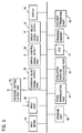
- the select control/calculation/display part 14 effects various kinds of control; for example, as depicted in Fig. 5, a CPU (Central Processing Unit) 31 reads out programs from a program memory 32 and interprets and executes instructions in the programs. Upon setting the receive frequency and the receive frequency bandwidth in input means 33, the CPU 31 sets the receive frequency f and the receive bandwidth of each of the receivers Rr and Rm via a receiver setting output part 34. The CPU 31 supplies an antenna select signal to each of the Wilkinson type power combiners SH1 to SH3 via an antenna select signal output part 35, enabling an arbitrary antenna element to be connected to the switch connected to the power combiner.
- a CPU Central Processing Unit
- the CPU 31 provides a switch control signal via a switch control signal output part 36 to each of the switches S1 to S3 to change over its connection. Furthermore, the CPU 31 applies a group select signal via a group select signal output part 37 to each of the Wilkinson type power combiners SHr and SHm to selectively output an arbitrary one of signals input thereinto.
- the measured data E(K, L) from the level calibrator 13 is input via an input part 38 into the select control/calculation/display part 14 and stored in its storage part 39.
- the select control/calculation/display part 14 further comprises a phase normalization part 41 for phase standardization of measured data, an evaluation function calculating part 42 for calculating the evaluation function V( ⁇ '), and a display 40 for displaying the calculated evaluation function.
- a hologram observation method will be described in connection with the case where a direct wave and an unstable reflected wave (reflected by a moving vehicle or the like and varying with time) are arriving from the directions of the antenna elements A5 and A3, respectively, as viewed from the center of array of antenna elements.
- the display 40 displays the evaluation function with the abscissa representing ⁇ ' and the ordinate V( ⁇ ').
- Fig. 7A shows the synthetic directional pattern of the antenna elements A2, A5 and A8, and Fig. 7B the synthetic directional pattern of the antenna elements A3, A4, A6 and A7.
- the direction of the main lobe BM is in the direction of arrival of the direct wave (i.e. the direction of the antenna element A5 as viewed from the center O of the circle of array of the antenna elements), and the null is in the direction of arrival of the reflected wave (the direction of the antenna element A3 as viewed from the center O of the circle).
- Steps (7) and (8) are to detect the phase difference between phase comparison reference signals measured with the above-mentioned two synthetic directional patterns, calculate one of the phase comparison reference signals and obtain the measured results of hologram observation based on the same phase reference.
- steps (1) to (9) By performing steps (1) to (9) repeatedly while scanning in the direction of the main lobe of the synthetic directional pattern for obtaining the phase comparison reference signal, hologram images of radio waves in plural directions of their arrival are observed, by which it is possible to evaluate an interference and/or disturbing wave and a multi-path reflected wave separately of each other. That is, steps (1) to (9) are performed, for example, after the direction of the main lobe held in the direction of the antenna element A5 by simultaneous selection of the antenna elements A2-A5-A8 and A3-A4-A6-A7, is switched to the direction of the antenna element A6 by simultaneous selection of A3-A6-A9 and A4-A5-A7-A8.
- steps (1) to (9) are similarly repeated while switching the direction of the main lobe of the synthetic directional pattern from one antenna element to another.
- a plurality of hologram images thus obtained are observed, and radio waves of varying relative levels are decided as interference and/or disturbing waves and radio waves with no variations in their relative levels are decided as a multi-path reflected waves.
- n is incremented by one, that is, the antenna elements simultaneously connected to the receiver Rr are shifted one by one, and if the calculated value is greater than the maximum value ⁇ RMAX , the latter is updated with the former and n is incremented by one. Then, the simultaneous connection of three antenna elements to the receiver Rr, the detection of the average received signal level, its comparison with the maximum value ⁇ RMAX and the one-by-one shifting of the three simultaneously selected antenna elements are repeated until n reaches the maximum value (24 in the example of Fig. 2). The direction of the antenna element A n+1 corresponding to the value n+1 at the time the maximum value ⁇ RMAX is obtained after the final processing is decided as the direction of arrival of the direct wave.
- Another method is to suitably select the antenna elements for connection to the receiver Rr, make hologram observations and selectively determine the direction of a stable radio wave of large level based on the results of observations.
- This method involves trials of combinations of antenna elements to be connected to the receiver Rr and the evaluation of temporal variations in receiving levels in plural observations that are carried out under the same condition.
- the measurable angular range by the directional pattern of one antenna element is approximately 120°.
- steps (1) to (9) are performed while changing the direction of the main lobe of the antenna directivity for obtaining the phase comparison reference signal through 120° at one time to make the measurement over the entire range of 360°, and steps (1) to (9) are performed at least three times every 120° to evaluate temporal variations of received signals.
- the direction of arrival of a stable radio wave is determined as the direction of the direct wave.
- the directions of arrival of the direct wave and the unstable reflected wave are detected, and the antenna elements are so selected as to obtain a synthetic directional pattern whose main lobe is directed in the direction of arrival of the direct wave and the null in the direction of the unstable reflected wave.
- stable hologram measurements are made possible by performing steps (1) to (9) using the received signal of the selectively combined antenna elements as the phase reference.
- the select control/calculation/display part 14 in Fig. 3 controls the antenna selection and receiver selection for performing steps (1) to (9), the antenna selection and receiver selection for determining the directions of arrival of the direct wave and the unstable reflected wave, make the correction in step (9) for the data E(K, L) obtained, conducts the calculation in step (9), and displays the calculated result using the set angle ⁇ ' as a parameter.
- the array antenna need not always be ring-shaped but it may also be such a circumferentially layered array antenna assembly as depicted in Fig. 8.
- steps (1) to (9) are performed for the array antenna of each layer to obtain data E( ⁇ , Z) (where Z represents the layer of the array antenna handled, the data E( ⁇ , Z) is read out of the storage part 43 and is Fourier transformed in the Fourier transform part 43 for Z.
- the Fourier-transformed result ⁇ ( ⁇ , ⁇ ) (where ⁇ is the elevation angle) is stored in the storage part 39.
- the antenna elements are selected prior to selecting the receiver to which the selected antenna elements are connected, but this order may be reversed.
- either one of the receivers Rr and Rm is selected for the application thereto of the received signal from each of the antenna elements A1 to A24 through one of receiver select switches S1 to S24, then Rr-side and Rm side change-over contacts r and m of the switches S1 to S24 are connected to the Wilkinson type power combiners SHr and SHm, respectively.
- the power combiner SHr selects the antenna elements in a manner to provide the reference synthetic directional pattern, and applies their received signals to the receiver Rr.
- the power combiner SHm selects the antenna elements one after another and applies its received signal to the receiver Rm.
- the process for the interference between the output from the receiver Rr and the output from the receiver Rm in the interferer 11 and the subsequent processes are the same as described previously with reference to Fig. 3.
- the Fig. 3 embodiment has an advantage over the Fig. 9 embodiment that the number of switches used is smaller than in the latter.
- the Wilkinson type power combiners SHr and SHm may be omitted, in which case the switches S1, S2 and S3 are connected at the contact r to the input of the receiver Rr and at the contact m to the input of the receiver Rm.
- the group select means can be dispensed with. In this instance, however, there is a fear that a signal input into the receiver Rr, for exampl, is reflected to the contact r of the switch S3 disconnected from the receiver Rr and then reflected by the contact r back to the receiver Rr.
- the number of antenna element groups is not limited specifically to three.
- the use of three or more receivers and simultaneous processing for the interference between the output from one reference fixed-reception receiver and the outputs from the other scanning-reception receivers could speed up the hologram observation.
- one or more of antenna elements of the array antenna are connected to the fixed-reception receiver, and its output is used as a reference received signal.
- the other antenna elements are selectively connected to the scanning-reception receiver one after another to provide equivalent rotation of the antenna for the interference between the received signal from each antenna element and the reference received signal.
- the rotation of the antenna can is faster than in the case of its mechanical driving for rotation, permitting reduction of the time for hologram observations.
- Stable measurements can be made by simultaneously selecting two or more antenna elements to set the main lobe of their synthetic directional pattern in direction of the direct wave.
- FIG. 10 Shown in Fig. 10 is an example of a dipole antenna that can be used as each of the antenna elements A1 to A24.
- Reference numeral 52 denotes a coaxial cable inserted through a hole made in a metal reflector 51 centrally thereof with its outer and central conductors 53 and 54 placed vertically to the reflector 51. The heights of the outer and central conductors 53 and 54 from the reflector surface are each set about a quarter wavelength.
- the outer conductor 53 has a pair of diametrically opposed slits 55 and 56 extending down from its top to the reflector 51; namely, the portion of the outer conductor 53 projecting upwardly of the reflector 51 is divided into two outer conductor pieces 53a and 53b.
- Reference numeral 57a denotes an antenna element connected at one end to the projecting end of the central conductor 54 and connected to the one outer conductor pieces 53a and held in parallel to the reflector 51. Aligned with the antenna element 57a is an antenna element 57b connected at one end to the other outer conductor piece 53b. The length of each of the antenna elements 57a and 57b is approximately ⁇ /4.
- the outer conductor 53 with the slits 55 and 56 equal to the ⁇ /4 length constitutes a balun (i.e., a balanced-to-unbalanced transformer).
- a balance radiation element of a dipole antenna 57 formed by the antenna elements 57a and 57b and an unbalanced feeder line of the coaxial cable 52 are balanced-to-unbalanced transform-connected, permitting therethrough of the passage of an unbalanced current (a common mode current) to the outside of the coaxial cable 52, thereby preventing unnecessary radiation.
- the antenna described above is produced by: making a hole in the reflector 51; inserting the coaxial cable 52 with the slits 55 and 56 through the hole and soldering the outer conductor 53 and the reflector 51; and soldering the antenna element 57a to the central conductor 54 and the outer conductor piece 53a and the antenna element 57b to the outer conductor piece 53b.
- the antenna of this example is not suitable for mass production. Furthermore, the soldering leads to variations in antenna characteristics, and during fabrication it is difficult to compensate for characteristic differences resulting from variations in properties of the materials used. To use this antenna as the may antenna element, it needs additional working for providing required element spacing, inevitably raising the manufacturing costs.
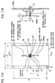
- a hollow, cylindrical feeding part 61 and first and second antenna parts 62 and 63 are formed in one piece of a synthetic resin material such as LCP (Liquid Crystal Polymer).
- the first and second antenna parts 62 and 63 each have a length nearly equal to a quarter of the wavelength ⁇ used.
- a reflector part 64 which is approximately ⁇ /4 away from the first and second antenna parts 62 and 63 and is substantially parallel thereto, is formed integrally with the feeding part 61.
- the feeding part 61 is located substantially at the center of the reflector part 64.
- the reflector part 64 may preferably be wide in area; for example, it is provided in a rectangular form measuring, for example, about ⁇ 3/4 by 2 ⁇ , and is placed with its longer sides held in parallel to the first and second antenna parts 62 and 63 (see Fig. 11).
- the first and second antenna parts 62 and 63 are given metal plating to form first and second antenna elements 65 and 66.
- the tubular feeding part 61 is coated over its interior surface with a metal-plated layer to form a metal-plated through hole 68.
- the through hole 68 is connected to the first antenna element 65 through a metal-plated coupling part 69.
- the feeding part 61 is coated over its exterior surface with a metal-plated layer to form an outer conductor 71, which has a pair of opposed slits 72 and 73 extending from the lower end face of the feeding part 61 toward the reflector part 64.
- the lengths of the slits 72 and 73 are shorter than the quarter wavelength, i.e. ⁇ /4.
- the reflector part 64 is coated over its external surface with a metal-plated reflector layer 74 and has a plurality of small holes (eight in this example) 75 bored at equiangular intervals about the feeding part 61.
- the interior surfaces of the small holes 75 are each covered with a metal-plated layer, forming a second through hole 76 that is contiguous to the reflector layer 74.
- the end portion of the feeding part 61 on the opposite side from the first and second antenna parts 62 and 63 forms a connector part 78, which is threaded around its outer peripheral surface and is given metal plating.
- the inner diameter of the connector part 78, defined by a stepped portion 79 formed therein, is larger than the inner diameter of the feeding part 61.
- the illustrated antenna is configures so that a plurality of such antennas can be combined into a ring-shaped may antenna.
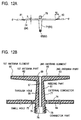
- the antenna of this example has coupling flanges 81 and 82 formed integrally with two opposite longer marginal edges of the reflector part 64 as depicted in Figs. 11A and 12A.
- the flanges 81 and 82 are each have a thickness about one-half of that of the reflector part 64.
- the flange 81 is flush with the one surface of he reflector part 64, whereas the flange 82 is flush with the other surface of the reflector part 64.
- the antenna is intended to enable such a ring-shaped array antenna as depicted in Fig.
- the flanges 81 and 82 are formed aslant in opposite directions at an angle ⁇ nearly equal to 7.5°.
- the flanges 81 and 82 are also given metal plating, and they have through holes 83 for joining means.
- a coaxial feeder line which has a characteristic impedance of, example, 50 ⁇ is formed by the through hole 68 serving as a center conductor and the outer conductor 71; the first and second antenna elements 65 and 66 form a half-wavelength dipole antenna; the reflector layer 74 forms a reflecting surface; and the slits 72 and 73 of the outer conductor 71, which are about ⁇ /4 long, form a balun (a balanced-to-unbalanced transformer).
- a dipole antenna is obtained which suppresses an unbalanced current. Since the through holes 76 formed by the small holes 75 are disposed around the feeding part 61 in close relation thereto, the through holes 76 serve as coaxial outer conductors in the reflector part 64, providing an excellent feeding part.
- the feeding part 61 In the manufacture of this antenna, the feeding part 61, as depicted in Fig. 13, a mold is used such that the first and second antenna parts 62 and 63, the reflector part 64, the connector part 78, and the coupling flanges 81-82 are formed in one piece of a synthetic resin material which is excellent in high-frequency characteristic and highly heat-resistant.
- the outer diameter of the feeding part 61 near the reflector part 64 is larger than its outer diameter near the first and second antenna elements 62 and 63, and the cross-sectional areas of the first and second antenna elements 62 and 63 are gradually decreased with distance from the feeding part 61.
- the marginal portions of the first and second antenna elements 62 and 63 facing toward the reflector part 64 are tapered and their marginal portions on the opposite side from the reflector part 64 are parallel therewith.
- the molded structure is coated all over its surface with a metal-plated layer.
- the metal-plated layer is provided by depositing, for example, copper (Cu) to a thickness of around 10 ⁇ m, then nickel (Ni) to a thickness of 5 ⁇ m, and gold (Au) to a thickness of 1 ⁇ m or less.
- the gold coating is intended for corrosion resistance.
- Such a composition of the metal-plated layer provides a good affinity for the molding of the synthetic resin material.
- the metal-plated layer on the end face of the feeding part 61 adjoining the first and second antenna parts 62 and 63 is selectively removed at the marginal edge diametrically opposite the first antenna part 62 across the through hole 67 to form an exposed part 84, thereby providing the first and second antenna elements 65 and 66.
- the plated layer deposited over the outer peripheral surface of the feeding part 61 is selectively removed to form the slits 72 and 73 which extend from the exposed part 84 of the end face of the feeding part 61 toward the reflector part 64 and are diametrically opposite across the through hole 67.
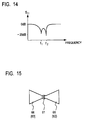
- an S parameter S 11 of this antenna is measured by a network analyzer or the like, and the lengths of the slits 72 and 73 are adjusted so that dip frequencies take desired values. That is, the frequency characteristic of the parameter S 11 exhibits a dip at a resonance frequency f 2 and at a lower frequency f 1 as depicted in Fig. 14.
- the frequency f 1 is an impedance matching point of the balun and the dipole antenna by the slits 72 and 73, and varies with the lengths of the slits 72 and 73. The more the frequency f 1 is spaced apart from the frequency f 2 , the wider the bandwidth of the antenna becomes but the higher the voltage standing wave ratio (VSWR).
- the frequency f 1 comes closer to f 2 .
- the lengths of the slits 72 and 73 are adjusted such that the frequency f 1 is, for example, 80% of the frequency f 2 , though it varies with the required value VSWR.
- the lengths of the slits 72 and 73 closer to ⁇ 0/(4& ⁇ r ) the frequency f 1 approaches f 2 . ( ⁇ 0: wavelength in free space)
- the angle ⁇ of each of the coupling flanges 81 and 82 is increased or decreased, depending on whether the number of antenna elements used is smaller or larger than 24.
- the angle ⁇ is zero, that is, the flanges 81 and 82 are parallel to the reflector part 64.
- the antenna can be made wide-band by making the first and second antenna elements 61 and 62 bow-shaped as depicted in Fig. 15.
- the reflector part 64 and the reflector layer 74 may be omitted.
- the above-described dipole antenna and the array antenna using such dipole antennas can be applied to other apparatus as well as the radio hologram observation apparatus.
- the dipole antenna of the present invention is manufactured by molding the antenna-forming parts in one piece, coating the molding with a metal-plated layer and removing a selected area of the layer--this permits mass production of antenna elements of close dimensional tolerances and hence of desired characteristics. Accordingly, the dipole antenna needs no additional working in the case of forming the array antenna.
- the dipole antenna of the present invention can be manufactured at low cost.
Landscapes
- Physics & Mathematics (AREA)
- General Physics & Mathematics (AREA)
- Variable-Direction Aerials And Aerial Arrays (AREA)
- Aerials With Secondary Devices (AREA)
Abstract
Description
- where:
- n and n' = 1, 2, ... , 24 (where 24 is the number of antenna elements)

Claims (19)
- A radio hologram observation apparatus comprising:an array antenna;a fixed-reception receiver and at least one scanning-reception receiver;antenna element selectively connecting means for selecting at least one of antenna elements of said array antenna and connecting said at least one antenna element to said fixed-reception receiver, and for selecting at least one of the other antenna elements and connecting said at least one antenna element to said scanning-reception receiver;data acquiring means for causing the output from said fixed-reception receiver and the output from said scanning-reception receiver to interfere with each other to obtain interference observation data; andcontrol means for obtaining said interference observation data from said data acquiring means by sequentially switching antenna elements for connection two said scanning-reception receiver while keeping connection of said at least one antenna element to said fixed-reception receiver
- The apparatus of claim 1, wherein said control means is means for switching said at least one antenna element connected to said fixed-reception receiver to another antenna element and obtaining second interference observation data while switching said at least one antenna element for connection to said scanning-reception receiver one after another, for calibrating said second interference observation data and said interference observation data on the basis of a common phase reference.
- The apparatus of claim 1, wherein: said antenna elements of said array antenna are divided into a plurality of groups; and said antenna element selectively connecting means comprises a plurality of antenna select means each of which has connected thereto said antenna elements of one of said plurality of groups, and a plurality of receiver select means for selectively connecting output terminals of said each antenna select means to said fixed-reception receiver and said scanning-reception receiver, said each antenna select means selecting one or more of said antenna elements of the group connected thereto and connecting them to said output terminals.
- The apparatus of claim 3, wherein each of said plurality of receiver select means comprises a plurality of change-over switches connected to the output terminals of said each antenna select means, and a plurality of group select means having their output terminals connected to input terminals of said fixed-reception and scanning-reception receivers and provided with a plurality of input terminals, and wherein each of said change-over switches is capable of selectively connecting output terminals of said antenna select means connected thereto to any one of said plurality of group select means through their different input terminals, and said each group select means is capable of selectively connecting one or more of its input terminals to its output terminal.
- The apparatus of claim 1, wherein said antenna element select means comprises a plurality of receiver select means connected to said antenna elements, respectively, and a plurality of antenna select means having their output terminals connected to input terminals of said fixed-reception and scanning-reception receivers and provided with input terminals of the same number as that of said antenna elements, and wherein each of said receiver select means is capable of selectively connecting said antenna elements connected thereto to the corresponding input terminals of said plurality of antenna select means, and each of said antenna select means is capable of connecting its one or more input terminals to its output terminal.
- The apparatus of claim 1, wherein said array antenna is formed with antenna elements arranged in a circumferentially layered form, said apparatus further comprising: means by which, letting the azimuth be represented by and the position in a direction parallel to the axis of said circumferentially layered form by Z, an interference observation value E(, Z) is Fourier transformed for Z to obtain Γ(, Ψ) (where Ψ is an elevation angle); and means by which, setting
- A radio hologram observation method comprising the steps of:(1) connecting at least one of antenna elements of an array antenna to a fixed-reception receiver, and sequentially connecting the other antenna elements of said array antenna to a scanning-reception receiver;(2) causing interference between the output from said fixed-reception receiver and the outputs from said scanning-reception receiver one after another to obtain a first sequence of interference observation data and storing it in storage means;(3) connecting a different antenna elements to said fixed-reception receiver; and(4) sequentially connecting the other antenna elements to said scanning-reception receiver and causing interference between the output from said fixed-reception receiver and the outputs from said scanning-reception receiver one after another to obtain a second sequence of interference observation data and storing it in storage means.
- The method of claim 7, further comprising the steps of:(5) connecting either one of said antenna element connected to said fixed-reception receiver in said step (1) and said antenna element connected to said fixed-reception receiver in said step (3) to said fixed-reception receiver and connecting the other antenna element to said scanning-reception receiver, and causing interference between the outputs from said fixed-reception and scanning-reception receivers to obtain interference observation data for calibration use; and(6) normalizing the phase of either one of said first and second sequences of interference observation data by said interference observation data for calibration use to make the phase references of said first and second sequences of interference observation data common to each other.
- The method of claim 8, wherein the number of antenna elements connected to said fixed-reception receiver in said sep (1) is plural, and a relatively narrow main lobe is formed in a synthetic antenna directional pattern of said plural antenna elements, and wherein the number of antenna elements connected to said fixed-reception receiver in said step (3) is plural, and a main lobe of a synthetic antenna directional pattern of said plural antenna elements lies in substantially the same direction as said main lobe.
- The method of claim 9, wherein said step (1) is preceded by a step of detecting the direction of arrival of a stable direct wave by means of said array antenna and at least said fixed-reception receiver and setting said main lobe in substantially the same direction as that of arrival of said direct wave.
- The method of claim 10, wherein: the antenna elements of said array antenna are divided into a plurality of groups; in said step (1),an antenna element in the direction of arrival of said direct wave and antenna elements on both sides of said antenna element in the same group are selectively connected to said fixed-reception receiver; and in said step (3), antenna elements of a group different from that of said antenna element in the direction of arrival of said direct wave and lying on both sides of said antenna element in the direction of said direction of arrival of direct wave are selectively connected to said fixed-reception receiver.
- The method of claim 8, wherein said array antenna is a ring-shaped one having a radius r, and wherein, letting the number of antenna elements of said array antenna be represented by N, the element number by n, the wavelength of the received radio wave by λ, and an equivalent radius taking into account the zenith angle by

- A dipole antenna comprising:a tubular feeding part and first and second antenna parts formed in one piece of an insulating material, said first and second antenna parts being extended from one end of said feeding part in opposite directions and having a length nearly equal to 1/4 of the effective wavelength λ;a first antenna element formed by a metal-plated layer all over said first antenna part and extending to the edge of a through hole of said feeding part;a second antenna element formed by a metal-plated layer all over said second antenna part;a through hole formed by a metal-plated layer deposited all over the interior surface of said through hole and connected to said first antenna element;an outer conductor formed by a metal-plated layer deposited all over the outer peripheral surface of said feeding part and connected to said first and second antenna elements; anda pair of slits cut in said outer conductor between said first and second antenna elements, said pair of slits extending a length about λ/4 from one end of said feeding part.
- The antenna of claim 13, further comprising: a reflector part formed integrally with said feeding part and said first and second antenna parts such that it is spaced about λ/4 apart from said first and second antenna parts of said feeding part, contiguous to or away from said pair of slits and substantially vertical to said feeding part and that said feeding part lies at the center of said reflector part; and a reflector layer formed by a metal-plated layer on either side of said reflector part and connected to said outer conductor.
- The antenna of claim 14, wherein said reflector part has a plurality of small holes bored therethrough around said feeding part, and said small holes forms second through holes connected to said reflector layer.
- The antenna of claim 14, wherein a connector is formed at the end portion of said feeding part on the opposite side from said first and second antenna parts.
- A dipole antenna manufacturing method comprising the steps of:forming a tubular feeding part, first and second antenna parts in one piece of an insulating material, said first and second antenna parts extending from one end of said feeding part in opposite directions and each having a length nearly equal to 1/4 of the effective wavelength λ, and said feeding part carring at the other end a connector part;depositing a metal-plated layer all over the surface of said one-piece structure and the interior surface of said feeding part;selectively removing said metal-plated layer on the end face of said one end of said feeding part on one side of its through hole to form an exposed part circularly arcuate about said through hole, and removing said metal-plated layer on the outer peripheral surface of said feeding part lengthwise thereof between said first and second antenna parts to form a pair of slits diametrically opposite across said through hole and each having a length nearly equal to λ/4; andremoving said metal-plated layer of said connector part between said metal-plated layer of said through hole and said metal-plated layer of said outer peripheral surface of said feeding part.
- The method of claim 17, wherein: during the formation of said one-piece structure a reflector part is formed integrally with said feeding part and said first and second antenna parts such that it is spaced about λ/4 apart from said first and second antenna parts of said feeding part, contiguous to or away from said pair of slits and substantially vertical to said feeding part and that said feeding part lies at the center of said reflector part; during the formation of said one-piece structure a plurality of small through holes are made in said reflector part around said feeding part; and during the formation of said metal-plated layer the interior surfaces of said small through holes are also given metal plating.
- The method of claim 18, wherein an S-parameter of said antenna is measured and the lengths of said pair of slits are adjusted so that its dip-point frequency takes a desired value.
Priority Applications (1)
| Application Number | Priority Date | Filing Date | Title |
|---|---|---|---|
| EP08004541A EP1933209A3 (en) | 1999-04-19 | 2000-04-19 | Dipole antenna and method of manufacturing the same |
Applications Claiming Priority (4)
| Application Number | Priority Date | Filing Date | Title |
|---|---|---|---|
| JP11033499A JP2000307329A (en) | 1999-04-19 | 1999-04-19 | Dipole antenna and method of manufacturing the same |
| JP11033499 | 1999-04-19 | ||
| JP16648599 | 1999-06-14 | ||
| JP16648599A JP3753296B2 (en) | 1999-06-14 | 1999-06-14 | Radio hologram observation device |
Related Child Applications (1)
| Application Number | Title | Priority Date | Filing Date |
|---|---|---|---|
| EP08004541A Division EP1933209A3 (en) | 1999-04-19 | 2000-04-19 | Dipole antenna and method of manufacturing the same |
Publications (2)
| Publication Number | Publication Date |
|---|---|
| EP1046962A2 true EP1046962A2 (en) | 2000-10-25 |
| EP1046962A3 EP1046962A3 (en) | 2002-05-08 |
Family
ID=26449981
Family Applications (2)
| Application Number | Title | Priority Date | Filing Date |
|---|---|---|---|
| EP00108558A Withdrawn EP1046962A3 (en) | 1999-04-19 | 2000-04-19 | Radio hologram observation apparatus and method therefor |
| EP08004541A Withdrawn EP1933209A3 (en) | 1999-04-19 | 2000-04-19 | Dipole antenna and method of manufacturing the same |
Family Applications After (1)
| Application Number | Title | Priority Date | Filing Date |
|---|---|---|---|
| EP08004541A Withdrawn EP1933209A3 (en) | 1999-04-19 | 2000-04-19 | Dipole antenna and method of manufacturing the same |
Country Status (2)
| Country | Link |
|---|---|
| US (2) | US6275181B1 (en) |
| EP (2) | EP1046962A3 (en) |
Cited By (3)
| Publication number | Priority date | Publication date | Assignee | Title |
|---|---|---|---|---|
| EP1291972A1 (en) * | 2001-08-30 | 2003-03-12 | S.O. Solo Enterprise Ltd. | Radioholographic aerials apparatus and method therefor |
| EP3236532A1 (en) * | 2016-04-21 | 2017-10-25 | The Boeing Company | Dynamically allocated broad band multi-tap antenna |
| CN112635976A (en) * | 2020-12-17 | 2021-04-09 | 中北大学南通智能光机电研究院 | Zigzag dipole 5G base station antenna unit |
Families Citing this family (21)
| Publication number | Priority date | Publication date | Assignee | Title |
|---|---|---|---|---|
| ATE360268T1 (en) * | 2002-12-23 | 2007-05-15 | Huber+Suhner Ag | BROADBAND ANTENNA WITH A 3-DIMENSIONAL CASTING |
| GB0701090D0 (en) * | 2007-01-19 | 2007-02-28 | Plasma Antennas Ltd | A selectable beam antenna |
| EP2171798A1 (en) * | 2007-07-24 | 2010-04-07 | Thomson Licensing | Multi-antenna system feed device and wireless link terminal equipped with such a device. |
| JP5208547B2 (en) * | 2008-03-19 | 2013-06-12 | 東京エレクトロン株式会社 | Power combiner and microwave introduction mechanism |
| FR2942914A1 (en) | 2009-03-06 | 2010-09-10 | Alcatel Lucent | DEVICE FOR ASSEMBLING AN ANTENNA |
| FR2957194B1 (en) * | 2010-03-04 | 2012-03-02 | Tdf | ANTENNAIRE STRUCTURE WITH DIPOLES |
| TWI452861B (en) * | 2010-10-08 | 2014-09-11 | Realtek Semiconductor Corp | Antenna diversity apparatus and antenna diversity method |
| AU2011314378A1 (en) | 2010-10-15 | 2013-05-02 | Searete Llc | Surface scattering antennas |
| US9385435B2 (en) | 2013-03-15 | 2016-07-05 | The Invention Science Fund I, Llc | Surface scattering antenna improvements |
| CN103259102A (en) * | 2013-05-06 | 2013-08-21 | 重庆金美通信有限责任公司 | A Smart Antenna with Omnidirectional Coverage |
| US9923271B2 (en) | 2013-10-21 | 2018-03-20 | Elwha Llc | Antenna system having at least two apertures facilitating reduction of interfering signals |
| US9935375B2 (en) | 2013-12-10 | 2018-04-03 | Elwha Llc | Surface scattering reflector antenna |
| US9825358B2 (en) | 2013-12-17 | 2017-11-21 | Elwha Llc | System wirelessly transferring power to a target device over a modeled transmission pathway without exceeding a radiation limit for human beings |
| US9843103B2 (en) | 2014-03-26 | 2017-12-12 | Elwha Llc | Methods and apparatus for controlling a surface scattering antenna array |
| US9853361B2 (en) | 2014-05-02 | 2017-12-26 | The Invention Science Fund I Llc | Surface scattering antennas with lumped elements |
| US10446903B2 (en) | 2014-05-02 | 2019-10-15 | The Invention Science Fund I, Llc | Curved surface scattering antennas |
| US9882288B2 (en) | 2014-05-02 | 2018-01-30 | The Invention Science Fund I Llc | Slotted surface scattering antennas |
| US10178560B2 (en) | 2015-06-15 | 2019-01-08 | The Invention Science Fund I Llc | Methods and systems for communication with beamforming antennas |
| US10361481B2 (en) | 2016-10-31 | 2019-07-23 | The Invention Science Fund I, Llc | Surface scattering antennas with frequency shifting for mutual coupling mitigation |
| US10948578B2 (en) * | 2018-10-10 | 2021-03-16 | International Business Machines Corporation | Distinguishing holographic objects from physical objects |
| JP7210408B2 (en) * | 2019-09-13 | 2023-01-23 | 株式会社東芝 | Electronic device and method |
Family Cites Families (16)
| Publication number | Priority date | Publication date | Assignee | Title |
|---|---|---|---|---|
| US2462881A (en) * | 1943-10-25 | 1949-03-01 | John W Marchetti | Antenna |
| US2976534A (en) * | 1959-07-02 | 1961-03-21 | Kampinsky Abe | Circularly polarized antenna |
| US3681771A (en) * | 1970-03-23 | 1972-08-01 | Macdowell Associates Inc | Retroflector dipole antenna array and method of making |
| US3887923A (en) * | 1973-06-26 | 1975-06-03 | Us Navy | Radio-frequency holography |
| US3922683A (en) * | 1974-06-24 | 1975-11-25 | Hazeltine Corp | Three frequency band antenna |
| US4647942A (en) * | 1981-11-20 | 1987-03-03 | Western Geophysical Co. | Circularly polarized antenna for satellite positioning systems |
| WO1988006295A1 (en) * | 1987-02-13 | 1988-08-25 | Mitsubishi Denki Kabushiki Kaisha | Holographic radar |
| US5216695A (en) * | 1991-06-14 | 1993-06-01 | Anro Engineering, Inc. | Short pulse microwave source with a high prf and low power drain |
| US5283590A (en) * | 1992-04-06 | 1994-02-01 | Trw Inc. | Antenna beam shaping by means of physical rotation of circularly polarized radiators |
| US5748156A (en) * | 1994-02-28 | 1998-05-05 | Chaparral Communications | High-performance antenna structure |
| JPH09153725A (en) * | 1995-11-30 | 1997-06-10 | Advantest Corp | Probe antenna |
| IL123364A (en) * | 1997-02-20 | 2003-07-06 | Advantest Corp | Hologram observation method for three-dimensional wave source distribution, and stereoscopic directivity estimation method of antenna and wave distribution observation method based on hologram observation |
| US6111549A (en) * | 1997-03-27 | 2000-08-29 | Satloc, Inc. | Flexible circuit antenna and method of manufacture thereof |
| US6198539B1 (en) * | 1997-08-22 | 2001-03-06 | Advantest Corporation | Hologram observation method and hologram observation apparatus |
| US6188356B1 (en) * | 1998-05-12 | 2001-02-13 | Advantest Corporation | Radio monitoring method and apparatus |
| AUPP549598A0 (en) * | 1998-08-27 | 1998-09-17 | Alcatel Alsthom Compagnie Generale D'electricite | Dipole feed arrangement for a reflector antenna |
-
2000
- 2000-04-18 US US09/551,099 patent/US6275181B1/en not_active Expired - Fee Related
- 2000-04-19 EP EP00108558A patent/EP1046962A3/en not_active Withdrawn
- 2000-04-19 EP EP08004541A patent/EP1933209A3/en not_active Withdrawn
-
2001
- 2001-03-30 US US09/823,392 patent/US6400331B2/en not_active Expired - Fee Related
Cited By (4)
| Publication number | Priority date | Publication date | Assignee | Title |
|---|---|---|---|---|
| EP1291972A1 (en) * | 2001-08-30 | 2003-03-12 | S.O. Solo Enterprise Ltd. | Radioholographic aerials apparatus and method therefor |
| EP3236532A1 (en) * | 2016-04-21 | 2017-10-25 | The Boeing Company | Dynamically allocated broad band multi-tap antenna |
| US9985352B2 (en) | 2016-04-21 | 2018-05-29 | The Boeing Company | Dynamically allocated broadband multi-tap antenna |
| CN112635976A (en) * | 2020-12-17 | 2021-04-09 | 中北大学南通智能光机电研究院 | Zigzag dipole 5G base station antenna unit |
Also Published As
| Publication number | Publication date |
|---|---|
| US20010022561A1 (en) | 2001-09-20 |
| EP1933209A3 (en) | 2008-07-16 |
| US6275181B1 (en) | 2001-08-14 |
| EP1933209A2 (en) | 2008-06-18 |
| US6400331B2 (en) | 2002-06-04 |
| EP1046962A3 (en) | 2002-05-08 |
Similar Documents
| Publication | Publication Date | Title |
|---|---|---|
| US6275181B1 (en) | Radio hologram observation apparatus and method therefor | |
| EP0469741B1 (en) | Radio frequency apparatus | |
| US10424836B2 (en) | Horizon nulling helix antenna | |
| EP1811601B1 (en) | An antenna | |
| US10483631B2 (en) | Decoupled concentric helix antenna | |
| Syrytsin et al. | Compact quad-mode planar phased array with wideband for 5G mobile terminals | |
| US6160523A (en) | Crank quadrifilar slot antenna | |
| US9281564B2 (en) | Systems and methods for providing directional radiation fields using distributed loaded monopole antennas | |
| US8044864B2 (en) | Antenna and associated measurement sensor | |
| KR100709688B1 (en) | Antenna manufacture | |
| US20100225554A1 (en) | Balanced Metamaterial Antenna Device | |
| DK176727B1 (en) | Circularly polarized antennas | |
| USRE42087E1 (en) | Tunable antenna system | |
| JPWO2003021824A1 (en) | Wireless terminal test equipment using a single self-complementary antenna | |
| CA2030886C (en) | Microstrip antenna of two-frequency separate-feeding type for circularly polarized waves | |
| JPWO2000069022A1 (en) | circularly polarized antenna | |
| CN112134004B (en) | A Wide-beam Quadruple Helix Antenna with Equal-flux Radiation Characteristics | |
| CA2248853A1 (en) | Helix antenna with a built-in broadband power supply, and manufacturing methods therefor | |
| US6288686B1 (en) | Tapered direct fed quadrifilar helix antenna | |
| US20170062917A1 (en) | Multi-filar helical antenna | |
| KR101409768B1 (en) | Multi-band gps attenna | |
| JP4136178B2 (en) | Twin loop antenna | |
| CN102089929A (en) | A dielectrically-loaded antenna | |
| Row et al. | Direction of arrival estimation system based on a vertically-polarized circular array with 360 continuous null steering | |
| CN109546301A (en) | A kind of satellite navigation reception two-fold arm four-arm spiral antenna of miniaturization |
Legal Events
| Date | Code | Title | Description |
|---|---|---|---|
| PUAI | Public reference made under article 153(3) epc to a published international application that has entered the european phase |
Free format text: ORIGINAL CODE: 0009012 |
|
| 17P | Request for examination filed |
Effective date: 20000419 |
|
| AK | Designated contracting states |
Kind code of ref document: A2 Designated state(s): AT BE CH CY DE DK ES FI FR GB GR IE IT LI LU MC NL PT SE |
|
| AX | Request for extension of the european patent |
Free format text: AL;LT;LV;MK;RO;SI |
|
| RIC1 | Information provided on ipc code assigned before grant |
Free format text: 7G 03H 5/00 A, 7H 01Q 1/38 B |
|
| PUAL | Search report despatched |
Free format text: ORIGINAL CODE: 0009013 |
|
| AK | Designated contracting states |
Kind code of ref document: A3 Designated state(s): AT BE CH CY DE DK ES FI FR GB GR IE IT LI LU MC NL PT SE |
|
| AX | Request for extension of the european patent |
Free format text: AL;LT;LV;MK;RO;SI |
|
| AKX | Designation fees paid |
Designated state(s): DE FR GB |
|
| RAP1 | Party data changed (applicant data changed or rights of an application transferred) |
Owner name: ADVANTEST CORPORATION Owner name: MINISTRY FOR PUBLIC MANAGEMENT, HOME AFFAIRS, POST |
|
| RAP1 | Party data changed (applicant data changed or rights of an application transferred) |
Owner name: MINISTRY OF INTERNAL AFFAIRS AND COMMUNICATIONS Owner name: ADVANTEST CORPORATION |
|
| 17Q | First examination report despatched |
Effective date: 20071109 |
|
| STAA | Information on the status of an ep patent application or granted ep patent |
Free format text: STATUS: THE APPLICATION IS DEEMED TO BE WITHDRAWN |
|
| 18D | Application deemed to be withdrawn |
Effective date: 20091031 |