EP1046462B1 - Wafer holding plate for wafer grinding apparatus and method for manufacturing the same. - Google Patents
Wafer holding plate for wafer grinding apparatus and method for manufacturing the same. Download PDFInfo
- Publication number
- EP1046462B1 EP1046462B1 EP00302282A EP00302282A EP1046462B1 EP 1046462 B1 EP1046462 B1 EP 1046462B1 EP 00302282 A EP00302282 A EP 00302282A EP 00302282 A EP00302282 A EP 00302282A EP 1046462 B1 EP1046462 B1 EP 1046462B1
- Authority
- EP
- European Patent Office
- Prior art keywords
- wafer
- grooves
- substrate
- holding plate
- wafer holding
- Prior art date
- Legal status (The legal status is an assumption and is not a legal conclusion. Google has not performed a legal analysis and makes no representation as to the accuracy of the status listed.)
- Expired - Lifetime
Links
Images



Classifications
-
- B—PERFORMING OPERATIONS; TRANSPORTING
- B24—GRINDING; POLISHING
- B24B—MACHINES, DEVICES, OR PROCESSES FOR GRINDING OR POLISHING; DRESSING OR CONDITIONING OF ABRADING SURFACES; FEEDING OF GRINDING, POLISHING, OR LAPPING AGENTS
- B24B37/00—Lapping machines or devices; Accessories
- B24B37/27—Work carriers
- B24B37/30—Work carriers for single side lapping of plane surfaces
-
- B—PERFORMING OPERATIONS; TRANSPORTING
- B24—GRINDING; POLISHING
- B24B—MACHINES, DEVICES, OR PROCESSES FOR GRINDING OR POLISHING; DRESSING OR CONDITIONING OF ABRADING SURFACES; FEEDING OF GRINDING, POLISHING, OR LAPPING AGENTS
- B24B7/00—Machines or devices designed for grinding plane surfaces on work, including polishing plane glass surfaces; Accessories therefor
- B24B7/20—Machines or devices designed for grinding plane surfaces on work, including polishing plane glass surfaces; Accessories therefor characterised by a special design with respect to properties of the material of non-metallic articles to be ground
- B24B7/22—Machines or devices designed for grinding plane surfaces on work, including polishing plane glass surfaces; Accessories therefor characterised by a special design with respect to properties of the material of non-metallic articles to be ground for grinding inorganic material, e.g. stone, ceramics, porcelain
- B24B7/228—Machines or devices designed for grinding plane surfaces on work, including polishing plane glass surfaces; Accessories therefor characterised by a special design with respect to properties of the material of non-metallic articles to be ground for grinding inorganic material, e.g. stone, ceramics, porcelain for grinding thin, brittle parts, e.g. semiconductors, wafers
-
- B—PERFORMING OPERATIONS; TRANSPORTING
- B24—GRINDING; POLISHING
- B24C—ABRASIVE OR RELATED BLASTING WITH PARTICULATE MATERIAL
- B24C1/00—Methods for use of abrasive blasting for producing particular effects; Use of auxiliary equipment in connection with such methods
- B24C1/04—Methods for use of abrasive blasting for producing particular effects; Use of auxiliary equipment in connection with such methods for treating only selected parts of a surface, e.g. for carving stone or glass
-
- B—PERFORMING OPERATIONS; TRANSPORTING
- B24—GRINDING; POLISHING
- B24C—ABRASIVE OR RELATED BLASTING WITH PARTICULATE MATERIAL
- B24C3/00—Abrasive blasting machines or devices; Plants
- B24C3/32—Abrasive blasting machines or devices; Plants designed for abrasive blasting of particular work, e.g. the internal surfaces of cylinder blocks
- B24C3/322—Abrasive blasting machines or devices; Plants designed for abrasive blasting of particular work, e.g. the internal surfaces of cylinder blocks for electrical components
Definitions
- the present invention relates to a wafer holding plate used for wafer grinding apparatuses and a method for manufacturing the same.
- a typical wafer grinding apparatus includes a table, which is fixed to a cooling jacket, and a wafer holding plate.
- the plate has a wafer adhering surface to which an adhesive, such as a thermoplastic wax, is applied.
- the adhesive attaches a semiconductor wafer to the plate.
- the adhesive Since the wafer adhering surface is flat, the adhesive must be relatively thick to ensure adhesion of the semiconductor wafer. It is difficult to apply the adhesive uniformly. As a result, parallelism between the wafer adhering surface and the semiconductor wafer is not achieved, which causes the semiconductor wafer to be held obliquely. Therefore, it is difficult to achieve highly accurate grinding.
- the lands and pits of the plate surface are transferred to the rear surface of the wafer (the surface adhered to the plate) when the plate holding the wafer is pressed against a grinding surface. This decreases the accuracy and quality of the semiconductor wafer. Additionally, production efficiency decreases because wafers have to be reground to correct dimensions.
- EP-A-1020253 (prior art document according to Article 54(3)EPC) discloses a wafer holding plate having a roughness of 0.5 ⁇ m to 1.5 ⁇ m.
- the present invention provides a wafer holding plate used in a wafer grinding apparatus, including a wafer holding plate used in a wafer grinding apparatus including a substrate having a wafer adhering surface to which a semiconductor wafer can be adhered by an adhesive, characterised in that the wafer adhering surface has a groove pattern formed thereon and a surface roughness Ra of no greater than 0.1 ⁇ m.
- Fig. 1 is a schematic view showing a wafer grinding apparatus 1 according to a first embodiment of the present invention.
- the wafer grinding apparatus 1 is a lapping machine for grinding a wafer slice. The wafer was sliced during a bare wafer process. Further, the wafer grinding apparatus 1 includes a round metal table 2, which is preferably made of stainless steel or the like.
- the table 2 has an upper surface, or grinding surface 2a, on which the semiconductor wafer 5 is ground. A grinding cloth (not shown) is adhered to the grinding surface 2a.
- the table 2 is fastened to a round cooling jacket 3 by bolts (not shown).
- the cooling jacket 3 is supported horizontally by a cylindrical rotary shaft 4. Coolant W circulates through a flow passage extending through the interior of the cooling jacket 3.
- the wafer grinding apparatus 1 has a plurality of (e.g., two) wafer holding plates 6 (also known as pusher plates, only one shown). Each of the wafer holding plates 6 is formed from a circular substrate B1.
- the substrate B1 has an upper surface 6b, the center of which is fixed to a pusher rod 7 of a drive apparatus (not shown).
- a wafer adhering surface 6a is on the opposite, lower side of the substrate B1 and faces the grinding surface 2a of the table 2.
- the pusher rod 7 supports the wafer holding plate 6 so that the wafer adhering surface 6a is parallel to the grinding surface 2a.
- Each pusher rod 7 rotates integrally with the associated plate 6 and moves vertically within a predetermined range.
- a plurality of semiconductor wafers 5 are adhered to the wafer adhering surface 6a of the plate 6 by a thermoplastic wax 8.
- the front surface of each wafer 5 faces the grinding surface 2a.
- the wafer grinding apparatus 1 presses the plate 6 against the grinding surface 2a with a predetermined force so that the wafers 5 contact the grinding surface 2a.
- the wafer holding plates 6 be formed from a sintered ceramic body. Further, it is preferred that the sintered ceramic body have a high density and be made of a material such as sintered ceramic silicide or sintered ceramic carbide. In the first embodiment, the wafer holding plates 6 are formed from a sintered silicon carbide (SiC) body.
- SiC sintered silicon carbide
- the preferred density of the sintered ceramic body is 2.7g/cm 3 or higher. It is more preferred that the density be 3.0g/cm 3 or higher and most preferred that the density be 3.1g/cm 3 or higher. This is because the thermal conductivity increases when the density of the sintered body increases.
- the preferred thermal conductivity is 30W/mK or higher. It is more preferred that the thermal conductivity be within the range of 80W/mK to 200W/mK. If the thermal conductivity is too low, it is difficult to keep the temperature of the sintered body uniform. A non-uniform temperature limits accuracy and quality and hinders manufacture of semiconductor wafers 5 that have a large diameter. On the other hand, it is difficult to find stable, inexpensive materials that have a thermal conductivity higher than 200W/mK.
- the wafer adhering surface 6a is a mirror-like surface having a surface roughness Ra of 0.1 ⁇ m or less.
- An anchoring groove pattern 10 is formed in the wafer adhering surface 6a.
- the anchoring groove pattern 10 includes a plurality of straight grooves 9.
- the grooves 9 are equally spaced from one another and arranged in a grid-like manner.
- the groove pattern 10 is formed by intersecting a plurality of the grooves 9 with each other. It is preferred that the grooves 9 occupy about 1% to 50% of the wafer adhering surface 6a. It is further preferred that the grooves 9 occupy about 1% to 20% of the adhering surface 6a.
- the width of the grooves be about 50 ⁇ m to 500 ⁇ m. If the width is less than 50 ⁇ m, the wax 8 cannot be properly anchored to the adhering surface 6a. This makes it difficult to apply the wax 8 uniformly, which in turn, makes it difficult to improve wafer parallelism. On the other hand, if the width exceeds 500 ⁇ m, the pits and lands formed by the grooves 9 may be transferred to the wafers 5 and affect the quality of the wafers 5.
- the grooves 9 have a depth of about 20 ⁇ m to 100 ⁇ m. If the depth of the grooves 9 is less than 20 ⁇ m, the grooves 9 may not properly function as anchors. On the other hand, if the depth of the grooves 9 exceeds 100 ⁇ m, pits and lands formed by the grooves 9 may be transferred to the wafers 5.
- a plate-like substrate B1 is first prepared.
- the preferred embodiment uses "SC-850" which is a dense sintered silicon carbide body produced by IBIDEN KABUSHIKI KAISHA.
- the sintered body has a density of 3.1 g/cm 3 and a thermal conductivity of 150W/mK.
- the substrate B1 may be formed from a dense sintered ceramic body produced through a normal procedure during which a ceramic raw material forming step, a molding step, and a baking step are sequentially performed.
- the wafer adhering surface 6a of the substrate B1 is then ground to obtain a mirror-like surface, the surface roughness Ra of which is 0.1 ⁇ m or less.
- the surface grinding is performed by using a hard silicon carbide grinding fixture.
- the wafer adhering surface 6a is sandblasted.
- a mask 11 is used in the sandblasting to form the grooves 9. The sandblasting process will now be discussed with reference to Figs. 4(a) to 4(c).
- the mask 11 which is grid-like to conform with the groove pattern 10, is applied to the wafer adhering surface 6a.
- the mask 11 exposes the locations of the grooves 9 to abrasive grains 14 and protects other parts of the wafer adhering surface 6a from the abrasive grains 14.
- a photosensitive resin R1 is uniformly applied to the substrate B1. Ultraviolet rays are then irradiated toward the photosensitive resin R1 through a photomask 12 to selectively expose portions corresponding to the grooves 9 to the ultraviolet rays (Fig. 4(a)).
- An urethane or acrylic resin having photosensitivity may be used as the photosensitive resin R1.
- the photosensitive resin R1 is developed, washed, and dried. Afterward, the unexposed portions of the photosensitive resin R1 are removed to form slits 13 (Fig. 4(b)).
- the mask 11 When an indirect printing method is employed to form the mask 11, a film mask 11 having the slits 13 is positioned on and adhered to the wafer adhering surface 6a of the substrate B1. Regardless of the printing method, the mask 11 is required to have a thickness that can resist sandblasting. More specifically, it is preferred that the mask 11 have a thickness of 50 ⁇ m to 300 ⁇ m.
- the abrasive grains 14 are blasted against the substrate B1 from a nozzle 15 (Fig. 4(c)).
- the blasted abrasive grains 14 etch the wafer adhering surface 6a and form the grooves 9, which have the predetermined width and depth at positions corresponding to the slits 13. After the sandblasting process, the mask 11 is removed and the wafer holding plate 6 is completed.
- Fig. 5 is a cross-sectional view showing a wafer holding plate 60 not falling within the scope of the present invention.
- the wafer holding plate 60 includes a substrate B1 having a mirror-like surface 60a.
- An anchoring groove pattern 10 is formed in the mirror-like surface 60a.
- the anchoring groove pattern 10 includes a plurality of generally V-shaped grooves 90. As shown in Figs. 5 and 6(d), the edges of the grooves 90 are curved. That is, the edges of the grooves 90 are not squared. Further, the grooves 90 each have a rounded bottom surface. In other words, the edges and the walls of each groove do not have angled surfaces where internal stress would concentrate.
- the grooves 90 are formed by applying the mask 11 to the substrate B1 and sandblasting abrasive grains 14 from the nozzle 15 against the substrate B1.
- the amount of abrasive grains 14 blasted against a first portion of the substrate B1, which is located directly below the nozzle 15, is greater than that blasted against the portions adjacent to the first portion, or a second portion of the substrate B2.
- the first portion is etched at a faster speed than the second portion.
- the bottom of each groove 90 is formed at the location corresponding to the first portion as shown in Fig. 6(d).
- the abrasive grains 14 form edges that are curved and not squared. In other words, when the wafer adhering surface 6a is sandblasted, formation of the grooves 90 and the rounding of the groove edges are performed simultaneously.
- the edges of the grooves 90 in the groove pattern 10 of each wafer holding plate 60 are rounded. Since the grooves 90 do not have squared edges, the groove edges are less likely to break. Accordingly, there are no places where particles are likely to break apart from the grooves 10. Therefore, lands and pits are not transferred to the wafers 5. Thus, the wafers 5 are neither scratched nor damaged. Since correction of transferred lands and pits is not needed, the manufacturing efficiency is improved.
- the formation and rounding of the grooves 90 are performed simultaneously. Accordingly, the grooves 90 having curved edges are formed within a short period of time.
- the plates 6 are thus formed inexpensively and efficiently.
Landscapes
- Engineering & Computer Science (AREA)
- Mechanical Engineering (AREA)
- Chemical & Material Sciences (AREA)
- Ceramic Engineering (AREA)
- Inorganic Chemistry (AREA)
- Mechanical Treatment Of Semiconductor (AREA)
- Finish Polishing, Edge Sharpening, And Grinding By Specific Grinding Devices (AREA)
Description
- The present invention relates to a wafer holding plate used for wafer grinding apparatuses and a method for manufacturing the same.
- Apparatuses for grinding the surface of a semiconductor wafer, such as a lapping machine or a polishing machine, are known in the prior art. A typical wafer grinding apparatus includes a table, which is fixed to a cooling jacket, and a wafer holding plate. The plate has a wafer adhering surface to which an adhesive, such as a thermoplastic wax, is applied. The adhesive attaches a semiconductor wafer to the plate.
- Since the wafer adhering surface is flat, the adhesive must be relatively thick to ensure adhesion of the semiconductor wafer. It is difficult to apply the adhesive uniformly. As a result, parallelism between the wafer adhering surface and the semiconductor wafer is not achieved, which causes the semiconductor wafer to be held obliquely. Therefore, it is difficult to achieve highly accurate grinding.
- Furthermore, if the surface of the plate is rough, the lands and pits of the plate surface are transferred to the rear surface of the wafer (the surface adhered to the plate) when the plate holding the wafer is pressed against a grinding surface. This decreases the accuracy and quality of the semiconductor wafer. Additionally, production efficiency decreases because wafers have to be reground to correct dimensions.
- EP-A-1020253 (prior art document according to Article 54(3)EPC) discloses a wafer holding plate having a roughness of 0.5µm to 1.5µm.
- It is an object of the present invention to provide a wafer holding plate for a wafer grinding apparatus that can manufacture a semiconductor wafer with high accuracy and high quality.
- To achieve the above object, the present invention provides a wafer holding plate used in a wafer grinding apparatus, including a wafer holding plate used in a wafer grinding apparatus including a substrate having a wafer adhering surface to which a semiconductor wafer can be adhered by an adhesive, characterised in that the wafer adhering surface has a groove pattern formed thereon and a surface roughness Ra of no greater than 0.1µm.
- Other aspects and advantages of the present invention will become apparent from the following description, taken in conjunction with the accompanying drawings, illustrating by way of example the principles of the invention.
- The invention and preferred objects and advantages thereof, may best be understood by reference to the following description of the certain exemplifying preferred embodiments together with the accompanying drawings in which:
- Fig. 1 is a schematic diagram showing a wafer grinding apparatus according to an of the present invention;
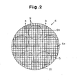
- Fig. 2 is a schematic plan view showing a wafer holding plate of the apparatus of Fig. 1;
- Fig. 3 is a schematic cross-sectional view taken along line 3-3 in Fig. 2;
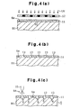
- Figs. 4(a) to 4(c) are schematic cross-sectional views illustrating the procedures for manufacturing the plate of Fig. 2;
- Fig. 5 is a schematic cross-sectional view showing a wafer holding plate not falling within the scope of the present invention;
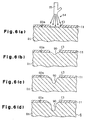
- Figs. 6(a) to 6(d) are schematic cross-sectional views illustrating the procedures for manufacturing the plate of Fig. 5;
- Fig. 7 is a schematic cross-sectional view showing a wafer holding plate according to a second embodiment of the present invention;
- Fig. 8 is a schematic cross-sectional view showing a wafer holding plate according to a third embodiment of the present invention; and
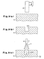
- Figs. 9(a) to 9(c) are schematic cross-sectional views showing the procedures for manufacturing the plate of Fig. 5.
-
- In the drawings, like numerals are used for like elements throughout.
- Fig. 1 is a schematic view showing a wafer grinding apparatus 1 according to a first embodiment of the present invention. The wafer grinding apparatus 1 is a lapping machine for grinding a wafer slice. The wafer was sliced during a bare wafer process. Further, the wafer grinding apparatus 1 includes a round metal table 2, which is preferably made of stainless steel or the like. The table 2 has an upper surface, or grinding
surface 2a, on which thesemiconductor wafer 5 is ground. A grinding cloth (not shown) is adhered to thegrinding surface 2a. The table 2 is fastened to around cooling jacket 3 by bolts (not shown). Thecooling jacket 3 is supported horizontally by a cylindrical rotary shaft 4. Coolant W circulates through a flow passage extending through the interior of thecooling jacket 3. - The wafer grinding apparatus 1 has a plurality of (e.g., two) wafer holding plates 6 (also known as pusher plates, only one shown). Each of the
wafer holding plates 6 is formed from a circular substrate B1. The substrate B1 has anupper surface 6b, the center of which is fixed to apusher rod 7 of a drive apparatus (not shown). Awafer adhering surface 6a is on the opposite, lower side of the substrate B1 and faces thegrinding surface 2a of the table 2. Thepusher rod 7 supports thewafer holding plate 6 so that thewafer adhering surface 6a is parallel to thegrinding surface 2a. Eachpusher rod 7 rotates integrally with the associatedplate 6 and moves vertically within a predetermined range. A plurality ofsemiconductor wafers 5 are adhered to thewafer adhering surface 6a of theplate 6 by athermoplastic wax 8. The front surface of eachwafer 5 faces thegrinding surface 2a. The wafer grinding apparatus 1 presses theplate 6 against thegrinding surface 2a with a predetermined force so that thewafers 5 contact thegrinding surface 2a. - It is preferred that the
wafer holding plates 6 be formed from a sintered ceramic body. Further, it is preferred that the sintered ceramic body have a high density and be made of a material such as sintered ceramic silicide or sintered ceramic carbide. In the first embodiment, thewafer holding plates 6 are formed from a sintered silicon carbide (SiC) body. - The preferred density of the sintered ceramic body is 2.7g/cm3 or higher. It is more preferred that the density be 3.0g/cm3 or higher and most preferred that the density be 3.1g/cm3 or higher. This is because the thermal conductivity increases when the density of the sintered body increases.
- The preferred thermal conductivity is 30W/mK or higher. It is more preferred that the thermal conductivity be within the range of 80W/mK to 200W/mK. If the thermal conductivity is too low, it is difficult to keep the temperature of the sintered body uniform. A non-uniform temperature limits accuracy and quality and hinders manufacture of
semiconductor wafers 5 that have a large diameter. On the other hand, it is difficult to find stable, inexpensive materials that have a thermal conductivity higher than 200W/mK. - With reference to Figs. 2 and 3, the
wafer adhering surface 6a is a mirror-like surface having a surface roughness Ra of 0.1µm or less. An anchoringgroove pattern 10 is formed in thewafer adhering surface 6a. Theanchoring groove pattern 10 includes a plurality ofstraight grooves 9. Thegrooves 9 are equally spaced from one another and arranged in a grid-like manner. In other words, thegroove pattern 10 is formed by intersecting a plurality of thegrooves 9 with each other. It is preferred that thegrooves 9 occupy about 1% to 50% of thewafer adhering surface 6a. It is further preferred that thegrooves 9 occupy about 1% to 20% of the adheringsurface 6a. - It is preferred that the width of the grooves be about 50µm to 500µm. If the width is less than 50µm, the
wax 8 cannot be properly anchored to the adheringsurface 6a. This makes it difficult to apply thewax 8 uniformly, which in turn, makes it difficult to improve wafer parallelism. On the other hand, if the width exceeds 500µm, the pits and lands formed by thegrooves 9 may be transferred to thewafers 5 and affect the quality of thewafers 5. - It is preferred that the
grooves 9 have a depth of about 20µm to 100µm. If the depth of thegrooves 9 is less than 20µm, thegrooves 9 may not properly function as anchors. On the other hand, if the depth of thegrooves 9 exceeds 100µm, pits and lands formed by thegrooves 9 may be transferred to thewafers 5. - A method for manufacturing the
plates 6 will now be described. - A plate-like substrate B1 is first prepared. The preferred embodiment uses "SC-850" which is a dense sintered silicon carbide body produced by IBIDEN KABUSHIKI KAISHA. The sintered body has a density of 3.1 g/cm3 and a thermal conductivity of 150W/mK. The substrate B1 may be formed from a dense sintered ceramic body produced through a normal procedure during which a ceramic raw material forming step, a molding step, and a baking step are sequentially performed.
- The
wafer adhering surface 6a of the substrate B1 is then ground to obtain a mirror-like surface, the surface roughness Ra of which is 0.1µm or less. The surface grinding is performed by using a hard silicon carbide grinding fixture. - After the grinding process, the
wafer adhering surface 6a is sandblasted. Amask 11 is used in the sandblasting to form thegrooves 9. The sandblasting process will now be discussed with reference to Figs. 4(a) to 4(c). - Before performing the sandblasting process, the
mask 11, which is grid-like to conform with thegroove pattern 10, is applied to thewafer adhering surface 6a. Themask 11 exposes the locations of thegrooves 9 toabrasive grains 14 and protects other parts of thewafer adhering surface 6a from theabrasive grains 14. - When a direct printing method is employed to form the
mask 11, a photosensitive resin R1 is uniformly applied to the substrate B1. Ultraviolet rays are then irradiated toward the photosensitive resin R1 through a photomask 12 to selectively expose portions corresponding to thegrooves 9 to the ultraviolet rays (Fig. 4(a)). An urethane or acrylic resin having photosensitivity may be used as the photosensitive resin R1. Subsequently, the photosensitive resin R1 is developed, washed, and dried. Afterward, the unexposed portions of the photosensitive resin R1 are removed to form slits 13 (Fig. 4(b)). - When an indirect printing method is employed to form the
mask 11, afilm mask 11 having theslits 13 is positioned on and adhered to thewafer adhering surface 6a of the substrate B1. Regardless of the printing method, themask 11 is required to have a thickness that can resist sandblasting. More specifically, it is preferred that themask 11 have a thickness of 50µm to 300µm. - During the sandblasting process, the
abrasive grains 14 are blasted against the substrate B1 from a nozzle 15 (Fig. 4(c)). - The conditions required for the sandblasting process will now be discussed.
- 1) Type of the abrasive grains 14: GC (can be altered to C, WA, or A)
- 2) Size of the abrasive grains 14: #180 to #1000 (selected from this range in accordance with the width and depth of the grooves 9)
- 3) Blasting pressure: 3.0kg/cm2 to 5.0kg/cm2
- 4) Distance between the
nozzle 15 and the mask: 20mm to 150mm -
- The blasted
abrasive grains 14 etch thewafer adhering surface 6a and form thegrooves 9, which have the predetermined width and depth at positions corresponding to theslits 13. After the sandblasting process, themask 11 is removed and thewafer holding plate 6 is completed. - The advantages of the first embodiment will now be discussed.
- (1) The
wafer holding plate 6 is provided with the anchoringgroove pattern 10 formed on thewafer adhering surface 6a. Thegroove pattern 10 functions as an anchor that causes thewax 8 to adhere theplate 6. This enables application of a thin, uniform layer of thewax 8 and improves the parallelism of thewafers 5. This produces high-quality,accurate semiconductor wafers 5. Further, the adhesiveness of thewax 8 does not decrease. This prevents various sizes of thesemiconductor wafers 5 from being displaced or from falling off from thewafer holding plate 6 after thewafers 5 are ground. The portions of thewafer adhering surface 6a between thegrooves 9 are mirror-like and finished to have a surface roughness Ra of 0.1µm. These portions do not transfer land and pits to therear surface 5b of thewafers 5. Accordingly, corrections made to eliminate such transferred lands and pits are not required. This improves the manufacturing efficiency. - (2) The density of the substrate B1 of each
wafer holding plate 6 is 2.7g/cm3 or more, and the substrate B1 is a dense sintered ceramic body having a thermal conductivity of 30W/mK or more. Accordingly, the binding between crystal grains is strong and the number of pores is relatively low in thewafer holding plates 6. Further, thewafer holding plates 6 are very corrosion-resistant. The dense sintered silicon carbide substrate B1 has high rigidity, a low coefficient of thermal expansion, and a high coefficient of thermal conductivity. Further, thewafer holding plates 6 resist thermal deformation and thermal shocks. Accordingly, the employment of thewafer holding plates 6 producessemiconductor wafers 5 with higher accuracy and quality. Further, wafers having larger diameters can be processed. - (3) The
grooves 9 of thegroove pattern 10 have a width of 50µm to 200µm and a depth of 20µm to 100µm. This maximizes the anchoring effect of thegroove pattern 10 and thus increases the accuracy and quality of thesemiconductor wafers 5. - (4) When manufacturing the
wafer holding plates 6, after grinding, thewafer adhering surface 6a is blasted process with themask 11 in place. The grinding reduces the surface roughness Ra of thewafer adhering surface 6a. Themask 11 blocks certain areas of the substrate B1 and forms a plurality of thenarrow grooves 9 in an accurate and inexpensive manner. Further, themask 11 protects the groundwafer adhering surface 6a from theabrasive grains 14. Thus, the surface roughness Ra of the areas other than thegrooves 9 is unchanged by the sandblasting. Accordingly, theplates 6 are formed inexpensively and accurately. - (5) The sandblasting process is employed to form the
groove pattern 10. Therefore, a rotating tool such as a grindstone is not needed and the problems associated with such tools do not occur. By using theabrasive grains 14, which are far smaller than a grindstone, thenarrow grooves 9 are formed relatively easily without increasing costs. Accordingly, theplates 6 can be manufactured in an inexpensive manner regardless of the size, shape, and number of the grooves formed on thewafer adhering surfaces 6a. Sandblasting is very effective when working with hard materials such as the substrate B1. -
- Fig. 5 is a cross-sectional view showing a
wafer holding plate 60 not falling within the scope of the present invention. Thewafer holding plate 60 includes a substrate B1 having a mirror-like surface 60a. An anchoringgroove pattern 10 is formed in the mirror-like surface 60a. The anchoringgroove pattern 10 includes a plurality of generally V-shapedgrooves 90. As shown in Figs. 5 and 6(d), the edges of thegrooves 90 are curved. That is, the edges of thegrooves 90 are not squared. Further, thegrooves 90 each have a rounded bottom surface. In other words, the edges and the walls of each groove do not have angled surfaces where internal stress would concentrate. - With reference to Figs. 6(a) to 6(d), the
grooves 90 are formed by applying themask 11 to the substrate B1 and sandblastingabrasive grains 14 from thenozzle 15 against the substrate B1. In this process, the amount ofabrasive grains 14 blasted against a first portion of the substrate B1, which is located directly below thenozzle 15, is greater than that blasted against the portions adjacent to the first portion, or a second portion of the substrate B2. Accordingly, the first portion is etched at a faster speed than the second portion. Thus, the bottom of eachgroove 90 is formed at the location corresponding to the first portion as shown in Fig. 6(d). Theabrasive grains 14 form edges that are curved and not squared. In other words, when thewafer adhering surface 6a is sandblasted, formation of thegrooves 90 and the rounding of the groove edges are performed simultaneously. - Here, the edges of the
grooves 90 in thegroove pattern 10 of eachwafer holding plate 60 are rounded. Since thegrooves 90 do not have squared edges, the groove edges are less likely to break. Accordingly, there are no places where particles are likely to break apart from thegrooves 10. Therefore, lands and pits are not transferred to thewafers 5. Thus, thewafers 5 are neither scratched nor damaged. Since correction of transferred lands and pits is not needed, the manufacturing efficiency is improved. - The formation and rounding of the
grooves 90 are performed simultaneously. Accordingly, thegrooves 90 having curved edges are formed within a short period of time. Theplates 6 are thus formed inexpensively and efficiently. - It should be apparent to those skilled in the art that the present invention may be embodied in many other specific forms. Particularly, it should be understood that the present invention may be embodied in the following forms.
- (1) The
groove pattern 10 formed on the substrate B1 does not necessarily have to be grid-like. For example, thegroove pattern 10 may be generally web-like, as shown in Fig. 7. Thegroove pattern 10 of Fig. 7 includes a plurality of concentric,circular grooves 9 and a plurality of radially extendinggrooves 9. As shown in Fig. 8, a plurality (e.g., five) of the web-like groove patterns 10 may be formed on thewafer adhering surface 17a of thewafer holding plate 17. The size of eachgroove pattern 10 is substantially the same as the outer dimensions of thesemiconductor wafer 5 held on thepattern 10. - (2) Other than the grid-like or web-like patterns, the
groove pattern 10 may take any form that has a plurality of intersections. Thegroove pattern 10 may also be formed without intersections. - (3) In addition to silicon carbide, silicon nitride (Si3N4) or sialon may be used for the sintered ceramic silicide body from which the substrate B1 is formed. In this case, it is preferred that a body having a density of 2.7g/cm3 be used.
- (4) In addition to silicon carbide, boron carbide (B4C) may be used for the sintered ceramic carbide body from which the substrate B1 is formed. In this case, it is preferred that a body having a density of 2.7g/cm3 be used.
- (5) The substrate B1 may be formed from a material other than a sintered ceramic such as metal.
- (6) The
grooves 9 may be formed through processes other than sandblasting. For example, thegrooves 9 may be formed through a dry blasting process, such as shot blasting, or through a wet blasting process, such as liquid honing. - (7) During manufacture of the
plates 6, the blasting process may be performed to form the grooves before grinding thewafer adhering surface 6a. - (8) In the illustrated embodiments, the
wafer holding plate 6 is applied to a pusher plate of a lapping machine. However, thewafer holding plate 6 may also be applied to a polishing plate of a polishing machine. - (9) As it is shown in Figs. 9(a) to 9(c),
the
formation and the rounding of the
grooves 90A may be performed separately. Thegrooves 90A are first ground by agrindstone 18 in thewafer adhering surface 6a of the substrate B1. In this state, thegrooves 90A have squared edges. Thegrooves 90A are then sandblasted so that the edges and bottom surface are rounded by abrasive grains. This removes the squared portions formed during grinding. In this case, the sandblasting process may be performed without themask 11 as shown in Fig. 9(c) or with themask 11. - (10) In an embodiment not falling within the scope of the invention, the
grooves 90 may be formed so that they have curved edges and flat bottoms. -
- The present examples and embodiments are to be considered as illustrative and not restrictive.
Claims (5)
- A wafer holding plate used in a wafer grinding apparatus including a substrate (B1) having a wafer adhering surface (6a) to which a semiconductor wafer can be adhered by an adhesive, characterised in that the wafer adhering surface has a groove pattern (10) formed thereon and a surface roughness Ra of no greater than 0.1µm.
- The plate according to claim 1, characterised in that the substrate is formed from a body made of ceramic silicide or ceramic carbide, wherein the body has a density of at least 2.7g/cm3.
- The plate according to claim 1 or 2, characterised in that the substrate is formed from a body made of sintered silicon carbide, wherein the body has a density of at least 2.7g/cm3 and a thermal conductivity of at least 30W/mK.
- The plate according to one of claims 1 to 3, characterised in that the groove pattern includes grooves (9) having a width of 50µm to 500µm.
- The plate according to one of claims 1 to 4, characterised in that the groove pattern occupies 1% to 20% of the wafer adhering surface.
Priority Applications (1)
| Application Number | Priority Date | Filing Date | Title |
|---|---|---|---|
| EP02021015A EP1283089A3 (en) | 1999-03-26 | 2000-03-21 | Wafer holding plate for wafer grinding apparatus and method for manufacturing the same |
Applications Claiming Priority (4)
| Application Number | Priority Date | Filing Date | Title |
|---|---|---|---|
| JP8383099A JP2000271862A (en) | 1999-03-26 | 1999-03-26 | Wafer holding plate for wafer polishing device and manufacture thereof |
| JP8383199A JP2000271863A (en) | 1999-03-26 | 1999-03-26 | Wafer holding plate for wafer polishing device and manufacture thereof |
| JP8383199 | 1999-03-26 | ||
| JP8383099 | 1999-03-26 |
Related Child Applications (1)
| Application Number | Title | Priority Date | Filing Date |
|---|---|---|---|
| EP02021015A Division EP1283089A3 (en) | 1999-03-26 | 2000-03-21 | Wafer holding plate for wafer grinding apparatus and method for manufacturing the same |
Publications (3)
| Publication Number | Publication Date |
|---|---|
| EP1046462A2 EP1046462A2 (en) | 2000-10-25 |
| EP1046462A3 EP1046462A3 (en) | 2001-03-21 |
| EP1046462B1 true EP1046462B1 (en) | 2003-10-29 |
Family
ID=26424881
Family Applications (2)
| Application Number | Title | Priority Date | Filing Date |
|---|---|---|---|
| EP00302282A Expired - Lifetime EP1046462B1 (en) | 1999-03-26 | 2000-03-21 | Wafer holding plate for wafer grinding apparatus and method for manufacturing the same. |
| EP02021015A Withdrawn EP1283089A3 (en) | 1999-03-26 | 2000-03-21 | Wafer holding plate for wafer grinding apparatus and method for manufacturing the same |
Family Applications After (1)
| Application Number | Title | Priority Date | Filing Date |
|---|---|---|---|
| EP02021015A Withdrawn EP1283089A3 (en) | 1999-03-26 | 2000-03-21 | Wafer holding plate for wafer grinding apparatus and method for manufacturing the same |
Country Status (4)
| Country | Link |
|---|---|
| US (3) | US6475068B1 (en) |
| EP (2) | EP1046462B1 (en) |
| DE (1) | DE60006179T2 (en) |
| DK (1) | DK1046462T3 (en) |
Families Citing this family (14)
| Publication number | Priority date | Publication date | Assignee | Title |
|---|---|---|---|---|
| US6402594B1 (en) * | 1999-01-18 | 2002-06-11 | Shin-Etsu Handotai Co., Ltd. | Polishing method for wafer and holding plate |
| US20050260930A1 (en) * | 1999-06-15 | 2005-11-24 | Yuji Okuda | Table of wafer of polishing apparatus, method for polishing semiconductor wafer, and method for manufacturing semiconductor wafer |
| DE60045223D1 (en) * | 1999-06-15 | 2010-12-23 | Ibiden Co Ltd | WAFER POLISHING MACHINE TABLE, WAFER POLISHING METHOD AND SEMICONDUCTOR GRINDING METHOD OF MANUFACTURING |
| US6827638B2 (en) * | 2000-01-31 | 2004-12-07 | Shin-Etsu Handotai Co., Ltd. | Polishing device and method |
| JP2003031132A (en) * | 2001-07-12 | 2003-01-31 | Nec Corp | Patterned work and manufacturing method thereof |
| KR20040031071A (en) | 2001-09-28 | 2004-04-09 | 신에쯔 한도타이 가부시키가이샤 | Grinding work holding disk, work grinding device and grinding method |
| WO2003089192A1 (en) * | 2002-04-18 | 2003-10-30 | Saint-Gobain Ceramics & Plastics, Inc. | Lapping carrier for use in fabricating sliders |
| US7210987B2 (en) * | 2004-03-30 | 2007-05-01 | Intel Corporation | Wafer grinding method |
| JP4464794B2 (en) * | 2004-11-10 | 2010-05-19 | 日本碍子株式会社 | Polishing jig set and method for polishing a plurality of objects to be polished |
| TWI438160B (en) * | 2010-07-14 | 2014-05-21 | Hon Hai Prec Ind Co Ltd | Glass processing equipment |
| TWI438161B (en) * | 2010-10-12 | 2014-05-21 | Hon Hai Prec Ind Co Ltd | Glass processing equipment |
| KR102191965B1 (en) * | 2013-07-01 | 2020-12-16 | 삼성전자주식회사 | Mobile terminal and operating method thereof |
| DE102017000528A1 (en) * | 2017-01-20 | 2018-07-26 | Berliner Glas Kgaa Herbert Kubatz Gmbh & Co. | Method for processing a holding plate, in particular for a wafer-holding clamp |
| CN113524025B (en) * | 2021-07-30 | 2023-04-28 | 河南科技学院 | SiC single crystal wafer polishing method |
Family Cites Families (12)
| Publication number | Priority date | Publication date | Assignee | Title |
|---|---|---|---|---|
| JPH04115865A (en) * | 1990-09-07 | 1992-04-16 | Nikko Kyodo Co Ltd | Adhesion method for work |
| US5423716A (en) * | 1994-01-05 | 1995-06-13 | Strasbaugh; Alan | Wafer-handling apparatus having a resilient membrane which holds wafer when a vacuum is applied |
| US5651724A (en) * | 1994-09-08 | 1997-07-29 | Ebara Corporation | Method and apparatus for polishing workpiece |
| JP2616735B2 (en) * | 1995-01-25 | 1997-06-04 | 日本電気株式会社 | Wafer polishing method and apparatus |
| US5792709A (en) * | 1995-12-19 | 1998-08-11 | Micron Technology, Inc. | High-speed planarizing apparatus and method for chemical mechanical planarization of semiconductor wafers |
| JPH09201765A (en) * | 1996-01-25 | 1997-08-05 | Shin Etsu Handotai Co Ltd | Backing pad and method for polishing semiconductor wafer |
| JPH09270401A (en) * | 1996-01-31 | 1997-10-14 | Shin Etsu Handotai Co Ltd | Polishing method for semiconductor wafer |
| JP3663728B2 (en) * | 1996-03-28 | 2005-06-22 | 信越半導体株式会社 | Thin plate polishing machine |
| US5809987A (en) * | 1996-11-26 | 1998-09-22 | Micron Technology,Inc. | Apparatus for reducing damage to wafer cutting blades during wafer dicing |
| US5769692A (en) * | 1996-12-23 | 1998-06-23 | Lsi Logic Corporation | On the use of non-spherical carriers for substrate chemi-mechanical polishing |
| JPH1110530A (en) * | 1997-06-25 | 1999-01-19 | Shin Etsu Handotai Co Ltd | Carrier for both-sided polishing |
| US6402594B1 (en) * | 1999-01-18 | 2002-06-11 | Shin-Etsu Handotai Co., Ltd. | Polishing method for wafer and holding plate |
-
2000
- 2000-03-21 EP EP00302282A patent/EP1046462B1/en not_active Expired - Lifetime
- 2000-03-21 US US09/532,532 patent/US6475068B1/en not_active Expired - Lifetime
- 2000-03-21 DE DE60006179T patent/DE60006179T2/en not_active Expired - Lifetime
- 2000-03-21 DK DK00302282T patent/DK1046462T3/en active
- 2000-03-21 EP EP02021015A patent/EP1283089A3/en not_active Withdrawn
-
2002
- 2002-09-05 US US10/236,395 patent/US6916228B2/en not_active Expired - Lifetime
-
2005
- 2005-07-06 US US11/175,745 patent/US7029379B2/en not_active Expired - Lifetime
Also Published As
| Publication number | Publication date |
|---|---|
| DE60006179T2 (en) | 2004-07-15 |
| US6475068B1 (en) | 2002-11-05 |
| US7029379B2 (en) | 2006-04-18 |
| US6916228B2 (en) | 2005-07-12 |
| EP1283089A2 (en) | 2003-02-12 |
| US20030008598A1 (en) | 2003-01-09 |
| US20050245177A1 (en) | 2005-11-03 |
| EP1046462A3 (en) | 2001-03-21 |
| DE60006179D1 (en) | 2003-12-04 |
| DK1046462T3 (en) | 2004-03-08 |
| EP1046462A2 (en) | 2000-10-25 |
| EP1283089A3 (en) | 2003-03-26 |
Similar Documents
| Publication | Publication Date | Title |
|---|---|---|
| US6475068B1 (en) | Wafer holding plate for wafer grinding apparatus and method for manufacturing the same | |
| JP3702023B2 (en) | Preconditioner for polishing pad and method of use thereof | |
| JP4151799B2 (en) | Mosaic polishing pad and related method | |
| US6120352A (en) | Lapping apparatus and lapping method using abrasive sheets | |
| US5910041A (en) | Lapping apparatus and process with raised edge on platen | |
| US5967882A (en) | Lapping apparatus and process with two opposed lapping platens | |
| US6048254A (en) | Lapping apparatus and process with annular abrasive area | |
| EP1205280B1 (en) | Wafer polishing method and wafer polishing device | |
| EP1020253A2 (en) | Polishing method for wafer and holding plate | |
| JPH0997775A (en) | Method for manufacturing semiconductor mirror surface wafer | |
| JP6252098B2 (en) | Square mold substrate | |
| KR101052325B1 (en) | CMP pad conditioner and manufacturing method thereof | |
| JPH11111653A (en) | Manufacture of semiconductor wafer | |
| JP2000315720A (en) | Semiconductor manufacturing jig made of ceramics | |
| JPH08139169A (en) | Method for manufacturing ceramic member for wafer holding table | |
| KR100668161B1 (en) | Polishing workpiece holder and manufacturing method thereof, polishing method of workpiece and polishing apparatus | |
| JP2000271863A (en) | Wafer holding plate for wafer polishing device and manufacture thereof | |
| JP2000271862A (en) | Wafer holding plate for wafer polishing device and manufacture thereof | |
| JPH08197400A (en) | Method for polishing chamfered portion of semiconductor wafer | |
| CN109844909A (en) | The manufacturing method and chip of chip | |
| JPH1034535A (en) | Polishing method and polishing apparatus | |
| JPH11333703A (en) | Polishing machine | |
| JP2000190209A (en) | Manufacture for work holding block | |
| JP3907421B2 (en) | Polishing work holding disk, polishing apparatus, and polishing method | |
| WO2004051724A1 (en) | Silica glass jig used in process for manufacturing semiconductor and method of manufacturing silica glass jig |
Legal Events
| Date | Code | Title | Description |
|---|---|---|---|
| PUAI | Public reference made under article 153(3) epc to a published international application that has entered the european phase |
Free format text: ORIGINAL CODE: 0009012 |
|
| AK | Designated contracting states |
Kind code of ref document: A2 Designated state(s): DE DK FR GB SE |
|
| AX | Request for extension of the european patent |
Free format text: AL;LT;LV;MK;RO;SI |
|
| RIC1 | Information provided on ipc code assigned before grant |
Free format text: 7B 24B 37/04 A, 7B 24B 7/08 B |
|
| PUAL | Search report despatched |
Free format text: ORIGINAL CODE: 0009013 |
|
| AK | Designated contracting states |
Kind code of ref document: A3 Designated state(s): AT BE CH CY DE DK ES FI FR GB GR IE IT LI LU MC NL PT SE |
|
| AX | Request for extension of the european patent |
Free format text: AL;LT;LV;MK;RO;SI |
|
| 17P | Request for examination filed |
Effective date: 20010712 |
|
| AKX | Designation fees paid |
Free format text: DE DK FR GB SE |
|
| 17Q | First examination report despatched |
Effective date: 20020522 |
|
| GRAH | Despatch of communication of intention to grant a patent |
Free format text: ORIGINAL CODE: EPIDOS IGRA |
|
| GRAS | Grant fee paid |
Free format text: ORIGINAL CODE: EPIDOSNIGR3 |
|
| GRAA | (expected) grant |
Free format text: ORIGINAL CODE: 0009210 |
|
| AK | Designated contracting states |
Kind code of ref document: B1 Designated state(s): DE DK FR GB SE |
|
| REG | Reference to a national code |
Ref country code: GB Ref legal event code: FG4D |
|
| REF | Corresponds to: |
Ref document number: 60006179 Country of ref document: DE Date of ref document: 20031204 Kind code of ref document: P |
|
| REG | Reference to a national code |
Ref country code: SE Ref legal event code: TRGR |
|
| REG | Reference to a national code |
Ref country code: DK Ref legal event code: T3 |
|
| ET | Fr: translation filed | ||
| PLBE | No opposition filed within time limit |
Free format text: ORIGINAL CODE: 0009261 |
|
| STAA | Information on the status of an ep patent application or granted ep patent |
Free format text: STATUS: NO OPPOSITION FILED WITHIN TIME LIMIT |
|
| 26N | No opposition filed |
Effective date: 20040730 |
|
| REG | Reference to a national code |
Ref country code: FR Ref legal event code: PLFP Year of fee payment: 17 |
|
| PGFP | Annual fee paid to national office [announced via postgrant information from national office to epo] |
Ref country code: DK Payment date: 20160310 Year of fee payment: 17 |
|
| PGFP | Annual fee paid to national office [announced via postgrant information from national office to epo] |
Ref country code: FR Payment date: 20160208 Year of fee payment: 17 Ref country code: GB Payment date: 20160316 Year of fee payment: 17 Ref country code: SE Payment date: 20160311 Year of fee payment: 17 |
|
| REG | Reference to a national code |
Ref country code: DK Ref legal event code: EBP Effective date: 20170331 |
|
| REG | Reference to a national code |
Ref country code: SE Ref legal event code: EUG |
|
| GBPC | Gb: european patent ceased through non-payment of renewal fee |
Effective date: 20170321 |
|
| PG25 | Lapsed in a contracting state [announced via postgrant information from national office to epo] |
Ref country code: SE Free format text: LAPSE BECAUSE OF NON-PAYMENT OF DUE FEES Effective date: 20170322 |
|
| REG | Reference to a national code |
Ref country code: FR Ref legal event code: ST Effective date: 20171130 |
|
| PG25 | Lapsed in a contracting state [announced via postgrant information from national office to epo] |
Ref country code: FR Free format text: LAPSE BECAUSE OF NON-PAYMENT OF DUE FEES Effective date: 20170331 |
|
| PG25 | Lapsed in a contracting state [announced via postgrant information from national office to epo] |
Ref country code: GB Free format text: LAPSE BECAUSE OF NON-PAYMENT OF DUE FEES Effective date: 20170321 |
|
| PG25 | Lapsed in a contracting state [announced via postgrant information from national office to epo] |
Ref country code: DK Free format text: LAPSE BECAUSE OF NON-PAYMENT OF DUE FEES Effective date: 20170331 |
|
| PGFP | Annual fee paid to national office [announced via postgrant information from national office to epo] |
Ref country code: DE Payment date: 20190305 Year of fee payment: 20 |
|
| REG | Reference to a national code |
Ref country code: DE Ref legal event code: R071 Ref document number: 60006179 Country of ref document: DE |