EP1045578A2 - Filtering of defective picture elements in digital imagers - Google Patents
Filtering of defective picture elements in digital imagers Download PDFInfo
- Publication number
- EP1045578A2 EP1045578A2 EP00302082A EP00302082A EP1045578A2 EP 1045578 A2 EP1045578 A2 EP 1045578A2 EP 00302082 A EP00302082 A EP 00302082A EP 00302082 A EP00302082 A EP 00302082A EP 1045578 A2 EP1045578 A2 EP 1045578A2
- Authority
- EP
- European Patent Office
- Prior art keywords
- value
- picture element
- filter
- input
- pixel
- Prior art date
- Legal status (The legal status is an assumption and is not a legal conclusion. Google has not performed a legal analysis and makes no representation as to the accuracy of the status listed.)
- Granted
Links
Images


Classifications
-
- H—ELECTRICITY
- H04—ELECTRIC COMMUNICATION TECHNIQUE
- H04N—PICTORIAL COMMUNICATION, e.g. TELEVISION
- H04N5/00—Details of television systems
- H04N5/14—Picture signal circuitry for video frequency region
- H04N5/16—Circuitry for reinsertion of DC and slowly varying components of signal; Circuitry for preservation of black or white level
-
- H—ELECTRICITY
- H04—ELECTRIC COMMUNICATION TECHNIQUE
- H04N—PICTORIAL COMMUNICATION, e.g. TELEVISION
- H04N23/00—Cameras or camera modules comprising electronic image sensors; Control thereof
- H04N23/70—Circuitry for compensating brightness variation in the scene
- H04N23/76—Circuitry for compensating brightness variation in the scene by influencing the image signals
-
- H—ELECTRICITY
- H04—ELECTRIC COMMUNICATION TECHNIQUE
- H04N—PICTORIAL COMMUNICATION, e.g. TELEVISION
- H04N25/00—Circuitry of solid-state image sensors [SSIS]; Control thereof
- H04N25/60—Noise processing, e.g. detecting, correcting, reducing or removing noise
- H04N25/68—Noise processing, e.g. detecting, correcting, reducing or removing noise applied to defects
- H04N25/683—Noise processing, e.g. detecting, correcting, reducing or removing noise applied to defects by defect estimation performed on the scene signal, e.g. real time or on the fly detection
-
- H—ELECTRICITY
- H04—ELECTRIC COMMUNICATION TECHNIQUE
- H04N—PICTORIAL COMMUNICATION, e.g. TELEVISION
- H04N5/00—Details of television systems
- H04N5/14—Picture signal circuitry for video frequency region
- H04N5/20—Circuitry for controlling amplitude response
Definitions
- This invention relates generally to digital imaging devices and specifically to techniques and circuits for the filtering of defective picture elements.
- the term pixels is used below to mean picture elements.
- Digital imaging devices are becoming increasingly popular in a variety of applications, including digital cameras, fingerprint recognition, digital scanners and copiers, and the like.
- Typical prior art digital imaging devices are based on charge coupled device (CCD) technology.
- CCD devices have an array of CCD cells, each cell comprising a pixel.
- Each CCD pixel outputs a voltage signal in proportion to the intensity of light impinging upon the cell.
- This analog voltage signal can be converted to a digital signal for further processing, digital filtering, storage and the like.
- a two dimensional digital image can be constructed from the voltage signals output from a two-dimensional array of CCD cells, commonly referred to as a sensor array.
- CCD arrays have a shortcoming in that CCD fabrication requires a special process that is not compatible with standard CMOS processes. Thus, the CCD array cannot be easily integrated with other logic circuits, such as CCD control logic, analog to digital converters and the like. Additionally, in operation, a CCD array requires multiple high voltage supplies from 5V to 12V and CCD arrays tend to consume a large amount of power in use.
- CMOS arrays An alternative to CCD arrays is using an array formed of CMOS cells.
- a CMOS sensor array can be fabricated using standard CMOS processing and thus can be integrated onto a single chip with other circuits, such as array control logic, analog to digital converters (A/D's), digital signal processing (DSP) cores and the like.
- CMOS arrays provide the additional advantage of operating with a single low supply voltage such as 3.3V or 5V, and consuming less power than a comparable CCD array.
- a CMOS array can be fabricated at a lower cost than a similar CCD array.
- CMOS imaging devices One common problem with both CCD and with CMOS imaging devices is that of point defects which cause "spot noise" on the image, such as white spots on a dark portion of the image or a dark spot on a white portion of the image.
- white spots are due to pixels (i.e. CMOS cells) with excessive leakage current.
- Dark spots are due to either particles covering the pixel or a defect in the pixel electronics causing the pixel not to turn on. Spot noise seriously limits the yield of CMOS imaging devices, resulting in increased costs.
- the invention provides a filter for filtering an image which includes a plurality of picture elements each represented by a luminance or a chrominance value, including:
- One embodiment of the invention is a digital imaging device comprising a substrate, a sensor array formed on the substrate, the array generating an electrical signal corresponding to the amount of light impinging upon the array, and imaging logic formed on the substrate, coupled to the sensor array and receiving the electrical signal.
- the imaging logic includes an analog to digital converter receiving the electrical signal and outputting digital pixel values and a defective pixel filter receiving the digital pixel values and detecting defective pixels on the basis of variations between a selected pixel value and its neighboring pixel values.
- Another embodiment of the invention is a digital imager comprising a lens mechanism, a sensor array positioned within a focal plane of said lens mechanism, and an analog buffer and amplifier coupled to an output of said sensor array, and imaging logic coupled to said amplifier.
- the imaging logic includes a defective pixel filter comprising means for detecting whether a first pixel is outside an acceptable range defined by luminance values of first and second neighboring pixels, means for determining whether said first pixel deviates from said first neighboring pixel by greater than a threshold value and means for determining whether said first pixel deviates from said second neighboring pixel by greater than a threshold value, means for calculating a corrected pixel value, and means for substituting said corrected pixel value for said first pixel if said first pixel is outside said acceptable range and said first pixel deviates from said first neighboring pixel by greater than a threshold value and said first pixel deviates from said second neighboring pixel by greater than a threshold value.
- the invention also provides a method of filtering an image including a plurality of picture elements each represented by a luminance or a chrominance value, including the steps of:
- a method for detecting a defective pixel based upon the luminance values generated by the pixel and its two nearest neighbors includes determining a first difference value between the luminance value of the pixel and the luminance value of a first neighboring pixel and comparing the first difference value to a pre-determined threshold value.
- the method also includes determining a second difference value between the luminance of the pixel and the luminance value of a second neighboring pixel and comparing the second difference value to the pre-determined threshold value.
- the method includes detecting whether the luminance value for the pixel falls within an acceptable range defined by the luminance value for the first neighboring pixel and the luminance value for the second neighboring pixel and identifying the pixel as defective if the luminance value for the pixel does not fall within the acceptable range and neither the first difference value nor the second difference value is less than or equal to the threshold value.
- Figure 1 illustrates a digital imaging device 2 utilizing preferred embodiments of the present invention.
- Digital imaging device 2 includes a lens mechanism 4 which receives light emanating or reflected from an object to be imaged and focuses the incoming light upon an array sensor 6.
- the array sensor 6 is preferably a CMOS sensor array of the type fully described in co-pending patent application 09/223,166, entitled Fast Frame Readout Architecture for Array Sensors with Integrated Correlated Double Sampling System, which application is incorporated herein by reference.
- the sensor array 6 is comprised of a two dimensional array of CMOS sensors, each sensor corresponding to a pixel of the resulting image.
- Each sensor outputs an analog voltage signal, which signal is in proportion to the intensity of light impinging upon the particular sensor.
- the voltage signal from each sensor can be scanned in a raster format as is well known in the art to generate an analog image signal.
- This analog image signal is fed to imaging logic 8 where the analog signal is buffered and amplified before being converted to a digital signal.
- the digital signal can be filtered or further processed before being passed to an input / output (IO) port 10 in the form of pixel intensity data.
- IO input / output
- the digital signal can be output in the form of a bitmap or other well known digital picture format.
- the digital signal can be passed to a memory 12 for storage.
- the memory 12 is preferably a dynamic random access memory or a static random access memory.
- the memory 12 could be a magnetic or optical storage device, such as a magnetic diskette device, a CD-ROM, or other storage device. In each case, an appropriate device controller and interface (not shown) would be included along with the memory 12.
- the imaging logic 8, memory 12, and I/O port 10 are preferably under the control of a microprocessor 14, which is preferably a general purpose digital microprocessor operating under instructions stored in the memory 12 or a ROM 16. Stored instructions could also be provided via the I/O port 10 directly to the microprocessor 14 or stored in the memory 12 or the ROM 16.
- the sensor array 6 is formed of an array of CMOS sensor cells, thus allowing for the imaging logic 8 to be formed using CMOS processes on a single integrated circuit along with the sensor array 6.
- Figure 2 illustrates a single integrated circuit (IC) 20, upon which is realized both the sensor array 6 and the imaging logic 8 according to the preferred embodiment of the invention.
- IC integrated circuit
- Other features and circuits may be included within the IC 20 including internal control registers, microprocessor interface logic, memory interface logic and the like. These features have not been illustrated as they are not necessary for an understanding of the present invention.
- the analog signal from the sensor array 6 is passed to the buffer 22 where the signal is buffered to strengthen the signal and fixed pattern noise is removed. From the buffer 22 the buffered analog signal is sent to a first input of a programmable gain differential amplifier 24.
- the second input of the amplifier 24 receives a reference voltage V REF , which is fed from a reference control block 26 under the control of a digital signal controller 28.
- the amplifier 24 also receives a gain control signal from the gain control block 30, which operates under the control of a digital signal controller 28.
- the amplifier 24 maps the two inputs to fully differential outputs 25 and 27.
- the outputs 25 and 27 correspond to the difference between the value of the two input signals (i.e. the analog image signal and the reference voltage V REF ) multiplied by the gain value and centered about a common mode voltage level.
- These fully differential outputs 25 and 27 are then fed to the inputs of a differential analog to digital converter 32 where the differential value (i.e. the difference between the signals 25 and 27) is converted to a digital value.
- the resulting digital image signal is then passed to a defective-pixel filter 34 where image errors are detected and corrected, as described in detail below.
- the corrected digital image signal is then passed to a digital micro-interface 36 which provides an interface between the IC 20 and other components of the digital imager 2, such as the memory 12, microprocessor 14 or I/O port 10.
- FIG. 2 Also shown in Figure 2 is a digital timing generator 42 which provides timing signals for operation of a sequential correlated doubling sampling block 44 in order to suppress CMOS sensor fixed pattern noise as taught in co-pending patent application 09/223,165, entitled Sequential Correlated Double Sampling Techniques for CMOS Area Array Sensors, which application is incorporated herein by reference.
- a row / column information register 46 provides information to the digital signal controller 28 and a digital average calculator 38 regarding where the signal currently being processed originated on the sensor array (i.e. provides row and column information for each pixel).
- the imaging logic 8 also includes a digital signal feedback loop comprising the digital average calculator 38, digital signal controller 28, reference control block 26, gain control block 30 and exposure time control 40. This feedback loop is employed to provide for optical black calibration and for resolution enhancement by adjusting the reference voltage and gain for the amplifier 24.
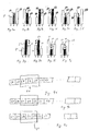
- each drawing illustrates a group of three neighboring pixels in the image signal.
- the pixels are illustrated as bars, which bars correspond to the luminance value for the given pixel.
- the pixel B 52 has a luminance value greater than that of the pixel A 50
- the pixel C 54 has a luminance value greater than that of the pixel B.
- the pixels A, B and C correspond to three adjacent pixels in the CMOS array 6. Under normal circumstances, one would not expect abrupt discontinuities in the change in luminance values. For instance, as the image changes from dark to light, the pattern shown in Figure 3a, with the pixels having increasing values, would be expected.
- the pixel B 52 is darker than the pixel A 50 and the pixel C 54 is darker than the pixel B 52 - indicating a normal transition from light to dark.
- the luminance for the middle pixel B 52 falls in the range of values defined by the luminance for its neighboring pixels A 50 and C 54.
- the middle pixel B 52 has a luminance that is greater than the luminance of both of its neighbors 50 and 54, indicating a discontinuity in the luminance trend for the image. Note, however, that the pixel B 52 of Figure 3c deviates from its nearest neighbor pixel C 54 by an amount t.
- the value t indicates a threshold deviation between neighboring pixels that can be tolerated before the middle pixel will be considered as defective.
- the deviation from the nearest pixel value is equal to or less than t.
- the luminance value for the middle pixel B 52 does not fall within the range of values between the neighboring pixels A 50 and C 54, and also deviates from the value of the nearest pixel by more than the threshold amount t. Under the circumstances illustrated in Figures 3g through 3j, the pixel B 52 will be considered to be defective.
- a pixel data stream preferably consists of 10-bit luminance values for each pixel of the CMOS array 6, which stream is fed to the defective-pixel filter 34.
- the defective-pixel filter 34 applies a moving window 60 across the pixel data stream as it passes through the filter.
- the first three pixels 50, 52, 54 of the stream are analyzed, with the pixel 52 being the middle pixel B under consideration (as illustrated, pixel data is moving from right to left).
- the moving window 60 has shifted one pixel or, more accurately, the pixels moving through defective-pixel filter 34 have shifted by one pixel, and the pixels 52, 54, and 56 are then analyzed, with the pixel 54 being the middle pixel B under consideration.
- the moving window has again shifted by one pixel and the pixels 54, 56, and 58 are analyzed, with the pixel 56 being the middle pixel B under consideration.
- the luminance value for the defective pixel will be replaced with an interpolated luminance value based upon the values of the neighboring pixels A and C.
- the incoming pixel data is fed to a first in first out (FIFO) register comprising register cells 70, 72, 74, 76, and 78. While the preferred embodiment provides for the advantageous feature that defective pixels are identified and corrected for in real-time without the need for large memory storage, other embodiments might provide for a DRAM, SRAM or other type of memory in which the incoming pixel data is fed and stored. Note that five pixels are loaded into the FIFO registers even though only three pixels are analyzed at one time. This is because the defective-pixel filter 34 can be configured for both monochrome images and for color images.
- color image sensors interlace the pixel sensors on each row in a Bayer pattern, as is illustrated in Figure 6, which illustrates a portion of a color image sensor.
- red sensors 102, 104, 106 are interlaced with green sensors 103, 105, 107.
- green sensors 108, 110, 112 are interlaced with blue sensors 109, 111, and 113.
- blue sensors 109, 111, and 113 are interlaced with blue sensors 109, 111, and 113.
- every other pixel should be selected for analysis, for instance pixels 102, 104, and 106 would be analyzed to determine if the pixel 104 was defective.
- the pixel 105 would be compared to like pixels 103 and 107. Otherwise, if the (green) value for the pixel 103 was compared to the (red) values of pixels 102 and 104, it would be very likely to have abrupt discontinuities, even though the pixel 103 was functioning normally. For instance, for a portion of the image in which the image was primarily red, pixels 102 and 104 would be expected to have high luminance values and the pixel 103 would be expected to have very low luminance values.
- the pixel A is selected from the register 72, the pixel B is selected from the register 74 and the pixel C is selected from the register 76.
- the pixel A is selected from register 70, the pixel B is selected from the register 74, and the pixel C is selected from the register 78, in order to ensure that like pixels are being compared.
- a multiplexer 80 selects the pixel A from either the register 72 or from the register 70 depending on whether the device is in the monochrome or color mode, and feeds the pixel value to a comparator 82.
- the comparator 82 the value of the pixel A is compared to the value of the pixel B from the register 74. If the comparison indicates that the pixel A has a greater value than the pixel B, a valid logic signal (logical high) is asserted on a signal line 86, which is connected to one input of a two-input AND gate 88. The other input to the AND gate 88 is fed from the comparator 96 wherein the value for the pixel B is compared to the value for the pixel C.
- the pixel C is selected by a multiplexer 98 from either the register 78 or the register 76, depending upon whether the device is in the monochrome or color mode. If the pixel B is greater in value than the pixel C, then the comparator 96 will assert a valid signal on a signal line 120, which is fed to the second input of the AND gate 88. If both inputs to the AND gate 88 are high (indicating that A is greater than B and B is greater than C), the AND gate 88 will assert a valid signal (logical high) to a four-input OR gate 122. This condition corresponds to the situation illustrated graphically in Figure 3b, which is an acceptable situation indicating that the pixel B is valid.
- the logical OR gate 122 will assert a valid signal (logical high) to a multiplexer 124, which will in turn allow the value for the pixel B, from the register 74, to be output from the defective-pixel filter 34 for further processing.
- a logical high signal will be treated as indicating a valid signal, although in other embodiments, a logical low signal could be used for a valid logic signal.
- the difference in the values of the pixel A and the pixel B is calculated in a block 90 and the difference is compared to the threshold t in a comparator 92.
- the value for the threshold t can be selected by a user and stored in a register 94. Alternatively, or if no value for t is selected by the user, a default value for t can be stored in the register 94.
- the threshold value can be automatically generated based upon an iterative process in which a feedback signal indicative of image quality is compared to a varying value for t until a threshold value is reached that effectively cancels out defective pixels without canceling out desired luminance variations that occur naturally in the image.
- the comparator 92 will output a logical high to the OR gate 122, which will also cause the multiplexer 124 to allow the pixel B to be passed.
- the fourth input of the OR gate 122 is fed from an AND gate 130.
- the first input to the AND gate 130 is the inverted output of the comparator 82 (via an inverter 132) and the second input is the inverted output of the comparator 96 (via an inverter 134).
- the AND gate 130 will output a valid signal (logical high) to the OR gate 122 when the pixel C is greater in value than the pixel B and the pixel B is greater in value than the pixel A. This corresponds to Figure 3a.
- the inputs to the OR gate 122 will be logical lows, and hence the control input to the multiplexer 124 will be a logical low.
- the multiplexer 124 will pass a corrected pixel B value to the output.
- This corrected pixel value is calculated in a block 136.
- More complex interpolations could be employed to generate the value for B corrected , such as using the values of the nearest two or three neighbors on either side of B, but such interpolations would require additional storage elements in which the neighboring pixel values are stored and would also require additional combinational logic (with its associated costs and real estate requirements).
- the circuit of Figure 5 is realized in combinational logic on a semiconductor chip using CMOS fabrication processes.
- the preferred embodiment filter is fabricated on the same chip as the sensor array, as provided for with a CMOS sensor array. While other types of arrays such as CCD array may also be used, they may not be as desirable for reasons of processing differences.
- the function could be achieved by a microprocessor running a sequence of program instructions.
- the circuitry could be realized in programmable gate array logic or other programmable logic.
- the preferred embodiments provide several advantageous features including the ability to eliminate temperature and time dependent pixel defects and the ability to filter both white pixels and dark pixels with adjustable thresholds.
- the adjustable threshold feature allows compensation for image spatial frequency and for degree of array pixel defects.
- the preferred embodiments operate at high speed in real time and do not require a frame or line memory to store an entire frame or line of data.
- Both the logic and the sensor array can be formed on a single chip and are compatible with CMOS operations.
- the method can be employed as a part of a wafer probe operation in order to determine wafer yield and is operable in either color or monochrome image modes.
- the described embodiments maintain high frequency edge components, such as a rapid transition from a dark to very bright object, or from a bright to dark object.
Landscapes
- Engineering & Computer Science (AREA)
- Multimedia (AREA)
- Signal Processing (AREA)
- Transforming Light Signals Into Electric Signals (AREA)
- Solid State Image Pick-Up Elements (AREA)
- Picture Signal Circuits (AREA)
- Analogue/Digital Conversion (AREA)
- Color Television Image Signal Generators (AREA)
- Image Input (AREA)
Abstract
Description
Claims (30)
- A filter for filtering an image which includes a plurality of picture elements each represented by a luminance or a chrominance value, including:means for selecting a picture element and its two adjacent picture elements,means for determining whether the selected picture element lies between the two adjacent picture elements in value,means for determining whether the selected picture element differs in value from both of the two adjacent picture elements by more than a set amount andmeans for replacing the selected picture element, in value, by a value dependent on the two adjacent picture elements, when, in value, the selected picture element does not lie between the two adjacent picture elements and differs from both of the two adjacent picture elements by more than the set amount andmeans for repeating the procedure for further picture elements serving as the selected picture element.
- A filter as claimed in claim 1, including means for replacing the selected picture element, in value, by an average of the values of the two adjacent picture elements.
- A filter as claimed in claim 1, including means for replacing the selected picture element, in value, by an interpolation dependent on the values of the two adjacent picture elements.
- A filter as claimed in any one of claims 1 to 3 comprising: a first comparator circuit for receiving as input a first picture element value and a second picture element value and outputting a valid logic signal to a first input of an AND circuit and to a first inverter when the first picture element value is greater than the second picture element value,a first difference calculator for receiving as input said first picture element value and said second picture element value and outputting to a first input of a second comparator circuit a first difference value corresponding to the difference between said first and second picture element values;said second comparator circuit also for receiving as input a threshold value and outputting a valid logic signal to a first input of an OR circuit when the first difference value is less than or equal to the set amount;a third comparator circuit for receiving as input said second picture element value and a third picture element value and outputting a valid logic signal to a second input of said first AND circuit and to a second inverter when the second picture element value is greater than the third picture element value and
a second difference calculator for receiving as input said second picture element value and said third picture element value and outputting a second difference value corresponding to the difference between said second and third picture element values to a first input of a fourth comparator circuit,said fourth comparator circuit also for receiving as input the set amount threshold value and outputting a valid logic signal to a third input of said OR circuit when the second difference value is less than or equal to the set amount anda second AND circuit coupled to said first and second inverters and having an output coupled to a fourth input of said OR circuit. - A filter as claimed in claim 4 further comprising:a corrected picture element calculation block for receiving as input said first and third picture element values and outputting a corrected picture element value,a multiplexer having a first input coupled to the output of said corrected picture element calculation block and receiving as a second input said picture element value and having a control input coupled to an output of said OR circuit.
- A filter as claimed in any one of claims 1 to 5, further comprising registers for storing picture element values.
- A filter as claimed in any one of claims 4 to 6, capable of operating in both monochrome and color mode and further comprising:at least one multiplexer for receiving as input the picture element values stored in at least two registers and outputting one of said picture element values in response to an indication of monochrome or color mode operation.
- A filter as claimed in any one of claims 4 to 7, wherein said first, second, and third picture element values are ten bit digital values.
- A filter as claimed in any one of claims 1 to 8, further comprising a threshold value register for storing the said set amount.
- A filter as claimed in claim 9, including means permitting a user to enter the set amount in the threshold value register.
- A filter as claimed in claim 9, including means for providing the set amount from a feedback signal indicative of image quality.
- A filter as claimed in any one of claims 4 to 8, wherein said comparator circuits, difference calculators, and registers are fabricated with CMOS processes.
- A filter as claimed in any one of claims 1 to 12, including a general purpose microprocessor.
- A digital imaging device including a filter as claimed in any one of claims 1 to 13 comprising:a substrate,a sensor array formed on the substrate, the array generating an electrical signal corresponding to the amount of light impinging upon the array andimaging logic formed on the substrate, coupled to the sensor array and receiving the electrical signal, the imaging logic including an analog to digital converter receiving the electrical signal and outputting digital picture element values.
- A digital imaging device as claimed in claim 14, further comprising a first in first out register wherein said picture element values are stored.
- A digital imaging device as claimed in claim 14 or claim 15, wherein the filter operates in real time.
- A digital imaging device as claimed in any one of claim 14 to 16, wherein the sensor array is comprised of CMOS cells.
- A digital imager including a filter as claimed in any one of claims 1 to 13 comprising:a lens mechanism,a sensor array positioned within a focal plane of said lens mechanism,an analog buffer and amplifier coupled to an output of said sensor array andimaging logic coupled to said amplifier, the filter being included in the said imaging logic.
- A digital imager as claimed in claim 18, wherein said sensor array and said imaging logic are fabricated on a single integrated circuit.
- A digital imager as claimed in claim 18 or 19, wherein the sensor array is comprised of CMOS cells.
- A digital imager as claimed in claim 18 or 19, wherein the sensor array is comprised of CCD cells.
- A digital imager as claimed in any one of claims 18 to 21, wherein the imaging logic includes combinational logic.
- A digital imager as claimed in any one of claims 18 to 22, wherein the imaging logic includes a microprocessor.
- A method of filtering an image including a plurality of picture elements each represented by a luminance or a chrominance value, including the steps of:selecting a picture element and its two adjacent picture elements,determining whether the selected picture element lies, in value, between the two adjacent picture elements,determining whether the selected picture element differs, in value, from both of the two adjacent picture elements by more than a set amount andwhen the selected picture element does not lie, in value, between the two adjacent picture elements and differs from both of the two adjacent picture elements by more than the set amount,replacing the selected picture element, in value, by a value dependent on the two adjacent picture elements,the procedure being repeated for further picture elements serving as the selected picture element.
- A method as claimed in claim 24 comprising:determining a first difference value between the luminance value of the selected picture element and the luminance value of a first neighboring picture element,comparing the first difference value to the set value,determining a second difference value between the luminance of the selected picture element and the luminance value of a second neighboring picture element,comparing the second difference value to the set value,detecting whether the luminance value for the selected picture element falls within an acceptable range defined by the luminance value for the first neighboring picture element and the luminance value for the second neighboring picture element andidentifying the selected picture element as defective if the luminance value for the selected picture element does not fall within the acceptable range and neither the first difference value nor the second difference value is less than or equal to the set value.
- The method as claimed in claim 24 or claim 25, wherein an average of the luminance value of the first neighboring picture element and the luminance value of the second neighboring picture element replaces the selected picture element in value.
- A method as claimed in claim 24 or claim 25, wherein an interpolated value taking account of two or more neighboring picture elements on either side of the selected picture element replaces the selected picture element in value.
- A method as claimed in any one of claims 24 to 27, wherein the set value is entered in a register by a user.
- A method as claimed in any one of claims 24 to 27, wherein the set value is determined from a feedback signal indicative of image quality.
- A method as claimed in any one of claims 24 to 29, performed in real time.
Applications Claiming Priority (6)
| Application Number | Priority Date | Filing Date | Title |
|---|---|---|---|
| US12440899P | 1999-03-15 | 1999-03-15 | |
| US12453899P | 1999-03-15 | 1999-03-15 | |
| US124538P | 1999-03-15 | ||
| US124408P | 1999-03-15 | ||
| US47565299A | 1999-12-30 | 1999-12-30 | |
| US475652 | 1999-12-30 |
Publications (3)
| Publication Number | Publication Date |
|---|---|
| EP1045578A2 true EP1045578A2 (en) | 2000-10-18 |
| EP1045578A3 EP1045578A3 (en) | 2000-11-08 |
| EP1045578B1 EP1045578B1 (en) | 2003-08-20 |
Family
ID=27383103
Family Applications (2)
| Application Number | Title | Priority Date | Filing Date |
|---|---|---|---|
| EP00302086A Withdrawn EP1067775A3 (en) | 1999-03-15 | 2000-03-15 | Digital imaging control with selective intensity resolution enhancement |
| EP00302082A Expired - Lifetime EP1045578B1 (en) | 1999-03-15 | 2000-03-15 | Filtering of defective picture elements in digital imagers |
Family Applications Before (1)
| Application Number | Title | Priority Date | Filing Date |
|---|---|---|---|
| EP00302086A Withdrawn EP1067775A3 (en) | 1999-03-15 | 2000-03-15 | Digital imaging control with selective intensity resolution enhancement |
Country Status (3)
| Country | Link |
|---|---|
| EP (2) | EP1067775A3 (en) |
| AT (1) | ATE247885T1 (en) |
| DE (1) | DE60004595T2 (en) |
Cited By (10)
| Publication number | Priority date | Publication date | Assignee | Title |
|---|---|---|---|---|
| EP1248458A3 (en) * | 2001-04-06 | 2003-03-05 | Agilent Technologies, Inc. (a Delaware corporation) | System and method for correcting erroneous image signals from defective photosensitive pixels during analog-to-digital conversion |
| EP1271933A3 (en) * | 2001-06-28 | 2003-05-28 | Agilent Technologies, Inc. (a Delaware corporation) | Bad pixel detection and correction in an image sensing device |
| DE10209552A1 (en) * | 2002-03-04 | 2003-10-02 | Plettac Ag | Method and device for compensating defective pixels of a CCD sensor |
| EP1418751A1 (en) * | 2002-10-28 | 2004-05-12 | Samsung Electronics Co., Ltd. | CCD camera with defective cell compensation |
| DE10255021A1 (en) * | 2002-11-25 | 2004-06-17 | Zeiss Optronik Gmbh | Method and device for generating homogenized image data in scanning imaging devices |
| WO2005011261A1 (en) * | 2003-07-07 | 2005-02-03 | Zoran Corporation | Dynamic identification and correction of defective pixels |
| EP1594308A1 (en) * | 2004-05-07 | 2005-11-09 | Dialog Semiconductor GmbH | Single line Bayer filter RGB bad pixel correction |
| US7433512B2 (en) | 2004-11-09 | 2008-10-07 | Dalsa Corporation | Method and apparatus for finding and correcting single-pixel noise defects in a two-dimensional camera pixel field and a camera provided with such an apparatus |
| TWI505702B (en) * | 2008-10-03 | 2015-10-21 | 慧榮科技股份有限公司 | Photographic device and image sensor dead point compensation method |
| DE102006040349B4 (en) * | 2006-08-29 | 2016-11-10 | Robert Bosch Gmbh | Method and device for detecting defective pixels of an image sensor in a driver assistance system |
Families Citing this family (4)
| Publication number | Priority date | Publication date | Assignee | Title |
|---|---|---|---|---|
| US6686957B1 (en) * | 1999-03-31 | 2004-02-03 | Cirrus Logic, Inc. | Preview mode low resolution output system and method |
| US8081837B2 (en) * | 2006-02-07 | 2011-12-20 | Intel Corporation | Image sensor array leakage and dark current compensation |
| CN101344917B (en) * | 2007-07-13 | 2012-05-02 | 晨星半导体股份有限公司 | Fingerprint detection circuit |
| TWI705381B (en) * | 2019-02-23 | 2020-09-21 | 友達光電股份有限公司 | Finger print sensing apparatus |
Family Cites Families (9)
| Publication number | Priority date | Publication date | Assignee | Title |
|---|---|---|---|---|
| US4541116A (en) * | 1984-02-27 | 1985-09-10 | Environmental Research Institute Of Mi | Neighborhood image processing stage for implementing filtering operations |
| GB8524880D0 (en) * | 1985-10-09 | 1985-11-13 | British Telecomm | Video level control |
| GB8614212D0 (en) * | 1986-06-11 | 1986-07-16 | Kodak Ltd | Image processing method |
| KR100188897B1 (en) * | 1990-01-31 | 1999-06-01 | 이데이 노부유끼 | An image defect correcting circuit for a solid state imager |
| EP0496573B1 (en) * | 1991-01-24 | 1995-12-20 | Matsushita Electric Industrial Co., Ltd. | Pixel defect removing circuit for solid-state image pickup device |
| US5392070A (en) * | 1991-11-26 | 1995-02-21 | Kabushiki Kaisha Toshiba | Apparatus for correcting faulty pixel signals by replacing the faulty pixel signals with normal pixel signals |
| US5790061A (en) * | 1995-02-24 | 1998-08-04 | Nec Corporation | Adaptive A/D converting device for adaptively converting and input analog signal into an output digital signal having a constant quantizing error |
| JP3428287B2 (en) * | 1996-04-12 | 2003-07-22 | ソニー株式会社 | Clamp circuit and imaging device using the same |
| US5841385A (en) * | 1996-09-12 | 1998-11-24 | Advanced Micro Devices, Inc. | System and method for performing combined digital/analog automatic gain control for improved clipping suppression |
-
2000
- 2000-03-15 EP EP00302086A patent/EP1067775A3/en not_active Withdrawn
- 2000-03-15 DE DE60004595T patent/DE60004595T2/en not_active Expired - Lifetime
- 2000-03-15 AT AT00302082T patent/ATE247885T1/en not_active IP Right Cessation
- 2000-03-15 EP EP00302082A patent/EP1045578B1/en not_active Expired - Lifetime
Cited By (15)
| Publication number | Priority date | Publication date | Assignee | Title |
|---|---|---|---|---|
| EP1248458A3 (en) * | 2001-04-06 | 2003-03-05 | Agilent Technologies, Inc. (a Delaware corporation) | System and method for correcting erroneous image signals from defective photosensitive pixels during analog-to-digital conversion |
| EP1271933A3 (en) * | 2001-06-28 | 2003-05-28 | Agilent Technologies, Inc. (a Delaware corporation) | Bad pixel detection and correction in an image sensing device |
| US6737625B2 (en) | 2001-06-28 | 2004-05-18 | Agilent Technologies, Inc. | Bad pixel detection and correction in an image sensing device |
| DE10209552A1 (en) * | 2002-03-04 | 2003-10-02 | Plettac Ag | Method and device for compensating defective pixels of a CCD sensor |
| EP1418751A1 (en) * | 2002-10-28 | 2004-05-12 | Samsung Electronics Co., Ltd. | CCD camera with defective cell compensation |
| DE10255021B4 (en) * | 2002-11-25 | 2007-02-22 | Carl Zeiss Optronics Gmbh | Method and device for generating image data of a scene taking into account inhomogeneities in the signal sensitivities of sensor elements in scanning imaging devices |
| DE10255021A1 (en) * | 2002-11-25 | 2004-06-17 | Zeiss Optronik Gmbh | Method and device for generating homogenized image data in scanning imaging devices |
| WO2005011261A1 (en) * | 2003-07-07 | 2005-02-03 | Zoran Corporation | Dynamic identification and correction of defective pixels |
| US7388609B2 (en) | 2003-07-07 | 2008-06-17 | Zoran Corporation | Dynamic identification and correction of defective pixels |
| CN1981514B (en) * | 2003-07-07 | 2010-04-21 | 卓然公司 | A Method for Dynamically Identifying and Correcting Bad Pixels |
| US8098304B2 (en) | 2003-07-07 | 2012-01-17 | Zoran Corporation | Dynamic identification and correction of defective pixels |
| EP1594308A1 (en) * | 2004-05-07 | 2005-11-09 | Dialog Semiconductor GmbH | Single line Bayer filter RGB bad pixel correction |
| US7433512B2 (en) | 2004-11-09 | 2008-10-07 | Dalsa Corporation | Method and apparatus for finding and correcting single-pixel noise defects in a two-dimensional camera pixel field and a camera provided with such an apparatus |
| DE102006040349B4 (en) * | 2006-08-29 | 2016-11-10 | Robert Bosch Gmbh | Method and device for detecting defective pixels of an image sensor in a driver assistance system |
| TWI505702B (en) * | 2008-10-03 | 2015-10-21 | 慧榮科技股份有限公司 | Photographic device and image sensor dead point compensation method |
Also Published As
| Publication number | Publication date |
|---|---|
| DE60004595T2 (en) | 2004-03-18 |
| DE60004595D1 (en) | 2003-09-25 |
| ATE247885T1 (en) | 2003-09-15 |
| EP1067775A2 (en) | 2001-01-10 |
| EP1067775A3 (en) | 2002-08-07 |
| EP1045578A3 (en) | 2000-11-08 |
| EP1045578B1 (en) | 2003-08-20 |
Similar Documents
| Publication | Publication Date | Title |
|---|---|---|
| US7286179B2 (en) | Defective pixel filtering for digital imagers | |
| US7133073B1 (en) | Method and apparatus for color interpolation | |
| US6965395B1 (en) | Methods and systems for detecting defective imaging pixels and pixel values | |
| US8310577B1 (en) | Method and apparatus for color compensation | |
| US6888568B1 (en) | Method and apparatus for controlling pixel sensor elements | |
| US8571346B2 (en) | Methods and devices for defective pixel detection | |
| EP1045578B1 (en) | Filtering of defective picture elements in digital imagers | |
| US7924330B2 (en) | Methods and apparatuses for double sided dark reference pixel row-wise dark level non-uniformity compensation in image signals | |
| US8442345B2 (en) | Method and apparatus for image noise reduction using noise models | |
| US7283164B2 (en) | Method for detecting and correcting defective pixels in a digital image sensor | |
| KR101001431B1 (en) | Pixel defect detection correction device and pixel defect detection correction method | |
| WO2003103275A1 (en) | Method and apparatus for real time identification and correction of pixel defects for image sensor arrays | |
| JPH11252464A (en) | Pixel correction system and method for CMOS imagers | |
| US7106912B2 (en) | Circuit for correction of white pixel defects and an image sensor using the circuit for correction of white pixel defects | |
| JP3544304B2 (en) | Pixel defect correction device and pixel defect correction method | |
| US7304673B2 (en) | Image sensor array with substitutional circuit distribution | |
| JP5262953B2 (en) | Image processing apparatus, image processing method, and program | |
| JP3257131B2 (en) | Automatic defect detection device for solid-state imaging device and solid-state imaging device | |
| JP2004023683A (en) | Defect correction apparatus and method for solid-state imaging device | |
| JP4166974B2 (en) | Pixel scratch detection / correction device | |
| US20090091642A1 (en) | Image defect correction system using directional detection | |
| JP4178919B2 (en) | Noise removal method, imaging apparatus, and noise removal program | |
| WO2001013649A1 (en) | Method and apparatus for color interpolation | |
| CN101335827B (en) | Image defect correcting system using oriented detection method | |
| JP3361077B2 (en) | Solid-state imaging device |
Legal Events
| Date | Code | Title | Description |
|---|---|---|---|
| PUAI | Public reference made under article 153(3) epc to a published international application that has entered the european phase |
Free format text: ORIGINAL CODE: 0009012 |
|
| PUAL | Search report despatched |
Free format text: ORIGINAL CODE: 0009013 |
|
| AK | Designated contracting states |
Kind code of ref document: A2 Designated state(s): AT BE CH CY DE DK ES FI FR GB GR IE IT LI LU MC NL PT SE |
|
| AX | Request for extension of the european patent |
Free format text: AL;LT;LV;MK;RO;SI |
|
| AK | Designated contracting states |
Kind code of ref document: A3 Designated state(s): AT BE CH CY DE DK ES FI FR GB GR IE IT LI LU MC NL PT SE |
|
| AX | Request for extension of the european patent |
Free format text: AL;LT;LV;MK;RO;SI |
|
| 17P | Request for examination filed |
Effective date: 20010427 |
|
| AKX | Designation fees paid |
Free format text: DE FR GB IT NL |
|
| RBV | Designated contracting states (corrected) |
Designated state(s): AT BE CH CY DE DK ES FI FR GB GR IE IT LI LU MC NL PT SE |
|
| 17Q | First examination report despatched |
Effective date: 20010629 |
|
| RBV | Designated contracting states (corrected) |
Designated state(s): DE FR GB IT NL |
|
| RBV | Designated contracting states (corrected) |
Designated state(s): AT BE CH CY DE DK ES FI FR GB GR IE IT LI LU MC NL PT SE |
|
| GRAH | Despatch of communication of intention to grant a patent |
Free format text: ORIGINAL CODE: EPIDOS IGRA |
|
| GRAH | Despatch of communication of intention to grant a patent |
Free format text: ORIGINAL CODE: EPIDOS IGRA |
|
| GRAA | (expected) grant |
Free format text: ORIGINAL CODE: 0009210 |
|
| AK | Designated contracting states |
Designated state(s): AT BE CH CY DE DK ES FI FR GB GR IE IT LI LU MC NL PT SE |
|
| PG25 | Lapsed in a contracting state [announced via postgrant information from national office to epo] |
Ref country code: AT Free format text: LAPSE BECAUSE OF FAILURE TO SUBMIT A TRANSLATION OF THE DESCRIPTION OR TO PAY THE FEE WITHIN THE PRESCRIBED TIME-LIMIT Effective date: 20030820 Ref country code: LI Free format text: LAPSE BECAUSE OF FAILURE TO SUBMIT A TRANSLATION OF THE DESCRIPTION OR TO PAY THE FEE WITHIN THE PRESCRIBED TIME-LIMIT Effective date: 20030820 Ref country code: FI Free format text: LAPSE BECAUSE OF FAILURE TO SUBMIT A TRANSLATION OF THE DESCRIPTION OR TO PAY THE FEE WITHIN THE PRESCRIBED TIME-LIMIT Effective date: 20030820 Ref country code: BE Free format text: LAPSE BECAUSE OF FAILURE TO SUBMIT A TRANSLATION OF THE DESCRIPTION OR TO PAY THE FEE WITHIN THE PRESCRIBED TIME-LIMIT Effective date: 20030820 Ref country code: CH Free format text: LAPSE BECAUSE OF FAILURE TO SUBMIT A TRANSLATION OF THE DESCRIPTION OR TO PAY THE FEE WITHIN THE PRESCRIBED TIME-LIMIT Effective date: 20030820 Ref country code: NL Free format text: LAPSE BECAUSE OF FAILURE TO SUBMIT A TRANSLATION OF THE DESCRIPTION OR TO PAY THE FEE WITHIN THE PRESCRIBED TIME-LIMIT Effective date: 20030820 Ref country code: CY Free format text: LAPSE BECAUSE OF FAILURE TO SUBMIT A TRANSLATION OF THE DESCRIPTION OR TO PAY THE FEE WITHIN THE PRESCRIBED TIME-LIMIT Effective date: 20030820 Ref country code: IT Free format text: LAPSE BECAUSE OF FAILURE TO SUBMIT A TRANSLATION OF THE DESCRIPTION OR TO PAY THE FEE WITHIN THE PRESCRIBED TIME-LIMIT;WARNING: LAPSES OF ITALIAN PATENTS WITH EFFECTIVE DATE BEFORE 2007 MAY HAVE OCCURRED AT ANY TIME BEFORE 2007. THE CORRECT EFFECTIVE DATE MAY BE DIFFERENT FROM THE ONE RECORDED. Effective date: 20030820 |
|
| REG | Reference to a national code |
Ref country code: GB Ref legal event code: FG4D |
|
| REG | Reference to a national code |
Ref country code: CH Ref legal event code: EP |
|
| REG | Reference to a national code |
Ref country code: IE Ref legal event code: FG4D |
|
| REF | Corresponds to: |
Ref document number: 60004595 Country of ref document: DE Date of ref document: 20030925 Kind code of ref document: P |
|
| PG25 | Lapsed in a contracting state [announced via postgrant information from national office to epo] |
Ref country code: SE Free format text: LAPSE BECAUSE OF FAILURE TO SUBMIT A TRANSLATION OF THE DESCRIPTION OR TO PAY THE FEE WITHIN THE PRESCRIBED TIME-LIMIT Effective date: 20031120 Ref country code: DK Free format text: LAPSE BECAUSE OF FAILURE TO SUBMIT A TRANSLATION OF THE DESCRIPTION OR TO PAY THE FEE WITHIN THE PRESCRIBED TIME-LIMIT Effective date: 20031120 Ref country code: GR Free format text: LAPSE BECAUSE OF FAILURE TO SUBMIT A TRANSLATION OF THE DESCRIPTION OR TO PAY THE FEE WITHIN THE PRESCRIBED TIME-LIMIT Effective date: 20031120 |
|
| PG25 | Lapsed in a contracting state [announced via postgrant information from national office to epo] |
Ref country code: ES Free format text: LAPSE BECAUSE OF FAILURE TO SUBMIT A TRANSLATION OF THE DESCRIPTION OR TO PAY THE FEE WITHIN THE PRESCRIBED TIME-LIMIT Effective date: 20031201 |
|
| PG25 | Lapsed in a contracting state [announced via postgrant information from national office to epo] |
Ref country code: PT Free format text: LAPSE BECAUSE OF FAILURE TO SUBMIT A TRANSLATION OF THE DESCRIPTION OR TO PAY THE FEE WITHIN THE PRESCRIBED TIME-LIMIT Effective date: 20040120 |
|
| NLV1 | Nl: lapsed or annulled due to failure to fulfill the requirements of art. 29p and 29m of the patents act | ||
| REG | Reference to a national code |
Ref country code: CH Ref legal event code: PL |
|
| PG25 | Lapsed in a contracting state [announced via postgrant information from national office to epo] |
Ref country code: LU Free format text: LAPSE BECAUSE OF NON-PAYMENT OF DUE FEES Effective date: 20040315 Ref country code: IE Free format text: LAPSE BECAUSE OF NON-PAYMENT OF DUE FEES Effective date: 20040315 |
|
| PG25 | Lapsed in a contracting state [announced via postgrant information from national office to epo] |
Ref country code: MC Free format text: LAPSE BECAUSE OF NON-PAYMENT OF DUE FEES Effective date: 20040331 |
|
| ET | Fr: translation filed | ||
| PLBE | No opposition filed within time limit |
Free format text: ORIGINAL CODE: 0009261 |
|
| STAA | Information on the status of an ep patent application or granted ep patent |
Free format text: STATUS: NO OPPOSITION FILED WITHIN TIME LIMIT |
|
| 26N | No opposition filed |
Effective date: 20040524 |
|
| REG | Reference to a national code |
Ref country code: IE Ref legal event code: MM4A |
|
| REG | Reference to a national code |
Ref country code: FR Ref legal event code: PLFP Year of fee payment: 16 |
|
| PGFP | Annual fee paid to national office [announced via postgrant information from national office to epo] |
Ref country code: GB Payment date: 20150224 Year of fee payment: 16 Ref country code: FR Payment date: 20150224 Year of fee payment: 16 |
|
| PGFP | Annual fee paid to national office [announced via postgrant information from national office to epo] |
Ref country code: DE Payment date: 20150331 Year of fee payment: 16 |
|
| REG | Reference to a national code |
Ref country code: DE Ref legal event code: R119 Ref document number: 60004595 Country of ref document: DE |
|
| GBPC | Gb: european patent ceased through non-payment of renewal fee |
Effective date: 20160315 |
|
| REG | Reference to a national code |
Ref country code: FR Ref legal event code: ST Effective date: 20161130 |
|
| PG25 | Lapsed in a contracting state [announced via postgrant information from national office to epo] |
Ref country code: FR Free format text: LAPSE BECAUSE OF NON-PAYMENT OF DUE FEES Effective date: 20160331 Ref country code: GB Free format text: LAPSE BECAUSE OF NON-PAYMENT OF DUE FEES Effective date: 20160315 Ref country code: DE Free format text: LAPSE BECAUSE OF NON-PAYMENT OF DUE FEES Effective date: 20161001 |