EP1043868A2 - Optoelectronic network interface device - Google Patents
Optoelectronic network interface device Download PDFInfo
- Publication number
- EP1043868A2 EP1043868A2 EP00302539A EP00302539A EP1043868A2 EP 1043868 A2 EP1043868 A2 EP 1043868A2 EP 00302539 A EP00302539 A EP 00302539A EP 00302539 A EP00302539 A EP 00302539A EP 1043868 A2 EP1043868 A2 EP 1043868A2
- Authority
- EP
- European Patent Office
- Prior art keywords
- interface device
- network
- ports
- optical
- electronic circuits
- Prior art date
- Legal status (The legal status is an assumption and is not a legal conclusion. Google has not performed a legal analysis and makes no representation as to the accuracy of the status listed.)
- Withdrawn
Links
Images


Classifications
-
- H—ELECTRICITY
- H04—ELECTRIC COMMUNICATION TECHNIQUE
- H04Q—SELECTING
- H04Q11/00—Selecting arrangements for multiplex systems
- H04Q11/0001—Selecting arrangements for multiplex systems using optical switching
- H04Q11/0003—Details
-
- H—ELECTRICITY
- H04—ELECTRIC COMMUNICATION TECHNIQUE
- H04Q—SELECTING
- H04Q11/00—Selecting arrangements for multiplex systems
- H04Q11/0001—Selecting arrangements for multiplex systems using optical switching
- H04Q11/0062—Network aspects
- H04Q11/0067—Provisions for optical access or distribution networks, e.g. Gigabit Ethernet Passive Optical Network (GE-PON), ATM-based Passive Optical Network (A-PON), PON-Ring
-
- H—ELECTRICITY
- H04—ELECTRIC COMMUNICATION TECHNIQUE
- H04Q—SELECTING
- H04Q11/00—Selecting arrangements for multiplex systems
- H04Q11/0001—Selecting arrangements for multiplex systems using optical switching
- H04Q11/0062—Network aspects
- H04Q11/0071—Provisions for the electrical-optical layer interface
Definitions
- This invention relates to a network interface device and, more particularly, to a dynamically reconfigurable optoelectronic network interface device.
- LAN Local Area Network
- the capability of reconfiguring the ports of a network interface device is essential for accommodating the changing needs of end-users. Specifically, this necessitates dynamic reconfigurability of the ports of a network interface device while the device is in operation within the communication network.
- a typical LAN interface device has multiple ports that are designed for use with different data rates corresponding to the data rates used in the communication network.
- the interface device may have a large number of 100 Megabits/s ports and several 1 Gigabit/s ports.
- the interface device ports are configured according to the initial requirements, such as bandwidth needs, of end-users in the network. Although, reconfiguration of the end-user interface ports in such a communication network is possible, it none-the-less presents several significant limitations.
- reconfiguration of the interface ports When used in a communication network that is operational, reconfiguration of the interface ports must be performed on the network side (e.g. in the communication network infrastructure) of the LAN interface device connection. This is usually accomplished by placing several manually reconfigurable optical patch panels with jumper fibers or an expensive optical switch in the wiring infrastructure. Subsequently, port and network modifications can be made by appropriate changes in the optical patch panels or optical switch. Since these methods of reconfiguration are generally costly and/or time consuming, they are prohibitive to the dynamic reconfiguration of network interface ports in response to the changing communication needs of end-users. Thus, opportunity exists to employ a more effective and less costly means to achieve reconfigurability in communication networks.
- rapid port reconfigurability is achieved in a communication network by utilizing an optoelectronic interface device with an integrated electronic switch between the ports and the remaining electronic circuits.
- the interface device's port connections to the network can be dynamically altered without disturbing physical connections to end-users.
- dynamic port reconfiguration is enabled with a controllable electronic switch integrated into the optoelectronic interface device. Consequently, additional and costly optical switching elements to provide port reconfigurability are not required in the communication network.
- the present invention's network interface device provides dynamic reconfiguration of ports while supporting different signal bandwidths or data-rates at each of the ports.
- the network interface device supplies a means for dynamically allocating bandwidth according to an end-users changing needs.
- the optoelectronic interface device with an electronic switch is integrated onto a single optoelectronic Very Large Scale Integration (VLSI) chip. Therefore, a reduction in the cost of manufacturing is expected through the miniaturization and integration of a number of formerly discrete circuits.
- VLSI Very Large Scale Integration
- the present invention is an optoelectmnic network interface device having a controllable electronic switch that is well suited for such a reconfiguration application.
- the interface device is designed for use with multiple input fibers in a communication network in which each input fiber can support different data rates.
- the controllable electronic switch allows the interface device to provide a dynamic allocation of ports, while supporting different data rates at each of the ports.
- the invention is not limited to use with any particular type of communication network.
- the integrated optoelectronic network interface device delivers the advantages of a multi-port conventional LAN interface with an electronic switch, while overcoming certain disadvantages of prior network interfaces.
- the term "integrated" shall mean that the components recited are either integrated in a single monolithic chip or combined as a plurality of chips that are coupled together on a single circuit board.
- the interface device is an integrated structure including at least one port, also known as an optoelectronic transceiver, to receive and send optical signals from and to input fibers.
- the ports also convert (1) optical signals to electrical signals and (2) electrical signals to optical signals.
- the ports are coupled to a controllable electronic switch for routing electrical signals.
- the electronic switch is coupled to a plurality of electronic circuits, for example, interface and logic circuits to receive and send electrical signals between the electronic switch and the corresponding end-users.
- Port reconfiguration is accomplished by using the electronic switch to route the electronic signals to the appropriate electronic circuits and ultimately to the end-users.
- the connection path between each port and the electronic circuits are established.
- the ports of the interface device are dynamically reconfigured with each cross-connect of the electronic switch.
- FIG. 1 shows one exemplary embodiment of the interface device, specifically, optoelectronic interface 100 includes interface ports 106.
- Each interface port 106 includes a laser/detector pair 102 coupled to Driver/receiver 104.
- the combination of laser/detector 102 and driver/receiver 104 is commonly known as an optoelectronic transceiver.
- the optoelectronic transceivers process optical signals and, in particular, transmit and receive signals to and from multiple input fiber pairs 108.
- the optoelectronic transceivers convert (1) optical signals to electrical signals and (2) electrical signals to optical signals.
- the signal data rates can differ, for example, 10 Megabits/s, 100 Megabits/s, and 1 Gigabit/s.
- each input fiber-pair 108 is associated with a particular port 106, both ports 106 and fiber-pairs 108 are designed for use with multiple data rates, therefore, the ports and fiber-pairs are not dedicated to a specific data rate.
- Electronic circuits 112 are also integrated into interface device 100.
- Electronic circuits 112 may include specific data-rate interface electronics as well as associated physical layer circuits, such as encoders/decoders, serializers-deserializers and Media-Access Control (MAC) layer circuits.
- specific physical layer circuits may correspond to various bit rates, such as 10Megabits/s, 100Megabits/s, and 1 Gigabit/s.
- specific physical layer circuits may also be associated with various protocols, such as Ethernet, Fiber-channel, FDDI, ATM, and the like.
- an electronic switch 110 Coupled to drivers/receivers 104 and electronic circuits 112 is an electronic switch 110.
- Conventional electronic switches are also known in the art as a digital crossbar interconnection or electronic cross-connect. Such switches may be implemented, for example, by electronic circuitry and may incorporate such functionality as in the commercially available Lucent Technologies Digital Access Cross-Connect Switch (DACS) family of switches.
- DAS Digital Access Cross-Connect Switch
- electronic switch 110 is integrated into interface device 100, thereby forming this new combination.
- Electronic switch 110 is coupled to electronic circuits 112, such that each electronic signal received from drivers/receivers 104 can be routed to any of the electronic circuits 112. Similarly, each electronic signal transmitted from the electronic circuits 112 can be routed to any of the drivers/receivers 104 through switch 110.
- a control signal is generated on lead 114, which is coupled to electronic switch 110 for the purpose of selecting the desired connection paths or routing positions in electronic switch 110 between ports 106 and electronic circuits 112.
- the control signal may be generated by any conventional control device or method including, but not limited to: 1) local control, such as a LAN administrator; 2) remote control, such as a network control center; or 3) automated through the use of dynamic network reconfiguration software. In this manner, a connection can be dynamically formed from any port 106 to any electronic circuit 112 by the electronic switch.
- input fiber pairs 108 may comprise individual fibers or may be bundled in a fiber-ribbon.
- the use of a fiber-ribbon will decrease the required footprint of the fibers, as well as offer cost reduction and ease of assembly.
- fiber-ribbons are not as easily moved or reconfigured as individual fibers and, therefore, are less desirable in traditional LAN interface applications, the present invention's electronic reconfigurability, via the switch, overcomes this limitation.
- a conventional feedback mechanism (not shown) can be incorporated into the optoelectronic interface 100 of FIG. 1 to optimize the optical transceivers according to various data rates received from fiber-pairs 108.
- the optical transceiver optimization consists of adapting the bandwidth of the drivers/receivers 104 to correspond to the incoming optical signals from input fibers 108.
- the first stage of the detector and receiver typically known as pre-amplifiers, have a bandwidth range that covers all of the bit-rates of the optical signals received from fiber-pairs 108, for example, 0.0 Hz through 1.25 GHz.
- network interface device 100 is configured to provide port connections to end-users, in which port one is connected to end-user and port two is connected to end-user two and so on.
- This port configuration may correspond to the initial needs of the end-users at the time the communication network was installed.
- port one may have a data rate of 10 Megabit/s
- port two may have a data rate of 100 Megabits/s
- port N may have a data rate of 1 Gigabit/s.
- the ports can be reconfigured by simply sending a control signal to electronic switch 110 to make the appropriate connections in interface device 100, thus, providing each end-user with a port connection corresponding to the new requirements.
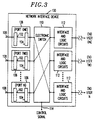
- end-user one can receive a greater bandwidth allocation by having electronic switch 110 form a cross-connect path from end-user one to port two, as shown in FIG 3, thus providing end-user one with a 100 Megabits/s port.
- the other ports in FIG 3 are reconfigured, via electronic switch 110, to provide other end-users with a suitable port coterminous with the end-users' needs.
- the interface device's ports are not only dynamically reconfigured but also reconfigured without physical rewiring or optical circuits as in the prior art.
- the optoelectronic interface can be integrated onto a single monolithic chip, to form an optoelectronic-VLSI (OE-VLSI) interface chip.
- OE-VLSI optoelectronic-VLSI
- Such an OE-VLSI interface chip includes all of the elements shown in FIG. 1 and described above.
- the interface chip includes a housing (not shown) that contains contact members to provide external access to the internal components of the interface chip for receiving control signals and the like.
- the OE-VLSI interface chip can be manufactured with the use of flip-chip bonding technology. Specifically, flip-chip bonding can be used to integrate the optoelectronic and electronic interface devices, as well as the electronic switch, into a single high-density optoelectronic VLSI logic integrated circuit chip.
- flip-chip bonding has been used to integrate high density CMOS electronics and high performance GaAs-based optoelectronics into OE-VLSI circuits, as further described in an article entitled “GaAs MQW modulators integrated with silicon CMOS,” written by Goossen et al., published in IEEE Photonics Technology Letters, Vol. 7, No. 4, pp. 360-62, April 1995; and an article entitled “Optical Receiver Array In Silicon Bipolar Technology With Self-Aligned, Low Parasitic III/V Detectors For DC-1 Gbit/S Parallel Links,” written by Wieland, et al., published in Electronic Letters, Vol. 27, p. 221, 1991.
- flip-chip bonding has been used for a fully three-dimensional dense optoelectronic-VLSI integration, with accurate alignment between the optical devices and the VLSI circuits, as described in an article entitled "3-D integration of MQW modulators over active sub-micron CMOS circuits: 375Mb/s transimpedance receiver-transmitter circuit,” written by Krishnamoorthy et al., published in IEEE Photonics Technology Letters, Vol. 7, No. 11, pp. 1288-90, November 1995.
- the GaAs substrate is removed in order to allow operation in the 850 nanometer wavelength regime, where the substrate would normally be absorbing or opaque to transmission, thus, the flip-chip bonding process provides accurate alignment between the optical devices and the VLSI circuits.
- the present invention shows that it is possible to provide a network interface device with a means for dynamically reconfiguring its port circuits.
- the present invention by virtue of the integrated electronic switch, achieves port reconfigurability without physical rewiring or reconnections in the network infrastructure, as well as a rapid allocation of bandwidth according to an end-users changing needs.
- end-user network interface cards NICs
- NICs network interface cards
Landscapes
- Engineering & Computer Science (AREA)
- Computer Networks & Wireless Communication (AREA)
- Optical Communication System (AREA)
- Communication Control (AREA)
Abstract
Description
Claims (16)
- A network interface device comprising:a plurality of optical ports for communicating with a network;a plurality of electronic circuits; andan electronic switch between said plurality of ports and said plurality of electronic circuits for reconfiguring a connection between a selected one of said plurality of optical ports and a selected one of said electronic circuits, wherein said network interface device is an integrated structure.
- The interface device of claim 1 wherein said device further includes means for receiving a control signal to control said electronic switch.
- The interface device of claim 2 wherein each of said plurality of ports further includes a means for converting a first optical signal received from said network to a first electrical signal.
- The interface device of claim 3 wherein each of said plurality of ports further includes a means for converting a second electrical signal received from said switch to a second optical signal.
- The interface device of claim 1 wherein said electronic circuits are encoder/decoder circuits.
- The interface device of claim 5 wherein said electronic circuits further include Media-Access-Control circuits.
- The interface device of claim 1 wherein said device is an optoelectronic chip.
- The interface device of claim 1 wherein said plurality of ports support at least at two different optical data-rates.
- The interface device of claim 8 wherein each of said plurality of ports includes a vertical cavity surface-emitting laser.
- The interface device of claim 3 further includes a means to optimize each of said plurality of ports corresponding to a bandwidth of said optical signal received from said network.
- The apparatus of claim 1 wherein said electronic circuits are capable of receiving electrical signals that are selected from the group consisting of Ethernet, Fiber-channel, FDDI and ATM transmission protocols.
- A network interface device for dynamic bandwidth allocation to an end-user connected to a network through said network interface device comprising:a plurality of optoelectronic transceivers for communicating with said network and for converting optical signals received from said network to electrical signals, wherein one of said plurality of optoelectronic transceivers supports a first optical data-rate and an other one of said plurality of optoelectronic transceivers supports a second optical data-rate;a plurality of electronic circuits for providing an end-user connection to said interface device; andan electronic switch between said plurality of optoelectronic transceivers and said plurality of electronic circuits for dynamically reconfiguring a connection between a selected one of said electronic circuits and a selected one of said plurality of optoelectronic transceivers, wherein said network interface device is an integrated structure.
- The optoelectronic interface device of claim 12 wherein said apparatus further includes means for receiving a control signal to control said electronic switch.
- The device of claim 13 wherein each of said plurality of optoelectronic transceivers include a means for receiving an electrical signal from said switch and for converting said electrical signal to an optical signal and transmitting said optical signal to said network.
- A method of reconfiguring ports of a network interface device comprising the steps of:at said network interface device, responding to a control signal to an electronic switch providing a connection between a plurality of ports and a plurality of electronic circuits for dynamically reconfiguring said connection between a selected one of said plurality of optical ports and a selected one of said electronic circuits.
- The method of claim 15 wherein said ports are optoelectronic transceivers for communicating with a network and for converting optical signals received from said network to electrical signals.
Applications Claiming Priority (2)
| Application Number | Priority Date | Filing Date | Title |
|---|---|---|---|
| US287533 | 1999-04-07 | ||
| US09/287,533 US6647010B1 (en) | 1999-04-07 | 1999-04-07 | Optoelectronic network interface device |
Publications (2)
| Publication Number | Publication Date |
|---|---|
| EP1043868A2 true EP1043868A2 (en) | 2000-10-11 |
| EP1043868A3 EP1043868A3 (en) | 2002-08-28 |
Family
ID=23103330
Family Applications (1)
| Application Number | Title | Priority Date | Filing Date |
|---|---|---|---|
| EP00302539A Withdrawn EP1043868A3 (en) | 1999-04-07 | 2000-03-28 | Optoelectronic network interface device |
Country Status (3)
| Country | Link |
|---|---|
| US (1) | US6647010B1 (en) |
| EP (1) | EP1043868A3 (en) |
| JP (1) | JP2000341359A (en) |
Cited By (4)
| Publication number | Priority date | Publication date | Assignee | Title |
|---|---|---|---|---|
| WO2003049329A1 (en) * | 2001-12-07 | 2003-06-12 | Transmode Systems Ab | An interface device for a fiberoptic communication network and methods of using such a device |
| WO2004093354A1 (en) * | 2003-04-15 | 2004-10-28 | Canon Kabushiki Kaisha | Reconfigurable optoelectronic circuit |
| DE102004062362A1 (en) * | 2004-12-13 | 2006-06-14 | Netchilli Gmbh | Device for connecting to a data processing device |
| US7860952B2 (en) | 2002-03-18 | 2010-12-28 | Finisar Corporation | Service and maintenance solutions for programmable and/or reconfigurable modules included in communication network nodes |
Families Citing this family (23)
| Publication number | Priority date | Publication date | Assignee | Title |
|---|---|---|---|---|
| US6798777B1 (en) | 2000-04-17 | 2004-09-28 | Juniper Networks, Inc. | Filtering and route lookup in a switching device |
| AU2001284907A1 (en) * | 2000-08-15 | 2002-02-25 | Nortel Networks Limited | System, device, and method for managing communication services in an optical communication system |
| US7324647B1 (en) | 2000-10-23 | 2008-01-29 | Bbn Technologies Corp. | Quantum cryptographic key distribution networks with untrusted switches |
| US7457416B1 (en) | 2002-07-17 | 2008-11-25 | Bbn Technologies Corp. | Key distribution center for quantum cryptographic key distribution networks |
| US7627126B1 (en) | 2002-10-15 | 2009-12-01 | Bbn Technologies Corp. | Systems and methods for implementing path length control for quantum cryptographic systems |
| US7236597B2 (en) | 2002-12-20 | 2007-06-26 | Bbn Technologies Corp. | Key transport in quantum cryptographic networks |
| US7460670B1 (en) | 2002-12-20 | 2008-12-02 | Bbn Technologies Corp. | Systems and methods for managing quantum cryptographic networks |
| US7430295B1 (en) | 2003-03-21 | 2008-09-30 | Bbn Technologies Corp. | Simple untrusted network for quantum cryptography |
| US7706535B1 (en) | 2003-03-21 | 2010-04-27 | Bbn Technologies Corp. | Systems and methods for implementing routing protocols and algorithms for quantum cryptographic key transport |
| US7633935B2 (en) * | 2003-05-29 | 2009-12-15 | Ericsson Ab | Dynamic port updating |
| JP2007503132A (en) * | 2003-08-15 | 2007-02-15 | トムソン ライセンシング | Broadcast router with multiple extensions |
| US8251471B2 (en) | 2003-08-18 | 2012-08-28 | Fujifilm Dimatix, Inc. | Individual jet voltage trimming circuitry |
| US7515716B1 (en) | 2004-02-26 | 2009-04-07 | Bbn Technologies Corp. | Systems and methods for reserving cryptographic key material |
| US20050196168A1 (en) * | 2004-03-03 | 2005-09-08 | Fujitsu Limited | Optical connection switching apparatus and management control unit thereof |
| US7697693B1 (en) | 2004-03-09 | 2010-04-13 | Bbn Technologies Corp. | Quantum cryptography with multi-party randomness |
| JP4427463B2 (en) * | 2004-03-30 | 2010-03-10 | 富士通株式会社 | Optical wiring switching device and management control device thereof |
| US7461179B1 (en) | 2004-04-30 | 2008-12-02 | Cisco Technology, Inc. | Universal SFP support |
| US7907298B2 (en) | 2004-10-15 | 2011-03-15 | Fujifilm Dimatix, Inc. | Data pump for printing |
| US8089889B2 (en) * | 2004-11-18 | 2012-01-03 | International Business Machines Corporation | Adapter port configuration |
| CN101453066A (en) * | 2007-12-04 | 2009-06-10 | 鸿富锦精密工业(深圳)有限公司 | Switching board |
| JP5365434B2 (en) * | 2009-09-07 | 2013-12-11 | 富士通株式会社 | Node device and route calculation method |
| US9407426B2 (en) | 2009-11-12 | 2016-08-02 | Oe Solutions America, Inc. | Optical network interface, module and engine |
| US10230476B1 (en) * | 2016-02-22 | 2019-03-12 | Integrated Device Technology, Inc. | Method and apparatus for flexible coherent and scale-out computing architecture |
Family Cites Families (7)
| Publication number | Priority date | Publication date | Assignee | Title |
|---|---|---|---|---|
| US4953155A (en) * | 1988-01-20 | 1990-08-28 | Hughes Aircraft Company | Current summed optoelectronic crossbar switch |
| US4873681A (en) * | 1988-01-26 | 1989-10-10 | Bell Communications Research, Inc. | Hybrid optical and electronic packet switch |
| NZ243761A (en) * | 1991-07-31 | 1995-03-28 | Alcatel Australia | Optical-electrical-optical conversion in remote terminal of fibre optic network |
| US5541914A (en) * | 1994-01-19 | 1996-07-30 | Krishnamoorthy; Ashok V. | Packet-switched self-routing multistage interconnection network having contention-free fanout, low-loss routing, and fanin buffering to efficiently realize arbitrarily low packet loss |
| US5912751A (en) * | 1996-05-28 | 1999-06-15 | Lucent Technologies Inc. | Fiber optic network using space and wavelength multiplexed data channel arrays |
| US6002692A (en) * | 1996-12-30 | 1999-12-14 | Hyundai Electronics America | Line interface unit for adapting broad bandwidth network to lower bandwidth network fabric |
| US6393548B1 (en) * | 1997-02-14 | 2002-05-21 | Advanced Micro Devices, Inc. | Variable 16 or 32 bit PCI interface which supports steering and swapping of data |
-
1999
- 1999-04-07 US US09/287,533 patent/US6647010B1/en not_active Expired - Lifetime
-
2000
- 2000-03-28 EP EP00302539A patent/EP1043868A3/en not_active Withdrawn
- 2000-04-06 JP JP2000104827A patent/JP2000341359A/en active Pending
Cited By (7)
| Publication number | Priority date | Publication date | Assignee | Title |
|---|---|---|---|---|
| WO2003049329A1 (en) * | 2001-12-07 | 2003-06-12 | Transmode Systems Ab | An interface device for a fiberoptic communication network and methods of using such a device |
| US7010233B2 (en) | 2001-12-07 | 2006-03-07 | Transmode Systems Ab | Interface device for a fiberoptic communication network and methods of using such a device |
| US7860952B2 (en) | 2002-03-18 | 2010-12-28 | Finisar Corporation | Service and maintenance solutions for programmable and/or reconfigurable modules included in communication network nodes |
| WO2004093354A1 (en) * | 2003-04-15 | 2004-10-28 | Canon Kabushiki Kaisha | Reconfigurable optoelectronic circuit |
| US7200293B2 (en) | 2003-04-15 | 2007-04-03 | Canon Kabushiki Kaisha | Reconfigurable optoelectronic circuit |
| DE102004062362A1 (en) * | 2004-12-13 | 2006-06-14 | Netchilli Gmbh | Device for connecting to a data processing device |
| WO2006063725A1 (en) * | 2004-12-13 | 2006-06-22 | Netchilli Gmbh | Device for linking to a data processing device |
Also Published As
| Publication number | Publication date |
|---|---|
| EP1043868A3 (en) | 2002-08-28 |
| JP2000341359A (en) | 2000-12-08 |
| US6647010B1 (en) | 2003-11-11 |
Similar Documents
| Publication | Publication Date | Title |
|---|---|---|
| US6647010B1 (en) | Optoelectronic network interface device | |
| US7139452B2 (en) | Apparatus and methods for using fiber optic arrays in optical communication systems | |
| US6889010B2 (en) | Star topology network with fiber interconnect on chip | |
| US7044658B1 (en) | High speed serial I/O technology using an optical link | |
| US20240097796A1 (en) | Photonic chiplet packaging | |
| CN113759477A (en) | Packaged chiplets and co-packaged optoelectronic modules for multi-channel optical engines | |
| US7978981B2 (en) | Structure and apparatus for a very short haul, free space, and fiber optic interconnect and data link | |
| US20220158736A1 (en) | Optical Module and Method of Fabrication | |
| US20020102046A1 (en) | Opto-electronic distributed crossbar switch | |
| US6907198B2 (en) | Wavelength division multiplexed optical interconnection device | |
| US20080095541A1 (en) | Optical transceiver for 40 gigabit/second transmission | |
| US5619359A (en) | Optoelectronic apparatus | |
| US20120063778A1 (en) | Optical Add/Drop Multiplexer Using Integrated Optical Components | |
| US9407426B2 (en) | Optical network interface, module and engine | |
| CN114647030A (en) | Silicon-based photoelectronic receiving and transmitting integrated chip for PON OLT system | |
| US7403715B2 (en) | Free space optical bus | |
| US6419404B1 (en) | Compact multiwavelength transmitter module for multimode fiber optic ribbon cable | |
| US6185021B1 (en) | Cross-connecting optical translator array | |
| US5636047A (en) | Optical interconnection system | |
| EP4475461A1 (en) | Pluggable optical transceiver module | |
| US6668106B1 (en) | Crosspoint microwave switching architecture for optical telecommunications | |
| US11799555B2 (en) | Multi-channel light emitting module including lithium niobate modulator | |
| WO2001063963A2 (en) | Broadband telecommunications switch array | |
| WO1999045719A1 (en) | Optical shuffle network interconnection | |
| JP3776085B2 (en) | Optical data receiving system |
Legal Events
| Date | Code | Title | Description |
|---|---|---|---|
| PUAI | Public reference made under article 153(3) epc to a published international application that has entered the european phase |
Free format text: ORIGINAL CODE: 0009012 |
|
| AK | Designated contracting states |
Kind code of ref document: A2 Designated state(s): AT BE CH CY DE DK ES FI FR GB GR IE IT LI LU MC NL PT SE |
|
| AX | Request for extension of the european patent |
Free format text: AL;LT;LV;MK;RO;SI |
|
| STAA | Information on the status of an ep patent application or granted ep patent |
Free format text: STATUS: THE APPLICATION HAS BEEN WITHDRAWN |
|
| PUAL | Search report despatched |
Free format text: ORIGINAL CODE: 0009013 |
|
| PUAF | Information related to the publication of a search report (a3 document) modified or deleted |
Free format text: ORIGINAL CODE: 0009199SEPU |
|
| 18W | Application withdrawn |
Withdrawal date: 20020628 |
|
| AK | Designated contracting states |
Kind code of ref document: A3 Designated state(s): AT BE CH CY DE DK ES FI FR GB GR IE IT LI LU MC NL PT SE |
|
| AX | Request for extension of the european patent |
Free format text: AL;LT;LV;MK;RO;SI |
|
| D17D | Deferred search report published (deleted) |