EP1041623A2 - An isolation collar nitride liner for DRAM process improvement - Google Patents
An isolation collar nitride liner for DRAM process improvement Download PDFInfo
- Publication number
- EP1041623A2 EP1041623A2 EP00104798A EP00104798A EP1041623A2 EP 1041623 A2 EP1041623 A2 EP 1041623A2 EP 00104798 A EP00104798 A EP 00104798A EP 00104798 A EP00104798 A EP 00104798A EP 1041623 A2 EP1041623 A2 EP 1041623A2
- Authority
- EP
- European Patent Office
- Prior art keywords
- trench
- layer
- oxide layer
- nitride layer
- forming
- Prior art date
- Legal status (The legal status is an assumption and is not a legal conclusion. Google has not performed a legal analysis and makes no representation as to the accuracy of the status listed.)
- Withdrawn
Links
Images





Classifications
-
- H—ELECTRICITY
- H10—SEMICONDUCTOR DEVICES; ELECTRIC SOLID-STATE DEVICES NOT OTHERWISE PROVIDED FOR
- H10B—ELECTRONIC MEMORY DEVICES
- H10B12/00—Dynamic random access memory [DRAM] devices
- H10B12/01—Manufacture or treatment
- H10B12/02—Manufacture or treatment for one transistor one-capacitor [1T-1C] memory cells
- H10B12/03—Making the capacitor or connections thereto
- H10B12/038—Making the capacitor or connections thereto the capacitor being in a trench in the substrate
-
- H—ELECTRICITY
- H10—SEMICONDUCTOR DEVICES; ELECTRIC SOLID-STATE DEVICES NOT OTHERWISE PROVIDED FOR
- H10B—ELECTRONIC MEMORY DEVICES
- H10B12/00—Dynamic random access memory [DRAM] devices
- H10B12/01—Manufacture or treatment
- H10B12/02—Manufacture or treatment for one transistor one-capacitor [1T-1C] memory cells
- H10B12/03—Making the capacitor or connections thereto
- H10B12/038—Making the capacitor or connections thereto the capacitor being in a trench in the substrate
- H10B12/0385—Making a connection between the transistor and the capacitor, e.g. buried strap
-
- H—ELECTRICITY
- H10—SEMICONDUCTOR DEVICES; ELECTRIC SOLID-STATE DEVICES NOT OTHERWISE PROVIDED FOR
- H10B—ELECTRONIC MEMORY DEVICES
- H10B12/00—Dynamic random access memory [DRAM] devices
- H10B12/01—Manufacture or treatment
- H10B12/02—Manufacture or treatment for one transistor one-capacitor [1T-1C] memory cells
- H10B12/03—Making the capacitor or connections thereto
- H10B12/038—Making the capacitor or connections thereto the capacitor being in a trench in the substrate
- H10B12/0387—Making the trench
Definitions
- the present invention relates generally to a trench capacitor and in particular, to an improved trench cell capacitor with an isolation collar that includes a nitride liner.
- Buried plated cell architecture for modem DRAMs is one of the most promising concepts for improvements in memory technology.
- a DRAM cell is formed from a transistor and a capacitor.
- a buried plate cell a buried layer of a doped semiconductor material is formed in a substrate beneath the top surface of the DRAM. This buried layer substantially forms one of the capacitor plates of the memory cell.
- the second capacitor plate is formed within a trench cell adjacent to the buried layer.
- the trench cell is filled with a doped semiconductor such as polysilicon which forms the second plate of the capacitor.
- the trench fill material is electrically isolated from the buried layer by means of a dielectric layer surrounding the trench.
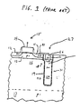
- FIG. 1 An example of a prior an DRAM cell with a buried plate trench cell architecture is shown in FIG. 1.
- a p channel field effect transistor 15 includes an n+ drain well 11, n+ source well 12 and p- channel region 13, which has gate 14 disposed thereon.
- Buried layer 16, here shown doped n+ is disposed within a p-doped substrate 17 beneath the active regions of transistor 15.
- a trench 31 filled with n+ doped polysilicon 54, 56 penetrates the buried layer 16.
- buried region 16 has a portion adjacent to the trench region 31.
- Channel region 13 also has a portion which is adjacent to trench region 31.
- These adjacent portions of buried region 16 and channel region 13 form the other plate of trench capacitor 27.
- Dielectric layer 19 thus separates the two plates of trench capacitor 27.
- the drain well 11 is electrically connected to the trench cell 31 via trench electrode 41. Logic level voltages are thus transferred from the transistor 15 to the trench capacitor 27 which stores the voltage data.
- N+ buried layer 16 acts as the source
- p- region 13 acts like the channel region
- n+ well 11 acts as the drain of the parasitic transistor 18.
- Doped polysilicon 56 acts as the gate
- isolation collar 51 acts as the insulator between the gate and the channel of parasitic transistor 18. The parasitic device 18 must be kept turned off when the trench electrode 41 is at a high logic level voltage. This is accomplished by conveniently forming the isolation collar 51 as a thick oxide or the like, and having it extend down the trench 31 to substantially isolate the adjoining portion of channel region 13 from the doped polysilicon 56.
- the trench 31 is first filled with doped semiconductor material 54 up until a predetermined level near the bottom of the isolation collar 51. This level is indicated by the cross-sectional depth line 29 in FIG. 1.
- the isolation collar 51 is formed, which may be a thick oxide layer such as tetra-ethyl-ortho-silicate (TEOS).
- TEOS tetra-ethyl-ortho-silicate
- the trench 31 is then filled with another "plug" 56 of the same doped semiconductor material from line 29 to the top surface.
- two "plugs" of n+ polysilicon or similar material are needed to fill the trench 31.
- the oxide isolation collar technique while affording a number of advantages, suffers from several drawbacks in the course of subsequent processing.
- One problem is that subsequent high temperature steps will diffuse oxygen through top layers and eventually through the collar. This will lead to trench sidewall silicon oxidation and to poly oxidation, i.e., "trench poly-fill".
- the oxygen diffusion results in volume expansion which in turn can lead to the introduction of stacking faults and dislocations through stress generation.
- Another problem is that contaminants outdiffusing from a TEOS collar may contribute to interface problems between the two semiconductor fill layers within the trench. This can lead to severe contact problems of the trench electrode.
- An additional problem is that outdiffusion of dopants from the highly doped trench polysilicon fill through the collar is possible in the case of disrupted or otherwise damaged collars.
- the instant invention is an improved trench cell capacitor within a semiconductor body, suitable for use in a 64KB DRAM memory cell or in other similar memory cells.
- the improved trench cell capacitor includes a trench cell with doped semiconductor material disposed therein, an oxide isolation collar of a predetermined thickness surrounding the doped semiconductor material, and a nitride layer disposed between the oxide isolation collar and the doped semiconductor material.
- the nitride layer has a thickness less than the predetermined thickness of the isolation collar.
- the inclusion of the nitride layer between the isolation collar and the doped material solves a number of processing problems associated with prior art trench cell capacitors having isolation collars.
- the improved trench cell capacitor may have a second oxide layer disposed between the nitride layer and the doped semiconductor material.
- the trench cell of the capacitor may have a first region and a second region, with the isolation collar and the nitride layer being situated within the first region, and the doped semiconductor material being disposed in both of the first and second regions.
- a dielectric insulating layer having a thickness less than the predetermined thickness of the isolation collar surrounds the doped semiconductor material within the second region and also forms a bottom of the trench cell.
- the trench capacitor preferably has a buried layer of doped semiconductor material adjacent to the trench cell to substantially form one plate of the trench capacitor, wherein the doped semiconductor material disposed within the first and second regions of the trench cell forms a second plate of the capacitor, and the dielectric layer separates the plates of the capacitor.
- the present invention also teaches a method of fabricating an improved trench cell capacitor within a semiconductor body.
- the method comprises the steps of: forming a trench within a semiconductor substrate; depositing an oxide layer of a predetermined thickness on exposed walls within the trench and on an exposed major surface within the trench; depositing a nitride layer over exposed portions of the oxide layer, where the nitride layer has a thickness less than the predetermined thickness; etching away a portion of the nitride layer and of the oxide layer covering the major surface to expose a portion of the major surface; and filling the trench with doped semiconductor material to substantially fill the trench.
- This method may further include the steps of: lining a portion of the trench with a dielectric layer of a given thickness after the trench is formed within the semiconductor substrate, where the given thickness is less than the predetermined thickness; filling the trench to a predetermined level with doped semiconductor material to substantially form the major surface at the predetermined level, the major surface thereby including exposed doped semiconductor material.
- the present invention also teaches a method of fabricating a trench cell capacitor within a semiconductor body, comprising the steps of: forming a trench within a semiconductor body; depositing an oxide layer of a predetermined thickness on exposed walls within the trench and on an exposed major surface within the trench; etching away a portion of the oxide layer covering the major surface to expose a portion of the major surface; depositing a nitride layer over exposed portions of the oxide layer and on the exposed portion of the major surface; etching away a portion of the nitride layer covering the major surface to again expose a portion of the major surface; and filling the trench with doped semiconductor material to substantially fill the trench.
- Figures 1-8 correspond to Figures 1-8 of parent application Serial No. 08/726,442 and Figures 9-15 correspond to Figures 1-7 of parent application Serial No. 08/715,289.
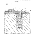
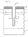
- a preferred embodiment of an improved DRAM according to the instant invention is shown in cross section in FIG. 2.
- a DRAM 20 includes a transistor 36 and a trench capacitor 32 coupled to transistor 36, for storing data.
- Trench capacitor 32 includes a trench cell 21 which has a thick oxide isolation collar 24 formed peripherally along its upper sidewalls.
- a thin nitride liner 25 is disposed on the inner sidewalls of the oxide collar 24. This thin nitride liner 25 is an important feature of the instant invention, as will be described below.
- the DRAM 20 may be formed by growing epitaxial layers on a doped semiconductor substrate 33, as is well known in the art.
- a buried layer 26, typically highly doped, is formed within the substrate 33 either by selective ion implantation or by epitaxial growth. Forming a buried layer in a semiconductor substrate is known in the art. For example, a lower portion of buried layer 26 may be formed within substrate 33 and an upper portion of buried layer 26 may be formed within an epitaxial layer (not shown).
- depth line 43 shows the separation between the buried layer 26 and the channel region 28 of the transistor 36. Also shown is drain well 23, source well 29 and gate 35, which together with channel region 28 comprise the transistor 36.
- DRAM 20 also includes contact region 44, doped region 81 and oxide isolation region 78.
- channel region 28 also extends beneath source and drain wells 29 and 23.
- Channel region 28 is preferably of opposite conductivity as the buried layer 26.
- isolation is provided between the buried layer 26 and the source and drain regions 29 and 23.
- Exemplary doping conductivities are: substrate 33, p- conductivity; buried layer 26, n+; channel 28, p-; drain and source regions 33 and 29, n+; contact region 44, n+; doped region 81, p-.
- the transistor 36 thus formed would then be a p channel FET.
- the instant invention may just as readily be implemented using an n channel FET.
- a side effect of the vertical structure is the formation of a parasitic transistor 45 formed between buried layer 26, drain well 23 and the portion of channel region 28 between regions 23 and 26.
- trench cell 21 of capacitor 32 is formed within the buried layer 26. While trench cell 21 may be substantially cylindrical, it may also be formed with a truncated cone-like shape with the wide portion of the cone being at the top surface. The diameter of the trench cell cone would then taper down to a given diameter at a predetermined depth. Trench cell 21 may also have a square or rectangular platform. It is seen tat the cross-sectional view of FIG. 2 corresponds to either a cylindrical trench or a french with a square or rectangular platform. Whether the trench cell is substantially cylindrical or otherwise, the very bottom of the trench could be formed so that it is recessed out at the bottom to improve punchthrough characteristics.
- a thin dielectric layer 22 is disposed along the bottom of the trench and peripherally along the bottom sidewalls of the trench up to a predetermined level, as indicated by depth line 39.
- Dielectric layer 22 may alternatively extend all the way to the top surface 89 of the DRAM 20 instead of ending at line 39 (this embodiment is omitted from FIG. 2.)
- This dielectric layer 22 may be silicon dioxide (SiO 2 ) such as a thermal oxide or TEOS oxide or multilayers of oxides, nitrides, and/or deoxidized nitride. If the trench cell 21 is formed with a recessed out portion (not shown) at the bottom of the trench, then the oxide layer at the trench bottom would be thicker than that along the sidewalls. This increased oxide thickness at the trench bottom is advantageous because this area is more vulnerable to punchthrough, as has been found in the prior art.
- the trench 21 is filled with a first "plug" 38 of doped polysilicon to the same level as that of the thin oxide layer 22, i.e., to line 39.
- plug 38 is preferably doped n+.
- plug 38 would be doped p type and buried layer 26 would also preferably be p type.
- a second polysilicon plug 37 preferably of the same doping level as the first plug 38, fills the remainder of the trench cell 21. However, this second plug 37 is inserted in the trench after the thick oxide collar 24 and nitride collar 25 are formed, as will be described below.
- Polysilicon plugs 38 and 37 thus form one plate of trench cell capacitor 32.
- buried layer 26 has a portion which adjoins trench cell 21.
- Channel region 28 also has a portion adjoining trench cell 21.
- the combination of these adjoining portions of buried layer 26 and channel 28 form the other plate of capacitor 32, with the substantial contribution coming from the buried plate adjoining portion.
- the adjoining portion of channel 28 contributes very little to the capacitance.
- Thin dielectric layer 22 thus separates the plates of the capacitor 32. The thinner dielectric layer 22 is made, the higher the capacitance. However, layer 22 must be made thick enough to ensure that no dielectric breakdown will occur.
- a parasitic transistor 45 is formed as follows: buried layer 26 acts as the drain, drain region 23 acts as the source, polysilicon 37 behaves as the gate, and the portion of channel region 28 between regions 23 and 26 acts as the channel region for parasitic transistor 45. Oxide collar 24 with nitride liner 25 behaves as the insulator between the gate and the channel of parasitic transistor 45. The combination of the thickness of oxide collar 24, which functions to increase the threshold voltage of the parasitic device, and the low conductivity doping of channel region 28, insures that parasitic transistor 45 is not conductive.
- thick oxide collar 24 An additional purpose of the thick oxide collar 24 is to assure that there is no dielectric breakdown or punchthrough between polysilicon 37 and region 28. Dielectric breakdown or punchthrough would otherwise be a possibility whenever a high differential voltage is present between polysilicon 37 and the portion of channel 28 that adjoins the trench 21.
- nitride layer or "liner" 25 on the inner sidewalls of oxide isolation collar 24 affords several key advantages over a trench cell capacitor without such a nitride liner. Firstly, subsequent high temperature processing and high temperature oxidation is customarily performed after the formation of the isolation collar 24. The nitride liner 25 prevents excess oxidation of the trench-fill polysilicon (plugs 37 and 38) which would otherwise occur during the subsequent processing. Second, nitride liner 25 also prevents trench sidewall bulk silicon oxidation that would otherwise occur during the high temperature oxidation.
- nitride liner 25 functions to prevent outdiffusion of dopants from the highly doped regions 37 and 38 through "weak" regions of the isolation collar 24 into the vertical parasitic device 45. This outdiffusion would typically undesirably turn on the parasitic device 45 or cause it to exhibit leakage, problems which are now prevented by the nitride liner 25.
- nitride liner 25 prevents interface contamination between trench fill polysilicon plugs 38 and 37. This is accomplished by the nitride liner 25 hindering outdiffusion and outgassing of contaminants such as oxygen from the isolation collar region during trench polysilicon fill with plug 37 and associated processing.
- trench cell 21 may have another thin oxide liner (omitted from FIG. 2 for convenience) disposed peripherally on the inner sidewalls 79 of nitride liner 25, i.e., between nitride liner 25 and polysilicon plug 37.
- This thin oxide liner may be formed by heat treating the nitride liner 25 at a high temperature such as, for example, 900° Celcius under a steam atmosphere.
- liner 25 comprised of silicon nitride
- a thin layer of the inner walls of nitride liner 25 is convened to SiO 2 by this heat treatment to form the thin oxide liner.
- a thick oxide layer 55 is formed, as shown in FIG. 3.
- Oxide layer 55 is formed to cover a major surface indicated by line 39, consisting of the top surfaces of first silicon plug 38 and of thin dielectric layer 22.
- Layer 55 extends peripherally along the upper sidewalls of trench 21 and along the top surfaces of wells 23 and 44.
- Thick oxide layer 55 may be a silicon dioxide which is preferably a TEOS oxide, but may also be a thermal oxide.
- Nitride layer 57 is then deposited to cover all exposed areas of thick oxide layer 55 within trench 21 along the sidewalls and above line 39, and also to cover exposed areas above regions 23 and 44, as shown.
- Nitride layer 57 is preferably a silicon nitride such as Si 3 N 4 and deposited either by low pressure chemical vapor phase deposition (LPCVD), by CVD, or by PECVD or other appropriate method.
- An exemplary thickness of nitride layer 55 would be in the range of 70-180 angstroms.
- An exemplary thickness of oxide layer 55 is preferably three to five times the thickness of the nitride layer. It is noted that thin dielectric layer 22 may be about the same thickness as the nitride layer 55, i.e., 70-180 Angstroms.
- nitride layer 57 and thick oxide layer 55 disposed on the top surface of polysilicon plug 38 and within the inner sidewalls of nitride layer 56 are then etched away. Standard photomasking and photoetching techniques may be used as well as spacer-forming plasma etching techniques.
- the layers above regions 23 and 44 are also etched away. Thick oxide collar 24 with thin nitride liner 25 are thus formed, as shown in FIG. 4. Precautions must be taken during the etching process to prevent the portion of nitride layer 57 that is disposed on the inner sidewalls of oxide layer 55 from being substantially consumed.
- Photoetching is also used to peripherally etch back oxide layer 24 and nitride liner 25 from the top surface down, to form a peripherally tapered region 52.
- This allows the second polysilicon plug 37 (shown in FIG. 2), which is subsequently formed or inserted, to be situated closer to drain region 23, thereby facilitating electrical contact between the two regions.
- the etching back technique thus obviates the need for an additional electrode between the trench polysilicon plug 37 and drain 23 by enabling a direct electrical connection between the two regions, or, allows for the use of a physically smaller electrode.
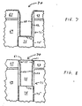
- FIG. 5 shows a trench capacitor 70 comprising a trench cell 71 formed within a buried layer 69.
- the bottom portion of trench 71 is lined peripherally with a thin dielectric layer 75, and filled with a first highly doped polysilicon plug 76 up to a predetermined depth line 72.
- a thick oxide layer 62 such as TEOS is then formed along the upper sidewalls of trench 71, and on a major surface consisting of the top surfaces of polysilicon plug 76 and thin oxide layer 75, which is indicated by depth line 72.
- Oxide layer 62 is also formed to extend on the top surfaces of drain region 67 and doped region 63. Layer 62 is then "spacer" etched away in the region above depth line 72 such that only the thick oxide sidewalls remain, as shown in FIG. 6. The portion of thick oxide layer 62 above regions 67 and 63 are also etched away and the top portion etched back to form a peripherally tapered region 61.
- a thin nitride layer 60 is then applied within trench 71 to completely cover thick oxide layer 62, as shown in FIG. 7.
- An exemplary thickness of nitride layer 60 would be 70 to 180 Angstroms.
- Thick oxide layer 62 may be, for example, three to five times the thickness of nitride layer 60.
- Dielectric layer 75 is preferably about the same order of thickness of nitride layer 60.
- Nitride layer 60 which may be silicon nitride Si 3 N 4 deposited by LPCVD, CVD, PECVD or other appropriate method, initially covers the top surfaces of regions 67 and 63 and the exposed surface of polysilicon plug 76, corresponding to depth line 72.
- a tapered nitride layer region 77 is also formed in proximity to tapered oxide region 61 via the spacer etching. This allows drain region 67 to be situated closer to a second highly doped polysilicon plug 75, which is formed or inserted within trench cell 71 as the last step in the process. Electrical contact between the two regions is thereby facilitated or may be accomplished directly.
- the resulting nitride liner 60 extends all the way down to the first polysilicon plug 76 at depth line 72. This is slightly different than the structure of FIG. 4 which was the result of the first described process according to the present invention.
- the nitride liner 25 extends down to a depth 58 which is slightly shallower than the depth of oxide collar 24.
- the alternate described process corresponding to FIGs. 5-8 has one advantage over the process of FIGs. 3-4. That is, consumption of the nitride layer 60 is more easily avoided by etching the oxide layer disposed on the major polysilicon surface in a separate step, i.e., as shown in FIG. 6.
- the potion of the nitride layer 57 disposed on the sidewalls of oxide layer 55 may be undesirably subjected to relatively more etching in order to etch away the oxide layer disposed on plug 38.
- this sidewall portion of nitride layer 57 is more easily consumed.
- the process of FIGs. 5-8 involves more steps, and hence, it is necessary for the trench capacitor designer to perform a tradeoff between the two processes.
- a first advantage of the capacitor according to the instant invention is that excess oxidation of trench-fill doped polysilicon is prevented during high temperative processing subsequent to isolation collar formation.
- Another advantage of this invention is that trench sidewall bulk silicon oxidation is prevented during high temperature oxidation.
- a further advantage of the present invention is that, by preventing unwanted oxidation, the generation of stress induced defects are in turn prevented.
- An additional advantage of this invention is that it prevents the outdiffision of dopants through "weak" collar regions into regions of a vertical parasitic device adjacent to the trench cell capacitor, which would otherwise be turned on or exhibit leakage.
- Yet another advantage of the instant invention is that contamination of the interface between two polysilicon "plugs" that fill the trench cell of the capacitor is prevented.
- the invention prevents this contamination by hindering outdiffusion and outgassing of contaminants such as oxygen from the isolation collar region during the trench poly-fill and processing that occurs after the isolation collar is formed.
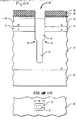
- a buried layer 12 is formed within a silicon substrate 10 and doped to a N+ impurity concentration. Buried layer 12 may be formed via selective ion implantation, epitaxial growth or a combination of both, as is commonly known in the art. This buried layer 12 will constitute one of the plates of the trench cell capacitor. Atop the buried layer 12, silicon layers 14 and 16 are epitaxially grown and doped P- and N+, respectively. It should be understood that opposite conductivities to those illustrated may be employed, as is known by those skilled in the art. Layers 14 and 16 form the channel and drain regions, respectively of an FET (not shown) which transfers logic level voltages to the trench capacitor to be formed.
- oxide layer 18 and silicon nitride layer 20 are then sequentially deposited on the top surface of the structure, which layers are patterned via a conventional etching method to form an opening 15 that exposes the top surface of the drain region 16.
- the oxide layer 18 may be either tetra-ethyl-ortho-silicate (TEOS), or silicon dioxide formed by thermal oxidation.
- Silicon nitride layer 20 may be Si 3 N 4 deposited using LPCVD or plasma enhanced chemical vapor deposition (PECVD). Exemplary thicknesses for the layers are 50-100nm for the oxide layer 18, and about 300nm for the silicon nitride layer 20.
- Layers 18 and 20 serve as a hard mask for the formation of a trench within the opening 15.
- the silicon nitride layer 20 acts as an oxidation barrier to protect the top surface of the device during trench sidewall oxidation (to be described below).
- the exposed silicon in the opening 15 is reactively ion etched in an atmosphere containing SF 6 , Cl 2 and He to form a deep trench 22 as shown in FIGs. 10A and 10B.
- Other suitable atmospheres may alternatively be employed in the etching process.
- Trench 22 is thus formed by etching through the epitaxial layers 16 and 14 and through a substantial portion of the buried layer 12.
- the trench 22 has an exemplary depth of five microns, and an exemplary width W of 250-500nm.
- Peripheral shoulders 26 define a lower portion 27 and upper portion 24 of the trench 22, where lower portion 27 has a smaller width than that of the upper portion 24.
- the trench 22 may have a rectangular platform; however, the trench platform geometry may be tailored as desired for a particular application.
- the trench 22 is formed with substantially vertical sidewalls.
- Dielectric layer 28 is then formed along the sidewalls and bottom of the trench 22.
- Dielectric layer 28 preferably has a thickness in the range of 10-50nm, and is composed of silicon dioxide formed by thermal oxidation.
- dielectric layer 28 may be composed of a three layer oxide/nitride/oxide sandwich.
- the layer 28 serves as the dielectric separating the two plates of the trench capacitor. The thinner that layer 28 is made, the higher the capacitance, as is commonly known.
- the thickness of layer 28 at the bottom of the trench may be greater than along the sidewalls in order to reduce the possibility of punch-through at the bottom of the trench.
- a first polysilicon "fill" plug 30 is formed by directional LPCVD to completely fill the lower portion 27 and a part of the upper portion 24 of the trench 22.
- Directional LPCVD is used with an ion beam impinging the device structure at normal incidence. This allows the trench to be filled with polysilicon essentially from the bottom up, without polysilicon being deposited on the upper sidewalls of the trench.
- a low temperature of less than about 750°C is used in this process.
- An example of a suitable apparatus for such directional LPCVD is found in U.S. Patent No. 5,290,358 entitled “Apparatus for Directional Low Pressure Chemical Vapor Depositor (DLPCVD)".
- the fill plug 30 is highly doped with arsenic to provide a N+ impurity concentration in the illustrative embodiment.
- the doping of the fill plug 30 can be accomplished either during the LPCVD, or in a subsequent step via ion implantation.
- Polysilicon fill 30 thus forms the second plate of the trench capacitor--the first plate consists of the buried layer 12 in the immediate vicinity of the lower portion of the trench 22.
- the fill plug 30 will of course also be doped P+ using a suitable doping agent such as boron.
- Fill 30 extends up from the bottom of the trench, above the trench shoulders 26, to a depth level of approximately one to two microns below the top surface of the silicon layer 16--thus, it has a vertical length of about three to four microns.
- a thick oxide layer 32 composed of TEOS or silicon dioxide, is formed peripherally around the remaining sidewalls of the trench 22, and on the top surface of the fill plug 30, as shown in FIG. 13A.
- the oxide layer 32 extends over the top of the trench 22 to overlay the nitride layer 20.
- An exemplary thickness for this layer 32 is in the range of 50-100nm.
- a 5-20nm thick silicon nitride layer 33 such as Si 3 N 4 is deposited using, for example, LPCVD, CVD or PECVD.
- the total thickness of an isolation "collar” consisting of dielectric layer 28 together with oxide layer 32 and nitride layer 33 is in the range of about 65-170nm (assuming a thickness range of 10-50nm for dielectric layer 28).
- the addition of the nitride layer 33 affords several advantages. These include preventing excessive oxidation of the doped polysilicon within the trench during subsequent high temperature processing; and preventing outdiffusion of dopants through weak collar regions into regions of the vertical parasitic device adjacent to the trench cell capacitor, which would otherwise be turned on or exhibit leakage. Despite the aforementioned advantages, it should be understood that the additional nitride layer 33 may be eliminated if so desired, to reduce the complexity of the overall process.
- the bottom portions of oxide layer 32 and nitride layer 33 in the center of the trench are then etched away to expose the top portion of the polysilicon fill plug 30 as is shown in FIG. 13B.
- the portions of layers 32 and 33 overlaying the nitride layer 20 are also etched away at this time.
- a directional etch such as reactive ion etch (RIE) is preferably employed.
- RIE reactive ion etch
- a small recess 35 is intentionally formed in the fill plug 30, which serves as a foundation for the polysilicon epitaxial growth to be described. Precautions must be taken in the etching step to prevent the nitride layer 33 on the sidewalls from being substantially consumed.
- this etching of the bottom portion of the isolation collar often consumes some of the isolation collar sidewalls, resulting in a tapered trench.
- the integrity of the polysilicon fill within the upper portion of the trench is highly dependent upon the trench shape and thus, the etching process has to be closely controlled to keep the shape within a narrow tolerance window.
- the selective epitaxial growth of the trench polysilicon to be described is relatively independent of trench shape. This allows for a broader process window for the preceding isolation collar etching step.
- a second polysilicon fill plug 36 is grown on the first fill plug 30 by means of selective epitaxial growth. This epitaxial growth of the second fill 36 is a key aspect of the present invention.
- the selective epitaxial growth occurs from the bottom up, i.e., from the recess of the first fill 30 to the top portion of the oxide layer 32, resulting in a void free polysilicon fill.
- the polysilicon fill 36 is doped to a N+ impurity level either by using in-situ doped selective epitaxy or by using intrinsic selective epitaxy followed by an ion implantation step.
- the doping agent is preferably arsenic to achieve this N+ doping concentration.
- the second fill 36 will of course also be doped P+.
- the selective epitaxial growth process for forming the second fill plug 36 replaces prior art processes which utilized LPCVD.
- a variety of problems with the LPCVD process are obviated with the selective epitaxial growth. These include the problems of voids and seams resulting from the LPCVD which lead to conductive stringers and residues formed during subsequent gate electrode patterning.
- the polysilicon is epitaxially grown in the trench to form the fill plug 36 by using a gas-solid or heterogeneous reaction system.
- the heterogeneous reaction system preferably employs a combination of gases including H 2 , SiCl 4 , HCl and a dopant gas containing arsenic to provide a N+ doping level. (When a P+ doping concentration is desired, a dopant gas containing boron is used).
- the dopant gas may be excluded and the fill plug 36 doped to the desired impurity level using selective ion implantation with appropriate masking after the epitaxial growth is complete. In this latter case, the ion implantation can be tailored to dope the first polysilicon fill plug 30 at the same time, provided that the fill plug 30 was not already doped, of course.
- the epitaxial growth process is performed at a temperature within the range of about 900-1100°C. Since the portion of the trench 22 to be filled via epitaxial growth is deep--typically between 1.0-2.0 microns--this rapid filling of the trench is highly desirable.
- the epitaxial growth occurs vertically to a level protruding above the top surface of silicon layer 16, as shown. Also, the device is subjected to the high ambient temperature for at least several minutes prior to the epitaxial growth in a pre-bake step. This pre-bake enhances the integrity of the interface between the fill 30 and the fill 36 at the recess 35. A low contact resistance is thus provided at that interface.
- the hard mask layers 20 and 18 are selectively etched to expose a portion of the well region 16.
- a contact electrode 37 is then formed using suitable metallization to interconnect the top surface of the polysilicon fill plug 36 and the exposed surface of the well region 16. Such contact electrode formation is well known in the art.
- an improved process for fabricating a trench cell capacitor which utilizes selective epitaxial growth to form the top polysilicon fill layer within the trench.
- the process according to the invention results in an improved trench cell capacitor with less voids and seams in the trench polysilicon as compared to trench capacitors fabricated using the CVD processes of the prior art. Residue and stringer formation problems during subsequent gate electrode patterning are eliminated with the present invention.
- the softer and void free surfaces of the epitaxially grown trench polysilicon enhances the robustness of the memory cell, allowing a broader process window for subsequent oxidations.
- the process of the present invention is also simpler than the prior art inasmuch as it eliminates the need for trench polysilicon and isolation collar annealing, chemical mechanical polishing (CMP), cleans, and trench fill recess steps. Moreover, the risk of thinning the oxide/nitride hard mask during CMP is eliminated. Finally, a broader process window for the trench etching is provided because the epitaxially grown wench polysilicon is highly robust independent of the trench shape.
Landscapes
- Engineering & Computer Science (AREA)
- Manufacturing & Machinery (AREA)
- Semiconductor Memories (AREA)
Abstract
Description
Claims (29)
- A method of fabricating a trench cell capacitor within a semiconductor body, the method comprising:forming a trench within a semiconductor substrate, wherein the trench comprises upper and lower portions;lining the trench with a dielectric layer;after lining the trench, forming a collar in an upper portion of the trench by forming an oxide layer in the upper portion of the trench and a nitride layer on the oxide layer; andfilling said trench with semiconductor material to substantially fill said trench.
- The method of claim 1 and further comprising filling the lower portion of the trench with a conductive material before forming the collar.
- The method of claim 2 wherein filling the lower portion of the trench comprises filling the lower portion of the trench with polysilicon.
- The method of claim 1 and further comprising subjecting the nitride layer to a heat treatment in the presence of steam such that an exposed surface of said nitride layer is converted to a second oxide layer.
- The method of claim 1 wherein the oxide layer is deposited within the trench on exposed walls of the trench and on an exposed major surface within the trench and the nitride layer is deposited on exposed portions of the oxide layer.
- The method of claim 5 and further comprising etching away a portion of the nitride layer and a portion of the oxide layer disposed on the major surface to expose a portion of the major surface.
- The method of claim 6 and further comprising etching away a top portion of the oxide layer and of the nitride layer, the top portion of the oxide layer being disposed on the walls of the trench, wherein the oxide layer and the nitride layer are tapered as a function of depth such that the top portion of the oxide layer has a thickness that is less than a remaining portion of the oxide layer and such that the tip portion of the nitride layer has a thickness that is less than a remaining portion of the nitride layer.
- The method of claim 1 and further comprising prior to forming the collar:lining the lower portion of the trench with a dielectric layer after the trench is formed within the semiconductor substrate, the dielectric layer serving as the node dielectric of the trench capacitor; andproviding the trench with doped semiconductor material in the lower portion thereof.
- The method of claim 1 wherein:the oxide layer is deposited on exposed walls of the upper portion of the trench and on an exposed major surface within the trench;a portion of the oxide layer covering the major surface is etched away to expose a portion of the major surface;the nitride layer is deposited within the trench over exposed portions of the oxide layer and over exposed portions of the major surface; anda portion of the nitride layer deposited on the major surface is etched away to again expose a portion of the major surface.
- The method of claim 1 wherein:the oxide layer is deposited on exposed walls of the upper portion of the trench and on an exposed major surface within the trench;the nitride layer is deposited within the trench over exposed portions of the oxide layer; andportions of the oxide layer and the nitride layer deposited on the major surface is etched away to expose a portion of the major surface.
- The method of claim 1 wherein the nitride layer is Si3N4deposited by chemical vapor deposition.
- The method of claim 1 wherein the trench capacitor is formed as part of a dynamic random access memory cell.
- The method of claim 1 wherein filling the trench comprises epitaxially growing a semiconductor material in the upper portion of the trench.
- A method of fabricating a trench cell capacitor within a semiconductor body, the method comprising:forming a trench within a semiconductor substrate, wherein the trench comprises upper and lower portions;forming a dielectric layer upon a surface of both the upper and lower portions of the trench;filling the lower portion of the trench with a conductive material;forming a collar in the upper portion of the trench, the collar comprising an oxide layer and a nitride layer; andfilling the upper portion of the trench with a conductive material.
- The method of claim 14 wherein the step of forming a collar comprises:depositing the oxide layer on a surface of the upper portion of the trench;depositing the nitride layer on the oxide layer; andsubjecting the nitride layer to a heat treatment in the presence of steam such that an exposed surface of said nitride layer is converted to a second oxide layer.
- The method of claim 14 wherein the step of forming a collar comprises:depositing the oxide layer on a surface of the upper portion of the trench; anddepositing the nitride layer on the oxide layer;
wherein a portion of the oxide layer is removed prior to depositing the nitride layer, the portion of the oxide layer being disposed over the conductive material in the lower portion of the trench. - The method of claim 14 wherein the step of forming a collar comprises:depositing the oxide layer on a surface of the upper portion of the trench; anddepositing the nitride layer on the oxide layer;
wherein a portion of the oxide layer is removed after depositing the nitride layer, the portion of the oxide layer being disposed over the conductive material in the lower portion of the trench. - The method of claim 14 wherein the steps of filling the lower portion and the upper portion of the trench both comprise filling the trench with a doped semiconductor material.
- The method of claim 14 wherein filling the upper portion of the trench with a conductive material comprises epitaxially growing a semiconductor material in the upper portion of the trench.
- A method of forming a trench capacitor, the method comprising:forming a trench in a semiconductor region, the trench including upper and lower portions;lining the upper and lower portions of the trench with a dielectric material;filling the lower portion of the trench with a conductive material;forming an oxide layer over the semiconductor region, surfaces of the dielectric layer on the upper portion of the trench and exposed portions of the conductive material in the lower portion of the trench;anisotropically etching the oxide layer to remove portions of the oxide layer over the semiconductor region and over the conductive material in the lower portion of the trench;forming a nitride layer over the semiconductor region, the oxide layer on the upper portion of the trench, and exposed portions of the conductive material in the lower portion of the trench;anisotropically etching the nitride layer to remove portions of the nitride layer over the semiconductor region and over the conductive material in the lower portion of the trench; andfilling the upper portion of the trench with a conductive material.
- The method of claim 20 wherein filling the upper portion of the trench with a conductive material comprises epitaxially growing a semiconductor material in the upper portion of the trench.
- The method of claim 20 and further comprising the step of forming a second oxide layer over the nitride layer prior to anisotropically etching the nitride layer.
- The method of claim 22 wherein the second oxide layer is formed by subjecting the nitride layer to a heat treatment in the presence of steam.
- The method of claim 20 and further comprising subjecting the nitride layer to a heat treatment in the presence of steam such that an exposed surface of the nitride layer is converted to a second oxide layer.
- The method of claim 20 wherein:filling the lower portion of the trench comprises filling the lower portion of the trench with a doped semiconductor material; andfilling the upper portion of the trench comprises filling the upper portion of the trench with a doped semiconductor material.
- In a process for fabricating a trench cell capacitor having a trench penetrating a doped buried layer within a semiconductor body, said doped buried layer forming a first plate of said capacitor, said trench having a lower portion filled with doped semiconductor material to partially form a second plate of said capacitor, and a peripheral dielectric layer separating said first capacitor plate and said second partially formed capacitor plate, the improvement therewith comprising the steps of:forming an isolation collar in a top portion of said trench, said isolation collar comprising a layer of nitride deposited on a layer of oxide; andfilling said top portion of said trench in a region surrounded by said isolation collar with a conductive material.
- The process of claim 26 wherein filling said top portion of said trench comprises epitaxially growing semiconductor material to complete said second plate of said capacitor.
- A process for fabricating a trench cell capacitor within a silicon substrate, comprising the steps of:forming a doped buried layer within said silicon substrate to provide a first plate of said capacitor;forming a trench within said silicon substrate to a depth level penetrating the buried layer;depositing a dielectric layer peripherally within said trench;filling a lower portion of said trench with doped polysilicon to partially form a second plate of said capacitor, wherein said first plate and second partially formed plate are separated by said dielectric layer;forming an isolation collar peripherally within an upper portion of said trench, said isolation collar comprising a layer of nitride deposited on a layer of oxide; andforming silicon material within said isolation collar, said polysilicon completing said second plate of said capacitor.
- The process of claim 28 wherein forming polysilicon material within said isolation collar comprises epitaxially growing silicon within said isolation collar.
Applications Claiming Priority (2)
| Application Number | Priority Date | Filing Date | Title |
|---|---|---|---|
| US282122 | 1981-07-10 | ||
| US09/282,122 US6207494B1 (en) | 1994-12-29 | 1999-03-31 | Isolation collar nitride liner for DRAM process improvement |
Publications (2)
| Publication Number | Publication Date |
|---|---|
| EP1041623A2 true EP1041623A2 (en) | 2000-10-04 |
| EP1041623A3 EP1041623A3 (en) | 2001-04-11 |
Family
ID=23080198
Family Applications (1)
| Application Number | Title | Priority Date | Filing Date |
|---|---|---|---|
| EP00104798A Withdrawn EP1041623A3 (en) | 1999-03-31 | 2000-03-06 | An isolation collar nitride liner for DRAM process improvement |
Country Status (6)
| Country | Link |
|---|---|
| US (1) | US6207494B1 (en) |
| EP (1) | EP1041623A3 (en) |
| JP (1) | JP2000294747A (en) |
| KR (1) | KR20000076992A (en) |
| CN (1) | CN1279509A (en) |
| TW (1) | TW468239B (en) |
Cited By (2)
| Publication number | Priority date | Publication date | Assignee | Title |
|---|---|---|---|---|
| DE10151198A1 (en) * | 2001-10-17 | 2003-05-08 | Infineon Technologies Ag | Producing an isolation collar in trench structure of semiconductor component comprises forming first layer on substrate, forming trench in the first layer; partially filling the trench with filling material and further processing |
| CN102723277A (en) * | 2009-08-31 | 2012-10-10 | 万国半导体股份有限公司 | Fabrication of trench dmos device having thick bottom shielding oxide |
Families Citing this family (51)
| Publication number | Priority date | Publication date | Assignee | Title |
|---|---|---|---|---|
| US6034417A (en) * | 1998-05-08 | 2000-03-07 | Micron Technology, Inc. | Semiconductor structure having more usable substrate area and method for forming same |
| US6307247B1 (en) * | 1999-07-12 | 2001-10-23 | Robert Bruce Davies | Monolithic low dielectric constant platform for passive components and method |
| DE19941147A1 (en) * | 1999-08-30 | 2001-03-22 | Infineon Technologies Ag | Production of epitaxial layer for dynamic random access memory comprises preparing substrate having single crystalline and insulated regions, growing epitaxial layer on single crystalline region and partially removing epitaxial layer |
| US6344415B1 (en) * | 1999-09-15 | 2002-02-05 | United Microelectronics Corp. | Method for forming a shallow trench isolation structure |
| US6271080B1 (en) * | 1999-12-16 | 2001-08-07 | International Business Machines Corporation | Structure and method for planar MOSFET DRAM cell free of wordline gate conductor to storage trench overlay sensitivity |
| DE10014920C1 (en) * | 2000-03-17 | 2001-07-26 | Infineon Technologies Ag | Production of a trench capacitor comprises filling a trench with a filler, forming an insulating collar, removing the filler, forming a trenched plate using low pressure gas phase doping, etc. |
| DE10027913A1 (en) * | 2000-05-31 | 2001-12-13 | Infineon Technologies Ag | Memory cell with a trench capacitor |
| US6358785B1 (en) * | 2000-06-06 | 2002-03-19 | Lucent Technologies, Inc. | Method for forming shallow trench isolation structures |
| US6573137B1 (en) * | 2000-06-23 | 2003-06-03 | International Business Machines Corporation | Single sided buried strap |
| DE10045694A1 (en) * | 2000-09-15 | 2002-04-04 | Infineon Technologies Ag | Semiconductor memory cell with trench capacitor and selection transistor and method for its production |
| KR100382722B1 (en) * | 2000-11-09 | 2003-05-09 | 삼성전자주식회사 | Trench isolation layer and manufacturing method thereof |
| JP2002289816A (en) * | 2001-03-23 | 2002-10-04 | Toshiba Corp | Semiconductor device and manufacturing method thereof |
| KR100407567B1 (en) * | 2001-04-10 | 2003-12-01 | 삼성전자주식회사 | Trench Isolation Process Without Dent |
| US6551874B2 (en) * | 2001-06-22 | 2003-04-22 | Infineon Technologies, Ag | Self-aligned STI process using nitride hard mask |
| JP4499967B2 (en) * | 2001-09-18 | 2010-07-14 | セイコーインスツル株式会社 | Manufacturing method of semiconductor integrated circuit |
| US6551893B1 (en) * | 2001-11-27 | 2003-04-22 | Micron Technology, Inc. | Atomic layer deposition of capacitor dielectric |
| KR100417211B1 (en) * | 2001-12-20 | 2004-02-05 | 동부전자 주식회사 | Method of making metal wiring in semiconductor device |
| KR100442781B1 (en) * | 2001-12-24 | 2004-08-04 | 동부전자 주식회사 | semiconductor having having trench capacitor and method for fabricating the same |
| US6573136B1 (en) * | 2002-05-30 | 2003-06-03 | Infineon Technologies Ag | Isolating a vertical gate contact structure |
| DE10225941A1 (en) * | 2002-06-11 | 2004-01-08 | Infineon Technologies Ag | Process for filling trench and relief geometries in semiconductor structures |
| DE10234952B3 (en) * | 2002-07-31 | 2004-04-01 | Infineon Technologies Ag | Production of a semiconductor structure used as a trench capacitor comprises preparing a semiconductor substrate, and forming a trench in the substrate |
| US6734059B1 (en) * | 2002-11-19 | 2004-05-11 | Infineon Technologies Ag | Semiconductor device with deep trench isolation and method of manufacturing same |
| JP2005101352A (en) * | 2003-09-25 | 2005-04-14 | Toshiba Corp | Trench capacitor and manufacturing method thereof |
| TWI229414B (en) * | 2003-10-03 | 2005-03-11 | Promos Technologies Inc | Method of fabricating deep trench capacitor |
| JP4044525B2 (en) * | 2004-01-07 | 2008-02-06 | 株式会社東芝 | Semiconductor memory device and manufacturing method thereof |
| US7410864B2 (en) * | 2004-04-23 | 2008-08-12 | Infineon Technologies Ag | Trench and a trench capacitor and method for forming the same |
| KR100519801B1 (en) * | 2004-04-26 | 2005-10-10 | 삼성전자주식회사 | Semiconductor devices having a nod contact plug surrounded by a stress buffer spacer and methods of fabricating the same |
| US7633110B2 (en) * | 2004-09-21 | 2009-12-15 | Taiwan Semiconductor Manufacturing Co., Ltd. | Memory cell |
| US7274073B2 (en) | 2004-10-08 | 2007-09-25 | International Business Machines Corporation | Integrated circuit with bulk and SOI devices connected with an epitaxial region |
| DE102004049667B3 (en) * | 2004-10-12 | 2006-05-18 | Infineon Technologies Ag | A manufacturing method for a trench capacitor with an insulation collar, which is electrically connected on one side to a substrate via a buried contact, in particular for a semiconductor memory cell and a corresponding trench capacitor |
| TWI278069B (en) * | 2005-08-23 | 2007-04-01 | Nanya Technology Corp | Method of fabricating a trench capacitor having increased capacitance |
| US7709320B2 (en) * | 2006-06-28 | 2010-05-04 | International Business Machines Corporation | Method of fabricating trench capacitors and memory cells using trench capacitors |
| CN100495686C (en) * | 2006-07-27 | 2009-06-03 | 联华电子股份有限公司 | Capacitor contact structure and process for dynamic random access memory |
| US7615480B2 (en) * | 2007-06-20 | 2009-11-10 | Lam Research Corporation | Methods of post-contact back end of the line through-hole via integration |
| US7750412B2 (en) * | 2008-08-06 | 2010-07-06 | Fairchild Semiconductor Corporation | Rectifier with PN clamp regions under trenches |
| US8314471B2 (en) * | 2009-11-17 | 2012-11-20 | Diodes Incorporated | Trench devices having improved breakdown voltages and method for manufacturing same |
| US8030157B1 (en) * | 2010-05-18 | 2011-10-04 | International Business Machines Corporation | Liner protection in deep trench etching |
| US8207032B2 (en) | 2010-08-31 | 2012-06-26 | Micron Technology, Inc. | Methods of forming pluralities of vertical transistors, and methods of forming memory arrays |
| US20150187701A1 (en) | 2013-03-12 | 2015-07-02 | Taiwan Semiconductor Manufacturing Company, Ltd. | Semiconductor Devices and Methods of Manufacture Thereof |
| US9076715B2 (en) | 2013-03-12 | 2015-07-07 | Taiwan Semiconductor Manufacturing Company, Ltd. | Interconnect structure for connecting dies and methods of forming the same |
| US10056353B2 (en) | 2013-12-19 | 2018-08-21 | Taiwan Semiconductor Manufacturing Company, Ltd. | 3DIC interconnect apparatus and method |
| US9412719B2 (en) * | 2013-12-19 | 2016-08-09 | Taiwan Semiconductor Manufacturing Company, Ltd. | 3DIC interconnect apparatus and method |
| US9425150B2 (en) | 2014-02-13 | 2016-08-23 | Taiwan Semiconductor Manufacturing Company, Ltd. | Multi-via interconnect structure and method of manufacture |
| US9543257B2 (en) | 2014-05-29 | 2017-01-10 | Taiwan Semiconductor Manufacturing Company, Ltd. | 3DIC interconnect devices and methods of forming same |
| US9455158B2 (en) | 2014-05-30 | 2016-09-27 | Taiwan Semiconductor Manufacturing Company, Ltd. | 3DIC interconnect devices and methods of forming same |
| US9449914B2 (en) | 2014-07-17 | 2016-09-20 | Taiwan Semiconductor Manufacturing Company, Ltd. | Stacked integrated circuits with redistribution lines |
| US12414350B2 (en) | 2019-09-10 | 2025-09-09 | Korea Electrotechnology Research Institute | Trench-gate sic mosfet device and manufacturing method therefor |
| US11594597B2 (en) * | 2019-10-25 | 2023-02-28 | Taiwan Semiconductor Manufacturing Company, Ltd. | Selective polysilicon growth for deep trench polysilicon isolation structure |
| CN111370297A (en) * | 2020-04-02 | 2020-07-03 | 上海华虹宏力半导体制造有限公司 | How to make a super junction |
| CN113764579B (en) | 2020-06-04 | 2023-06-30 | 长鑫存储技术有限公司 | Capacitor structure, manufacturing method thereof and memory |
| US20230411302A1 (en) * | 2022-06-15 | 2023-12-21 | Texas Instruments Incorporated | Deep trench bypass capacitor for electromagnetic interference noise reduction |
Family Cites Families (11)
| Publication number | Priority date | Publication date | Assignee | Title |
|---|---|---|---|---|
| US4649625A (en) * | 1985-10-21 | 1987-03-17 | International Business Machines Corporation | Dynamic memory device having a single-crystal transistor on a trench capacitor structure and a fabrication method therefor |
| US4728623A (en) * | 1986-10-03 | 1988-03-01 | International Business Machines Corporation | Fabrication method for forming a self-aligned contact window and connection in an epitaxial layer and device structures employing the method |
| KR910008830B1 (en) * | 1988-08-18 | 1991-10-21 | 현대전자산업 주식회사 | Trench sidewall doping method using oxide and nitride walls and semiconductor device |
| US5182224A (en) * | 1988-09-22 | 1993-01-26 | Hyundai Electronics Industries Co., Ltd. | Method of making dynamic random access memory cell having a SDHT structure |
| JP2994110B2 (en) * | 1991-09-09 | 1999-12-27 | 株式会社東芝 | Semiconductor storage device |
| US5283453A (en) * | 1992-10-02 | 1994-02-01 | International Business Machines Corporation | Trench sidewall structure |
| US5434109A (en) * | 1993-04-27 | 1995-07-18 | International Business Machines Corporation | Oxidation of silicon nitride in semiconductor devices |
| JP3480745B2 (en) * | 1993-09-16 | 2003-12-22 | 株式会社東芝 | Method for manufacturing semiconductor device |
| US5677219A (en) * | 1994-12-29 | 1997-10-14 | Siemens Aktiengesellschaft | Process for fabricating a DRAM trench capacitor |
| US5658816A (en) * | 1995-02-27 | 1997-08-19 | International Business Machines Corporation | Method of making DRAM cell with trench under device for 256 Mb DRAM and beyond |
| EP0735581A1 (en) * | 1995-03-30 | 1996-10-02 | Siemens Aktiengesellschaft | DRAM trench capacitor with insulating collar |
-
1999
- 1999-03-31 US US09/282,122 patent/US6207494B1/en not_active Expired - Lifetime
-
2000
- 2000-03-06 EP EP00104798A patent/EP1041623A3/en not_active Withdrawn
- 2000-03-28 TW TW089105682A patent/TW468239B/en not_active IP Right Cessation
- 2000-03-30 KR KR1020000016453A patent/KR20000076992A/en not_active Ceased
- 2000-03-30 JP JP2000094512A patent/JP2000294747A/en active Pending
- 2000-03-31 CN CN00105381.7A patent/CN1279509A/en active Pending
Cited By (6)
| Publication number | Priority date | Publication date | Assignee | Title |
|---|---|---|---|---|
| DE10151198A1 (en) * | 2001-10-17 | 2003-05-08 | Infineon Technologies Ag | Producing an isolation collar in trench structure of semiconductor component comprises forming first layer on substrate, forming trench in the first layer; partially filling the trench with filling material and further processing |
| DE10151198B4 (en) * | 2001-10-17 | 2006-03-02 | Infineon Technologies Ag | Method for producing an insulation collar in a trench structure of a semiconductor device |
| CN102723277A (en) * | 2009-08-31 | 2012-10-10 | 万国半导体股份有限公司 | Fabrication of trench dmos device having thick bottom shielding oxide |
| CN102723277B (en) * | 2009-08-31 | 2015-05-20 | 万国半导体股份有限公司 | Fabrication of trench dmos device having thick bottom shielding oxide |
| CN104701183A (en) * | 2009-08-31 | 2015-06-10 | 万国半导体股份有限公司 | Fabrication of trench DMOS device having thick bottom shielding oxide |
| CN104701183B (en) * | 2009-08-31 | 2018-08-10 | 万国半导体股份有限公司 | The preparation of trench-dmos devices with thick bottom shield oxide |
Also Published As
| Publication number | Publication date |
|---|---|
| JP2000294747A (en) | 2000-10-20 |
| CN1279509A (en) | 2001-01-10 |
| TW468239B (en) | 2001-12-11 |
| EP1041623A3 (en) | 2001-04-11 |
| KR20000076992A (en) | 2000-12-26 |
| US6207494B1 (en) | 2001-03-27 |
Similar Documents
| Publication | Publication Date | Title |
|---|---|---|
| US6207494B1 (en) | Isolation collar nitride liner for DRAM process improvement | |
| US5677219A (en) | Process for fabricating a DRAM trench capacitor | |
| US6077740A (en) | Method for forming a semiconductor device contact structure comprising a contour | |
| US4988637A (en) | Method for fabricating a mesa transistor-trench capacitor memory cell structure | |
| JP3107691B2 (en) | Semiconductor memory device and method of manufacturing the same | |
| US5792689A (en) | Method for manufacturing double-crown capacitors self-aligned to node contacts on dynamic random access memory | |
| US5717628A (en) | Nitride cap formation in a DRAM trench capacitor | |
| JPH10178162A (en) | SOI buried plate trench capacitor | |
| US6150211A (en) | Methods of forming storage capacitors in integrated circuitry memory cells and integrated circuitry | |
| US20040232466A1 (en) | Memory cell with trench capacitor and vertical select transistor and an annular contact-making region formed between them | |
| JPH05283640A (en) | Manufacture of dynamic random access memory device and manufacture thereof | |
| US20030034521A1 (en) | Fabrication method for punch-through defect resistant semiconductor memory device | |
| US6777733B2 (en) | Method for forming dual workfunction high-performance support MOSFETs in EDRAM arrays | |
| EP0735581A1 (en) | DRAM trench capacitor with insulating collar | |
| US20060228864A1 (en) | Semiconductor devices having a bottle-shaped deep trench capacitor and methods for making the same using Epi-Si growth process | |
| US6242310B1 (en) | Method of forming buried-strap with reduced outdiffusion including removing a sacrificial insulator leaving a gap and supporting spacer | |
| US6828192B2 (en) | Semiconductor memory cell and method for fabricating the memory cell | |
| US7084029B2 (en) | Method for fabricating a hole trench storage capacitor in a semiconductor substrate, and hole trench storage capacitor | |
| US6372573B2 (en) | Self-aligned trench capacitor capping process for high density DRAM cells | |
| US4958206A (en) | Diffused bit line trench capacitor dram cell | |
| US7078289B2 (en) | Method for fabricating a deep trench capacitor of DRAM device | |
| EP0513532A1 (en) | Trench dram cell with substrate plate | |
| HK1003961A (en) | Dram-trench fill employing selective epitaxy | |
| HK1003963A (en) | Dram trench capacitor with insulating collar | |
| US5753552A (en) | Method for fabricating a storage electrode without polysilicon bridge and undercut |
Legal Events
| Date | Code | Title | Description |
|---|---|---|---|
| PUAI | Public reference made under article 153(3) epc to a published international application that has entered the european phase |
Free format text: ORIGINAL CODE: 0009012 |
|
| AK | Designated contracting states |
Kind code of ref document: A2 Designated state(s): DE FR GB IE IT NL |
|
| AX | Request for extension of the european patent |
Free format text: AL;LT;LV;MK;RO;SI |
|
| PUAL | Search report despatched |
Free format text: ORIGINAL CODE: 0009013 |
|
| AK | Designated contracting states |
Kind code of ref document: A3 Designated state(s): AT BE CH CY DE DK ES FI FR GB GR IE IT LI LU MC NL PT SE |
|
| AX | Request for extension of the european patent |
Free format text: AL;LT;LV;MK;RO;SI |
|
| 17P | Request for examination filed |
Effective date: 20010615 |
|
| AKX | Designation fees paid |
Free format text: DE FR GB IE IT NL |
|
| RAP1 | Party data changed (applicant data changed or rights of an application transferred) |
Owner name: INFINEON TECHNOLOGIES AG |
|
| RIN1 | Information on inventor provided before grant (corrected) |
Inventor name: GRAIMANN, CHRISTOFF Inventor name: BOIT, CHRISTIAN DR. Inventor name: DIESELDORFF, CHRISTIAN Inventor name: MAZURE, CARLOS A. Inventor name: SCHULZ, ANGELIKA |
|
| 17Q | First examination report despatched |
Effective date: 20090318 |
|
| STAA | Information on the status of an ep patent application or granted ep patent |
Free format text: STATUS: THE APPLICATION IS DEEMED TO BE WITHDRAWN |
|
| 18D | Application deemed to be withdrawn |
Effective date: 20090729 |