EP1041577A2 - Non-volatile semiconductor memory device and data erase controlling method for use therein - Google Patents
Non-volatile semiconductor memory device and data erase controlling method for use therein Download PDFInfo
- Publication number
- EP1041577A2 EP1041577A2 EP00107016A EP00107016A EP1041577A2 EP 1041577 A2 EP1041577 A2 EP 1041577A2 EP 00107016 A EP00107016 A EP 00107016A EP 00107016 A EP00107016 A EP 00107016A EP 1041577 A2 EP1041577 A2 EP 1041577A2
- Authority
- EP
- European Patent Office
- Prior art keywords
- erase
- cell array
- erased
- blocks
- block
- Prior art date
- Legal status (The legal status is an assumption and is not a legal conclusion. Google has not performed a legal analysis and makes no representation as to the accuracy of the status listed.)
- Granted
Links
- 239000004065 semiconductor Substances 0.000 title claims description 30
- 238000000034 method Methods 0.000 title claims description 10
- 101100004933 Arabidopsis thaliana CYP79F1 gene Proteins 0.000 claims description 13
- 238000007599 discharging Methods 0.000 claims description 4
- 238000012544 monitoring process Methods 0.000 claims description 4
- 238000003491 array Methods 0.000 abstract description 61
- 238000010586 diagram Methods 0.000 description 13
- 238000010276 construction Methods 0.000 description 12
- 230000006870 function Effects 0.000 description 4
- 238000004904 shortening Methods 0.000 description 4
- 230000003213 activating effect Effects 0.000 description 3
- 230000003247 decreasing effect Effects 0.000 description 3
- 230000000694 effects Effects 0.000 description 3
- 239000000758 substrate Substances 0.000 description 3
- 230000000295 complement effect Effects 0.000 description 2
- 238000001514 detection method Methods 0.000 description 2
- 230000008569 process Effects 0.000 description 2
- LZIAMMQBHJIZAG-UHFFFAOYSA-N 2-[di(propan-2-yl)amino]ethyl carbamimidothioate Chemical compound CC(C)N(C(C)C)CCSC(N)=N LZIAMMQBHJIZAG-UHFFFAOYSA-N 0.000 description 1
- 101000578349 Homo sapiens Nucleolar MIF4G domain-containing protein 1 Proteins 0.000 description 1
- 102100027969 Nucleolar MIF4G domain-containing protein 1 Human genes 0.000 description 1
- 230000001133 acceleration Effects 0.000 description 1
- 230000008878 coupling Effects 0.000 description 1
- 238000010168 coupling process Methods 0.000 description 1
- 238000005859 coupling reaction Methods 0.000 description 1
- 230000009849 deactivation Effects 0.000 description 1
- 230000003111 delayed effect Effects 0.000 description 1
- 230000006872 improvement Effects 0.000 description 1
- 239000012535 impurity Substances 0.000 description 1
- 230000004044 response Effects 0.000 description 1
- 230000000630 rising effect Effects 0.000 description 1
Images






Classifications
-
- G—PHYSICS
- G11—INFORMATION STORAGE
- G11C—STATIC STORES
- G11C16/00—Erasable programmable read-only memories
- G11C16/02—Erasable programmable read-only memories electrically programmable
- G11C16/06—Auxiliary circuits, e.g. for writing into memory
- G11C16/34—Determination of programming status, e.g. threshold voltage, overprogramming or underprogramming, retention
- G11C16/3436—Arrangements for verifying correct programming or erasure
- G11C16/344—Arrangements for verifying correct erasure or for detecting overerased cells
- G11C16/3445—Circuits or methods to verify correct erasure of nonvolatile memory cells
-
- G—PHYSICS
- G11—INFORMATION STORAGE
- G11C—STATIC STORES
- G11C16/00—Erasable programmable read-only memories
- G11C16/02—Erasable programmable read-only memories electrically programmable
- G11C16/06—Auxiliary circuits, e.g. for writing into memory
-
- G—PHYSICS
- G11—INFORMATION STORAGE
- G11C—STATIC STORES
- G11C16/00—Erasable programmable read-only memories
- G11C16/02—Erasable programmable read-only memories electrically programmable
- G11C16/04—Erasable programmable read-only memories electrically programmable using variable threshold transistors, e.g. FAMOS
- G11C16/0483—Erasable programmable read-only memories electrically programmable using variable threshold transistors, e.g. FAMOS comprising cells having several storage transistors connected in series
-
- G—PHYSICS
- G11—INFORMATION STORAGE
- G11C—STATIC STORES
- G11C16/00—Erasable programmable read-only memories
- G11C16/02—Erasable programmable read-only memories electrically programmable
- G11C16/06—Auxiliary circuits, e.g. for writing into memory
- G11C16/10—Programming or data input circuits
- G11C16/14—Circuits for erasing electrically, e.g. erase voltage switching circuits
- G11C16/16—Circuits for erasing electrically, e.g. erase voltage switching circuits for erasing blocks, e.g. arrays, words, groups
-
- G—PHYSICS
- G11—INFORMATION STORAGE
- G11C—STATIC STORES
- G11C16/00—Erasable programmable read-only memories
- G11C16/02—Erasable programmable read-only memories electrically programmable
- G11C16/06—Auxiliary circuits, e.g. for writing into memory
- G11C16/34—Determination of programming status, e.g. threshold voltage, overprogramming or underprogramming, retention
- G11C16/3436—Arrangements for verifying correct programming or erasure
- G11C16/344—Arrangements for verifying correct erasure or for detecting overerased cells
Definitions
- the present invention relates generally to a non-volatile semiconductor memory device (EEPROM) capable of electrically rewriting data and batch-erasing data every block. More specifically, the invention relates to the improvement of data erase sequence.
- EEPROM non-volatile semiconductor memory device
- a typical NAND type EEPROM has the function of selecting and batch-erasing one or more of blocks of a memory cell array (see, e.g., Japanese Patent No. 2667617).
- Such a batch-erasable EEPROM has the function of carrying out erase verify readout for determining whether a memory cell of a data erased block is sufficiently erased, and erasing the selected block(s) again if erase is insufficient. This function is automatically carried out by means of a sequencer provided in a chip.
- a user system when data of an EEPROM of this type is erased, a user system inputs the address of a selected block, which includes a plurality of objects to be erased, and an erase executing command to an EEPROM chip.
- data erase is started, and thereafter, busy signals are outputted until a series of data erasing operations including a verify operation are completed.
- the user system side is not accessible to the chip, and is in a waiting state until the erasing operations are completed.
- the data erasing operations are carried out by, e.g., applying a boosted erase voltage to a p-type well, in which a memory array is formed, applying 0 V to all of the word lines of the selected block, and allowing the word lines of the unselected blocks to be floating.
- a boosted erase voltage to a p-type well, in which a memory array is formed
- applying 0 V to all of the word lines of the selected block
- allowing the word lines of the unselected blocks to be floating.
- the memory cells of selected blocks electrons of floating gates are emitted to the substrate side, so that data are batch-erased.
- the potentials of the word lines are raised by capacitive coupling, so that data are not erased.
- the erasing operations are completed, and the erase voltage of the cell array is discharged.
- the operation for retrieving the selected block is carried out. That is, the operation for retrieving the erase selected block is repeated while incrementing the address, and only when the block selected during data erase is retrieved, the verify readout is carried out with respect to the selected block.
- the retrieving operation is continued until address to be erased reaches the final address. When the address to be erased reaches the final address, all of the data erasing operations are completed.
- the verify operation if it is determined that erase is insufficient, erase is carried out again, and the selected block retrieval and the verify are repeated again.
- a memory cell array is often divided into a plurality of cell array regions.
- the plurality of cell array regions are usually formed in different wells.
- data erase can be carried out over the plurality of cell array regions to select an optional block therefrom to batch-erase the selected block.
- the retrieving operation is repeated until the address of an address register reaches the final address while the address of the address register is incremented in order to carry out the verify operation for the selected and erased block.
- the memory cell array is divided into two cell array regions, and when each of the cell array regions has 1024 blocks, it is required to carry out 2048 retrieving operations in total.
- the time required to carry out all of the data erasing operations viewed from the outside of the chip is the sum of the net erase time, in which erase pulses are applied, the time required to carry out the operation for retrieving the selected block, and the time required to carry out the verify readout. Since the time required to carry out one retrieving operation is about hundreds ns, the time required to retrieve all of blocks to be erased approximates 1 ms. Since the net time required to erase data is in the range of from 1 ms to 2 ms, the percentage of the time required to carry out the retrieving operations to the whole erase time reaches tens %. This problem becomes more serious as the capacity of the EEPROM further increases.
- a non-volatile semiconductor memory device comprising:
- a non-volatile semiconductor memory device comprising:
- a non-volatile semiconductor memory device comprising:
- a common bus serving as a sense node for detecting the block selection is provided in each of the cell array regions of the memory cell array.
- a selected block detecting circuit for monitoring the potential of the common bus to detect whether the blocks is selected during the block retrieval.
- the potential of the common bus is determined by the on/off of a discharge path, which is controlled every one of the blocks of each of the cell array regions by data held, a block address and a timing control signal, for discharging the common bus in the block(s) selected during the data erase.
- the time required to carry out the block retrieval can be shortened by retrieving a plurality of cell arrays simultaneously in parallel, in comparison with the conventional system for incrementing all of address to sequentially detect the erased blocks in order to carry out the retrieval for the verify after data batch-erase.
- the plurality of cell array regions, for which the block retrieval in the memory cell array is carried out simultaneously in parallel may be separated from each other by, e.g., wells.
- a row decoder, a column decoder and a sense amplifier may be provided in each of the plurality of cell array regions so that the verify reading operation after the block retrieval can be carried out in parallel with respect to the plurality of cell array regions.
- the plurality of cell array regions of the memory cell array may be formed in a single well so as to be separated from each other by only the assignment of address without being physically separated. In this case, if bit lines are continuously provided over the plurality of cell array regions and if a common sense amplifier is used, the verify reading operation after the block retrieval is sequentially carried out every one of the plurality of cell array regions.
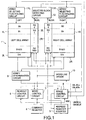
- FIG. 1 is a block diagram of the first preferred embodiment of a batch-erasable NAND type EEPROM (flash memory) according to the present invention.
- a memory cell array 1 is divided into a left cell array 1L and a right cell array 1R.
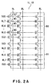
- each of the cell arrays 1L and 1R comprises a HAND cell wherein a plurality of non-volatile memory cells MC are connected in series.
- One end of the NAND cell is connected to a bit line BL via a selecting gate transistor S1 driven by a selecting gate line SGD, and the other end thereof is connected to a common source line via a selecting gate transistor S2 driven by a selecting gate line SGS.
- the range of the NAND cell e.g., the range of eight word lines WL0 through WL7 in the example of FIG. 2A, corresponds to each of blocks B0, B1, ⁇ , each of which serves as a data erase unit.
- each of the cell arrays 1L and 1R comprises 1024 blocks.
- FIG. 2B is a schematic diagram showing a cross section of a non-volatile semiconductor memory device wherein the cell arrays 1L and 1R are formed.
- n-type wells NW1 and NW2 are formed on the surface of a p-type semiconductor substrate SS.
- P-type wells PW1 and PW2 are formed on the surfaces of the n-type wells NW1 and NW2.
- the left cell array 1L is formed on the p-type well W1, and the right cell array 1R is formed on the p-type well PW2.
- the impurity type may be the reverse type thereof.
- the cell arrays 1L and 1R are provided with row decoders 2L and 2R for selectively driving word lines, and sense amplifiers 3L and 3R for sensing read data and latching write data, respectively.
- a command register 4 captures and decodes a command for indicating data readout, writing (program), erase from the outside.
- An address register/counter 5 captures an external address.
- a readout control circuit 6, a write control circuit 7 and an erase control circuit 8 control data readout, writing and erase, respectively, on the basis of the command captured into the command register 4, and the address captured into the address register 5.
- a word line driver 10 supplies a required word line driving voltage to word lines selected by the row decoders 2L and 2R, in accordance with the data readout, writing and erase.
- a boosted writing voltage VP produced by a booster circuit (not shown) is applied to the word lines.
- a boosted erase voltage VE is applied to the p-type wells PW1 and PW2 of the cell array, 0 V is applied to the word lines of the selected block (B1 in the case of FIG. 3), and the word lines of unselected blocks are allowed to be floating.
- the selecting flags LEFT and RIGHT are "L" with respect to the unselected cell arrays by signals UNSELL and UNSELR indicating that the cell arrays, to which the blocks belong, are unselected. Therefore, the signals UNSELL and UNSELR are outputted from the erase control circuit 8 every block.
- the selected block detecting circuit 12 is a circuit for detecting the presence of selection of each of the cell arrays 1L and 1R every block by monitoring common buses BUSL and BUSR provided in the respective cell arrays 1L and 1R.
- each of the common buses BUSL and SUSR is commonly connected to a latch circuit 41 (see FIG. 4) arranged in each block of a corresponding one of the cell arrays 1L and 1R.
- Each of the latch circuits 41 holds block selecting information during data erase. Therefore, the common buses BUSL and BUSR are sense nodes in the selected block retrieval for the verify which will be carried out later, on the basis of the block selecting information for data erase.
- the selected block detecting circuit 12 monitors the common buses BUSL and BUSR during the selected block retrieval after data erase, and outputs signals VBLKLn and VBLKRn indicative of the selected/unselected state of the blocks in the respective cell arrays 1L and 1R. Specifically, when these signals VBLKLn and VBLKRn are "H", these signals indicate that the corresponding blocks are verify disable.
- FIG. 4 shows the construction of a block selecting decoder RDi of each of the row decoders 2L and 2R for selectively driving the word lines.
- a block decoding part 40 carries out a coincidence detection of a row decoder activating signal RDECL/R with a predecode output PREDECi by means of a NAND gate G1 and an inverter I1. If a block is selected, the output of the NAND gate G1 is "L".
- the latch 41 comprising inverters I2a and I2b inversely connected in parallel is an erase flag holding circuit for holding an erase flag indicating that the block is selected during data erase. That is, if an address is inputted from the outside of the chip before erasing the block, the node N1 of the latch 41 is "H" with respect to the selected block, and this is held over the whole period for data erase.
- each of the common buses BUSL and BUSR is commonly provided in each of the cell array regions, and serves as a sense node for detecting whether the block is selected during data erase in the verify operation.
- the common buses BUSL and BUSR are connected to the selected block detecting circuit 12 as shown in FIG. 1.
- the node N1 of the latch 41 is connected to a driving voltage transfer terminal TR via a clocked inverter I11, an inverter I5 and depletion type NMOS transistors QN10 and QN11.
- the output of the inverter I1 is connected to the terminal TR via another clocked inverter I12, the inverter I5 and the transistors QN10 and QN11.
- a transfer switch circuit 42 is operated during data readout and writing (including verify) for transferring a driving voltage (or a power supply voltage) VDREC, which is boosted by a booster circuit (not shown), to the terminal TR. That is, when the block is selected, the output RDECI of the inverter I5 is "H", and this enters a NAND gate G2. A clock signal OSC for charge pump operation enters another input terminal of the NAND gate G2. Therefore, when the block is selected, the clock signal OSC is supplied to the transfer switch circuit 42 via the NAND gate G2. Thus, the transfer switch circuit 42 transfers a voltage VRDEC+ ⁇ ( ⁇ : the threshold voltage of an NMOS transistor QN9) to the terminal TR by the charge pump function.
- the transistor of a word line drive stage 43 is turned on.
- a required driving voltage applied to word line control terminals CG0 through CG7 and selecting gate terminals SGD and SGS is applied to the word lines WL and selecting gate lines SGD1 and SGD2 without decreasing its potential.
- FIG. 5 shows the construction of the selected block detecting circuit 12 shown in FIG. 1.
- the selected block detecting circuit 12 has detecting circuits 12L and 12R having the same construction provided in the cell arrays 1L and 1R, respectively.
- Each of the detecting circuits 12L and 12R has an NMOS transistor QN22 for detecting the presence of discharge of a corresponding one of the common buses BUSL and BUSR of each block of the cell array, and a latch 51 for holding the detected results.
- Each of the detecting circuits 12L and 12R is controlled by timing control signals EBSEN0 and EBSEN2, which are produced from the erase control circuit 8 during data erase to sequentially become "H" every retrieval loop, and by a timing control signal EBSENEn for deactivating the circuit at the final timing every loop.
- the coincidence of the outputs of the two detecting circuits 12L and 12R is detected by a coincidence detecting circuit 12S having a NAND gate G13.
- the retrievals of the erased blocks in the verify operation after data erase are simultaneously carried out in parallel with respect to the left and right cell array 1L and 1R.
- address Ar0, Ar1, ⁇ , Arn of the cell arrays 1L and 1R, "0" and “1" of the most significant address Arn indicate the left and right cell arrays 1L and 1R, and other address Ar0, Ar1, ⁇ , Arn-1 are common to the right and left, so that the retrievals of the erased block the left and right cell arrays 1L and 1R are simultaneously carried out in parallel by the lower address Ar0 through Arn-1 except for the most significant address Arn.
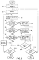
- FIG. 6 is a flow chart showing a data erasing operation in this preferred embodiment.
- This variable BLOCK is a variable used for a verify processing which will be carried out later.
- a usual data erasing operation is carried out (S2). That is, on the basis of an erase command, batch erase is carried out every block selected by an external address.
- S3 a retrieving operation for a verify operation is carried out
- step S6 it is determined whether the left and right cell arrays 1L and 1R have been simultaneously selected. If it is YES, verify readout is carried out simultaneously with respect to the left and right cell arrays 1L and 1R (S9).
- step S10 it is determined whether erase is sufficient. If the determined result of the verify readout is OK, the above described processing from step S11 is carried out. On the other hand, if the determined result is NO, the erase and verify are repeated until it is determined that the number of loops reaches a set number (S13). If the erase is still insufficient after the number of loops reaches the set number, the routine ends as erase failure.
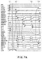
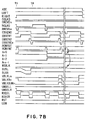
- FIGS. 7A and 7B are timing charts for a data erasing operation of an EEPROM in this preferred embodiment. If a block selecting address to be erased and an erase executing command are inputted, the erase command flag ABE becomes "H", so that an erasing operation is started (t1). That is, the address counter of the block to be erased is initialized by an initializing pulse ROWRST, so that all of the address Ar0, Ar1, ⁇ , Arn become “L”. Simultaneously, an internal signal ECLKO for controlling the erase operation becomes "H" to start the erase operation.
- both of the selecting flags LEFT and RIGHT of the two cell arrays 1L and 1R become "H", so that the two cell arrays are in a selected state during the erase operation.
- the control signal LEN becomes "H”
- the clocked inverter I11 of FIG. 4 is active, so that RDECI becomes "H” with respect to the selected block by the data held by the latch 41.
- a signal BSTON of FIG. 4 is VCC, so that VCC is transferred to the terminal TR via the transistors QN10 and QN11. Therefore, all of the NMOS transistors QN 12 of the word line drive stage 43 are turned on.
- a selected optional number of blocks of the blocks B0 through B1023 of the two cell arrays 1L and 1R are batch-erased.
- a timing signal ERCVEn indicative of the end of the erase operation is produced, so that the erase operation ends (t2).
- an operation for retrieving a block to be erased for verify is carried out.
- the selecting flags LEFT and RIGHT are "H" in the two cell arrays 1L and 1R
- two erased blocks in the left and right cell arrays 1L and 1R having the same address of any one of Ar0 through Arn-1 are simultaneously retrieved in parallel. If one retrieving operation is completed, the address is sequentially incremented by an increment signal ROWINC produced in synchronism with the timing control signal EBSENn.
- both of the output control signals VBLKLn and VBLKRn from the selected block detecting circuit 12 are "H" by the timing control signal EBSEN2, and this is latched by the erase control circuit 8.
- the address is subsequently updated to continue the retrieval without the need of verify. In the example of FIG. 7A, this state is continued until time t2 to t3.
- any one of the control signals UNSELL and UNSELR for deactivating the unselected cell array becomes "H".
- the right cell array 1R is deactivated.
- the control signal VBLKLn indicative of the deactivation of the blocks of the left cell array 1L does not rise, so that the verify operation is carried out in only the left cell array 1L.
- the retrievals are simultaneously carried out in parallel with respect to the left and right cell arrays 1L and 1R selected by the "H" and "L” of the most significant address Arn, and the time required for all of the address Ar0 through Arn-1 to become "H” is the time required to carry out the retrieval, so that the time required to carry out the retrieval is shortened to be half of that in the conventional case.
- the time required to carry out the whole data erase can be shortened.
- the verify operation corresponding thereto is simultaneously carried out. This also shortens the whole erase time.
- the number of the cell arrays has been two.
- the present invention should not be limited thereto. Even if the memory cell array comprises a plurality of optional cell array regions, it is possible to simultaneously retrieve the plurality of cell array regions in parallel by the same technique, and it is possible to obtain the same effects. In particular, as the number of the cell arrays increases, the effect of the shortening of the time required to carry out the retrieval increases.
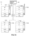
- FIG. 7C shows a case where one memory cell array 110 comprises four cell array regions 110(1) through 110(4).
- the selected block detecting circuit 120 sequentially retrieves whether the blocks B0, B1, ⁇ , B1023 are selected from each of the cell array regions 110(1) through 110(4) during erase. That is, information relating to the erase flag is read out from the latch circuit 41 of each of the row decoders 112(1) through 112(4) at the same timing with respect to the four blocks, to be incorporated into the selected block detecting circuit 120 via the common buses BUS(1) through BUS(4). Then, the selected block detecting circuit 120 identifies whether the block is selected during erase, on the basis of the four erase flags.
- FIG. 8A is a block diagram of the second preferred embodiment of a non-volatile semiconductor memory device according to the present invention. As shown in FIG. 8A, the non-volatile semiconductor memory device in this preferred embodiment has the same structure as that in the above described first preferred embodiment, and has two cell arrays 1L and 1R.
- FIG. 8B is a flow chart showing data erase in the second preferred embodiment.
- the retrieval for the presence of an erased block every array precedes. Then, the retrieval and verify of the selected block are carried out with respect to only a cell array, in which the erase selected block exists, similar to the conventional case, and the operation for retrieving the selected block is not carried out with respect to a cell array, in which the erase selected block does not exist.
- the time required to carry out the retrieving operation is shortened.
- the address of the cell array is updated (S26), and the processing from step S23 is repeated.
- the retrieval whether at least one block selected during the erase operation exists in the cell array is repeated until the retrieval of the final cell array is completed.
- step S24 If it is determined at step S24 that the cell array is selected, the block address BLOCK is initialized (S27), and the block retrieval and verify operation are carried out with respect to the cell array while incrementing the block address. That is, the selected block retrieval is carried out (S28), and it is determined whether the retrieved block is selected to be erased (S29). If it is YES, the verify readout is carried out (S30). If the block is unselected, the block address is updated (S35), and the routine returns to the selected block retrieving step S28. After it is determined that the retrieval of all of the blocks is completed (S34), the routine goes to step S25.
- FIGS. 9A and 9B are timing charts for a data erasing operation in this preferred embodiment.
- the number of cell arrays is two, and ARRAY0 and ARRAY1 correspond to the array selecting flags LEFT and RIGHT in the preceding preferred embodiment, respectively.
- Canon buses BUS0 and BUS1 correspond to the common buses BUSL and BUSR in the preceding preferred embodiment, respectively.
- the construction of a selected block detecting circuit 12 is basically the same as that in the preceding preferred embodiment.
- a timing control signal entering a PMOS transistor QP21 for charging and controlling the common buses BUS0 and BUS1 a timing control signal EBSEN1d rising more lately than the EBSEN0 in the preceding preferred embodiment is used in place of the EBSEN0. Also with respect to other signals, "0" and “1” are used in place of "L” and “R” indicative of the left and right in the preceding preferred embodiment.
- a command flag ABE becomes "H"
- an erasing operation is started (t11).
- the address of a cell array is initialized, and then, two cell arrays are selected to be erased. This erasing operation is the same as that in the preceding preferred embodiment, and all of the selected blocks of the two cell arrays are batch-erased.
- the node N1 of the cell array ARRAY0 is connected to the common bus BUS0.
- This circuit operation is carried out simultaneously with respect to all of the erased blocks in the cell array ARRAY0, and the contents of the erase selecting flag in all of the blocks are batch-outputted to the common bus BUS0 in the form of wired OR.
- the timing control signal EBSEN1d becomes "H".
- the PMOS transistor QP21 for pre-charging the common bus in the erased block selecting circuit 12 shown in FIG. 5 is turned off, so that a block detection is carried out. That is, in the preceding preferred embodiment, the erase selecting flag is detected by the "H" of the timing signal EBSEN0, whereas in this preferred embodiment, the charging PMOS transistor QP21 is lately turned off after the erase selecting flags in the cell array are batch-selected. This is carried out to prevent the potential of the common bus from being decreased by the channel capacities of the transistors QN4 through QN6 of the discharge path 44 of FIG. 4 regardless of no selected block since the erase selecting flags in the cell array are batch-selected.
- the timing control signal EBSEN1d becomes "H” to decrease the potential of the common bus BUS0 so that the erased block exists in the cell array. If it is detected that the erased block exists in the cell array, the erase selected block is retrieved from the cell array. This is the same as the conventional case.
- the block address is incremented to read the selecting flag of the separate block to be erased, and if the common bus BUS0 is discharged, the block is regarded as a selected block.
- the same retrieval and verify operations are carried out.
- the selected block is not detected in the retrieval for the presence of the selected block in the array ARRAY1. Therefore, all of the erase operations end in this time.
- This preferred embodiment is particularly effective when a plurality of erase selecting blocks are not dispersed in a plurality of cell arrays and when the erase selecting blocks are concentrated in a certain cell array. Because the retrieving is not uselessly repeated while updating the address with respect to the cell array having no selected block. Thus, the time required to carry out the erase operation including the verify can be shortened. This effect increases as the number of cell arrays increases.
- the third preferred embodiment substantially uses the same operation flow as that in the second preferred embodiment shown in FIG. 8B, except for a selected block retrieving step S23.
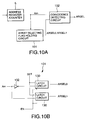
- a block address to be erased is inputted to an address register 5.
- an array selecting flag holding circuit 101 is provided for storing therein an array selecting flag indicative of the presence of an erased block every cell array 1L or 1R when the block address to be erased is inputted.
- FIG. 10B shows an example of the construction of the array selecting flag holding circuit 101 shown in FIG. 10A for use in a non-volatile semiconductor memory device.
- the array selecting flag holding circuit 101 comprises latch circuits 130 and a NOT gate 132.
- the number of latch circuits 130 is the same as that of cell arrays 1L and 1R.
- two latch circuits 130 are provided corresponding to two cell arrays 1L and 1R in FIG.8A.
- the latch circuits 130 corresponding to the cell arrays 1L, 1R store the information that the cell arrays 1L, 1R has been selected, on the basis of the address Arn inputted from the address register/counter 5 at the beginning of the erase operation.
- the address Arn is the most significant address of the address Arn0 through Arn.
- FIG. 10C shows an example of the construction of the latch circuit 130.
- the latch circuit 130 comprises NAND gates 130a through 130c and a NOT gate 130d.
- FIG. 10D shows an example of the construction of the coincidence detecting circuit 102.
- the coincidence detecting circuit 102 comprises a NOT gate 102a and NAND gates 102b through 102d.
- the coincidence detecting circuit 102 compares the address Arn with the array selecting flags ARSEL0, ARSEL1 in retrieving the selected array.
- a set signal SET is HIGH when the address Arn is inputted.
- the information that the cell arrays 1L, 1R have been selected is stored in the latch circuits 130.
- An enable signal EN defines a term during which the latch circuits 130 is in an enabling state.
- the array selecting flags ARSEL0 and ARSEL1 are outputted from the latch circuits 130 and inputted to the coincidence detecting circuit 102.
- the coincidence detecting circuit 102 is inputted the address Arn as well as the array selecting flags ARSEL0 and ARSEL1. In retrieving the selected array, the coincidence detecting circuit 102 compares the address Arn with the array selecting flags ARSEL0 and ARSEL1, and outputs a detecting signal ARSEL when the address Arn corresponding to the cell array including the selected block is inputted.
- the detecting signal ARSEL is inputted to the erase control circuit 8 shown in FIG. 8A.
- the erase selecting flags in the cell array 1L and 1R are not batch-read out, but the address register/counter 5 is sequentially count up the address Arn, and the coincident detecting circuit 102 compares the array selecting flags ARSEL0 and ARSEL1 of the array selecting flag holding circuit 101 with the address Arn. Then, whether or not a cell array includes selected block is determined.
- the sequence of other processes is the same as that in the second embodiment.
- the time required to carry out the erasing operation including the verify can be shortened similar to the second preferred embodiment.
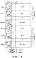
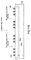
- FIG. 11A shows the constructions of a memory cell array 1 and a row decoder 2.
- FIG. 11B schematically shows a cross section of the memory cell array 1 shown in FIG. 11A.
- the memory cell array 1 is not physically separated by the well.
- an n-type well NW3 is formed on the surface of a p-type semiconductor substrate SS, and a p-type well PW3 is formed on the surface of the n-type well NW3.
- the memory cell array 1 is formed on this single p-type well PW3.
- the memory cell array 1 is divided into a plurality of cell array regions by upper address than a block address. Specifically, an example of a 256 Mb device having address of Ar0 through Ar24 will be described. In this case, the memory cell array 1 can be divided into an upper cell array region 1A and a lower cell array region 1B as shown in FIG. 11A, by the "L" and "H" of the most significant address Ar24 assuming that address Ar14 through Ar24 are block address. Bit lines are continuously provided over all of the blocks in the memory cell array 1.
- common buses BUS0 and BUS1 utilized for simultaneously carrying out block retrievals in parallel with respect to the upper and lower cell array regions 1A and 1B after data erase are provided over all of the blocks of the respective cell array regions 1A and 1B.
- the common buses BUS0 and BUS1 correspond to the common buses BUSL and BUSR provided in the right and left cell array regions in the first preferred embodiment.
- the row decoder 2 basically has the same construction as that in the first preferred embodiment, and is formed as shown in FIG. 4.
- Each of block decode parts RD0, RD1, ⁇ , RD2047 of the row decoder 2 is provided with a latch 41 serving as an erase flag holding circuit, and a discharge path 44 which is controlled by data held by the latch 41, an input block address and a timing signal for selectively discharging the common buses BUS0 and BUS1.
- the detailed constructions thereof are shown in FIG. 4.
- the discharge path 44 is connected to the common bus BUS0 in the upper cell array region 1A, and to the common bus BUS1 in the lower cell array region 1B.
- a selected block detecting circuit 12 is provided in each of the common buses BUS0 and BUS1, similar to the first preferred embodiment.
- the selected block detecting circuit 12 has the same construction as that in FIG. 5.
- the retrieved results are outputted as signals VBLKAn and VBLKBn (corresponding to the VBLKLn and VBLKRn in the first preferred embodiment) indicative of the presence of selected blocks every cell array region.
- data erase can be carried out so as to erase multi-block every block.
- the most significant address is multiple-selected, and Ar24 and its complementary signal Ar24n simultaneously become "H". Therefore, retrievals are simultaneously carried out in parallel every two blocks of each of the cell array regions 1A and 1B selected by the address Ar0 through Ar23.
- the results of the retrieval of blocks are detected and outputted by the selected block detecting circuit 12. On the basis of the output signals VBLKA and VBLKB, erase verify is carried out.
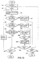
- FIG. 12 is a flow chart specifically showing a data erasing operation in this preferred embodiment. Since the basic operation thereof is the same as that in the first preferred embodiment shown in FIG. 6, different points from FIG. 6 will be described below.
- the steps S4 through S6 of determining the selection of the right and left cell arrays in the first preferred embodiment correspond to steps S4' through S6' of determining the selection of upper and lower cell arrays in this preferred embodiment. If it is determined at step S6' that the upper and lower cell array regions 1A and 1B are simultaneously selected, verify operations can not be simultaneously carried out, so that the verify operations are sequentially carried out one by one, since the upper and lower cell arrays 1A and 1B commonly use bit lines and sense amplifiers.
- the common bus for retrieving blocks is provided in a plurality of cell array regions divided by the address of the memory cell array, the retrievals of blocks can be simultaneously carried out in parallel with respect to the plurality of cell array regions, so that it is possible to accelerate the data erasing operation.
- the present invention should not be limited to the above described preferred embodiments.
- the present invention may not be applied only to NAND type EEPPROMs, but the invention may also be applied to NOR type, DINOR type, AND type and other types of EEPROMs capable of batch-erasing a plurality of erased blocks to be erased.
- an EEPROM capable of shortening the required time to carry out the retrieval of the selected block for the verify operation after data erase and shortening the required time to carry out the whole data erase.
Landscapes
- Engineering & Computer Science (AREA)
- Microelectronics & Electronic Packaging (AREA)
- Read Only Memory (AREA)
Abstract
Description
Claims (17)
- A non-volatile semiconductor memory device comprising:a memory cell array (1) divided into a plurality of cell array regions (1L, 1R), each of which includes a plurality of blocks (B0 through B1023), each of said blocks having electrically rewritable non-volatile memory cells (MC) arranged therein;a data erasing part for selecting one or more of said blocks (B0 through B1023) of said memory cell array (1) to batch-erase data in the selected block(s) as an erased block(s) to be erased;an erase information holding part (41), provided in each of said blocks (B0 through B1023) of said memory cell array (1), for holding erase information indicating that said block is said erased block;a retrieving part (12, BUSL, BUSR) for sequentially reading said erase information, which is held by said erase information holding part (41) in each of said plurality of cell array regions (1L, 1R), every one of said blocks (B0 through B1023) to detect said erased block(s), said retrieving part reading said erase information at the same timing every one of said blocks from each of at least part and each of said plurality of cell array regions (1L, 1R) when said retrieving part reads said erase information from said erase information holding part (41); andan erase verify part (8, 9) for carrying out an erase verify for confirming an erased state of said memory cells (MC) with respect to said erased block(s), which are detected by said retrieving part (12, BUSL, BUSR), said erase verify part repeating a data erase operation with respect to said erased block(s) which are erased insufficiently, and said erase verify part carrying out said erase verify in parallel with respect to said erased block(s) which are detected on the basis of said erase information read at the same timing by said retrieving part (12, BUSL, BUSR).
- A non-volatile semiconductor memory device as set forth in claim 1, wherein said retrieving part (12, BUSL, BUSR) reads said erase information at the same timing every one of said blocks from all of said cell array regions (1L, 1R) included in said memory cell array (1), when said retrieving part reads said erase information from said erase information holding part (41).
- A non-volatile semiconductor memory device as set forth in claim 1, wherein said retrieving part (12, BUSL, BUSR) comprises:common buses (BUSL, BUSR), each of which is provided in each of said cell array regions (1L, 1R) of said memory cell array (1), each of said common buses being connected to said erase information holding part; anda selected block detecting circuit (12), connected to said common buses, for monitoring said common buses to detect whether each of said blocks is a corresponding one of said erased block(s), which are selected during said data erase.
- A non-volatile semiconductor memory device as set forth in claim 3, comprising a discharge path (44) for discharging said common buses with respect to said erased block(s) which are selected during said data erase, when said retrieving part read out said erase information from said erase information holding part (41).
- A non-volatile semiconductor memory device as set forth in claim 1, wherein said plurality of cell array regions of said memory cell array are separated from each other by wells.
- A non-volatile semiconductor memory device as set forth in claim 1, wherein said plurality of cell array regions (1A, 1B) of said memory cell array (1) are formed in a single well and are separated from each other by assigning an address.
- A non-volatile semiconductor memory device comprising:a memory cell array (1) divided into a plurality of cell array regions (1L, 1R), each of which includes a plurality of blocks (B0 through B1023), each of said blocks having electrically rewritable non-volatile memory cells (MC) arranged therein;a data erasing part for selecting one or more of said blocks (B0 through B1023) of said memory cell array (1) to batch-erase data in the selected block(s) as an erased block(s) to be erased;an erase information holding part (41), provided in each of said blocks (B0 through B1023) of said memory cell array (1) for holding erase information indicating that said block is said erased block;a detecting part (12, BUS0, BUS1) for reading said erase information, which is held by said erase information holding part (41) in each of said plurality of cell array regions (1L, 1R), to detect whether said erased block(s) exist in each of said cell array regions; andan erase verify part (8, 9) for carrying out an erase verify for confirming an erased state of said memory cells (MC) with respect to said erased block(s) in said cell array regions, in which the presence of said erased block(s) is detected by said detecting part (12, BUS0, BUS1), said erase verify being carried out with respect to said erased blocks, by sequentially reading said erase information every one of said blocks, and a data erase operation being repeated with respect to said erased block(s) which are erased insufficiently.
- A non-volatile semiconductor memory device as set forth in claim 7, wherein said detecting part (12, BUS0, BUS1) batch-reads said erase information, which is held by said erase information holding part (41) in one of said cell array regions.
- A non-volatile semiconductor memory device as set forth in claim 7, wherein said detecting part (12, BUS0, BUS1) comprises:common buses (BUSL, BUSR), each of which is provided in each of said cell array regions (1L, 1R) of said memory cell array (1), each of said common buses being connected to said erase information holding part; anda selected block detecting circuit (12), connected to said common buses, for monitoring said common buses to detect whether each of said cell array regions (1L, 1R) includes said erased block(s).
- A non-volatile semiconductor memory device as set forth in claim 9, comprising a discharge path (44) for discharging said common buses with respect to said erased block(s) which are selected during said data erase, when said erase information is read out from said erase information holding part (41).
- A non-volatile semiconductor memory device as set forth in claim 9, wherein said plurality of cell array regions of said memory cell array are separated from each other by wells.
- A non-volatile semiconductor memory device comprising:a memory cell array (1) divided into a plurality of cell array regions (1L, 1R), each of which includes a plurality of blocks (B0 through B1023), each of said blocks having electrically rewritable non-volatile memory cells (MC) arranged therein;a data erasing part for selecting one or more of said blocks (B0 through B1023) of said memory cell array (1) to batch-erase data in the selected block(s) as an erased block(s) to be erased;an erase information holding part (101) for holding cell array erase information indicating that each of said cell array regions includes said erased block(s), every one of said cell array regions (1L, 1R);a detecting part (102) for reading said cell array erase information from said erase information holding part (101), to detect whether said erased block(s) exist in each of said cell array regions; andan erase verify part (8, 9) for carrying out an erase verify for confirming an erased state of said memory cells (MC) with respect to said erased block(s) in of said cell array regions, in which the presence of said erased block(s) is detected by said detecting part (12, BUS0, BUS1), said erase verify being carried out with respect to said erased blocks, by sequentially reading said erase information every one of said blocks, and a data erase operation being repeated with respect to said erased block(s) which are erased insufficiently.
- A non-volatile semiconductor memory device as set forth in claim 12, wherein said erase information holding part (101) produces and holds said cell array erase information on the basis of an address inputted to an address register (5) when said data erasing part carries out said data erase.
- A non-volatile semiconductor memory device as set forth in claim 12, wherein said plurality of cell array regions of said memory cell array are separated from each other by wells.
- A data erase controlling method for a non-volatile semiconductor memory device having a memory cell array (1) divided into a plurality of cell array regions (1L, 1R), each of which includes a plurality of blocks (B0 through B1023), each of said blocks having electrically rewritable non-volatile memory cells (MC) arranged therein, said data erase controlling method comprising:a data erasing step of selecting one or more of said blocks (B0 through B1023) of said memory cell array (1) to batch-erase data in the selected block(s) as an erased block(s);an erase information holding step of holding erase information in an erase information holding part (41) provided in each of said blocks (B0 through B1023) of said memory cell array (1), said erase information indicating that said block is said erased block;a retrieving step of sequentially reading said erase information, which is held in said erase information holding part (41) in each of said plurality of cell array regions (1L, 1R), every one of said blocks (B0 through B1023) to detect said erased block(s), said retrieving step reading said erase information at the same timing every one of said blocks from each of at least part and each of said plurality of cell array regions (1L, 1R) when reading said erase information from said erase information holding part (41); andan erase verify step of carrying out an erase verify for confirming an erased state of said memory cells (MC) with respect to said erased block(s), which are detected at said retrieving step, said erase verify step repeating a data erase operation with respect to said erased block(s) which are erased insufficiently, and said erase verify step carrying out said erase verify in parallel with respect to said erased block(s) which are detected on the basis of said erase information read at the same timing by said retrieving step.
- A data erase controlling method for a non-volatile semiconductor memory device having a memory cell array (1) divided into a plurality of cell array regions (1L, 1R), each of which includes a plurality of blocks (B0 through B1023), each of said blocks having electrically rewritable non-volatile memory cells (MC) arranged therein, said data erase controlling method comprising:a data erasing step of selecting one or more of said blocks (B0 through B1023) of said memory cell array (1) to batch-erase data in the selected block(s) as an erased block(s);an erase information holding step of holding erase information in an erase information holding part (41) provided in each of said blocks (B0 through B1023) of said memory cell array (1), said erase information indicating that said block is said erased block;a detecting step of reading said erase information, which is held in said erase information holding part in each of said plurality of cell array regions (1L, 1R), to detect whether said erased block(s) exist in each of said cell array regions; andan erase verify step of carrying out an erase verify for confirming an erased state of said memory cells (MC) with respect to said erased block(s) in said cell array regions, in which the presence of said erased block(s) is detected at said detecting step, said erase verify being carried out with respect to said erased blocks, by sequentially reading said erase information every one of said blocks, and a data erase operation being repeated with respect to said erased block(s) which are erased insufficiently.
- A data erase controlling method for a non-volatile semiconductor memory device having a memory cell array (1) divided into a plurality of cell array regions (1L, 1R), each of which includes a plurality of blocks (B0 through B1023), each of said blocks having electrically rewritable non-volatile memory cells (MC) arranged therein, said data erase controlling method comprising:a data erasing step of selecting one or more of said blocks (B0 through B1023) of said memory cell array (1) to batch-erase data in the selected block(s) as an erased block(s) to be erased;an erase information holding step of holding cell array erase information indicating that each of said cell array regions includes said erased block(s), in an erase information holding part (101) every one of said cell array regions (1L, 1R);a detecting step of reading said cell array erase information from an erase information holding part (101), to detect whether said erased block(s) exist in each of said cell array regions; andan erase verify step of carrying out an erase verify for confirming an erased state of said memory cells (MC) with respect to said erased block(s) in said cell array regions, in which the presence of said erased block(s) is detected at said detecting step, said erase verify step being carried out with respect to said erased blocks, by sequentially reading said erase information every one of said blocks, and a data erase operation being repeated with respect to said erased block(s) which are erased insufficiently.
Applications Claiming Priority (4)
| Application Number | Priority Date | Filing Date | Title |
|---|---|---|---|
| JP9700399 | 1999-04-02 | ||
| JP9700399 | 1999-04-02 | ||
| JP18224899 | 1999-06-28 | ||
| JP18224899A JP3920501B2 (en) | 1999-04-02 | 1999-06-28 | Nonvolatile semiconductor memory device and data erase control method thereof |
Publications (3)
| Publication Number | Publication Date |
|---|---|
| EP1041577A2 true EP1041577A2 (en) | 2000-10-04 |
| EP1041577A3 EP1041577A3 (en) | 2000-10-11 |
| EP1041577B1 EP1041577B1 (en) | 2009-01-14 |
Family
ID=26438141
Family Applications (1)
| Application Number | Title | Priority Date | Filing Date |
|---|---|---|---|
| EP00107016A Expired - Lifetime EP1041577B1 (en) | 1999-04-02 | 2000-03-31 | Non-volatile semiconductor memory device and data erase controlling method for use therein |
Country Status (7)
| Country | Link |
|---|---|
| US (1) | US6512702B1 (en) |
| EP (1) | EP1041577B1 (en) |
| JP (1) | JP3920501B2 (en) |
| KR (1) | KR100344687B1 (en) |
| CN (1) | CN1124618C (en) |
| DE (1) | DE60041376D1 (en) |
| TW (1) | TW444377B (en) |
Cited By (4)
| Publication number | Priority date | Publication date | Assignee | Title |
|---|---|---|---|---|
| FR2820545A1 (en) * | 2001-02-02 | 2002-08-09 | St Microelectronics Sa | METHOD AND DEVICE FOR VERIFYING A GROUP OF NON-VOLATILE MEMORY CELLS |
| US6836863B2 (en) * | 2000-08-11 | 2004-12-28 | Advantest Corporation | Semiconductor memory testing method and apparatus |
| CN100401425C (en) * | 2001-09-28 | 2008-07-09 | 睦塞德技术公司 | Circuit and method for performing variable width searches in content-addressable memory |
| EP2404299A4 (en) * | 2009-03-05 | 2013-03-27 | Mosaid Technologies Inc | Nand flash architecture with multi-level row decoding |
Families Citing this family (55)
| Publication number | Priority date | Publication date | Assignee | Title |
|---|---|---|---|---|
| JP3875570B2 (en) * | 2001-02-20 | 2007-01-31 | 株式会社東芝 | Data writing method for semiconductor memory device and semiconductor memory device |
| CN100481268C (en) * | 2001-06-25 | 2009-04-22 | 旺宏电子股份有限公司 | Erasing method of flash memory |
| JP2003031704A (en) * | 2001-07-17 | 2003-01-31 | Nec Corp | Nonvolatile semiconductor memory device |
| US6614695B2 (en) * | 2001-08-24 | 2003-09-02 | Micron Technology, Inc. | Non-volatile memory with block erase |
| JP2003151285A (en) * | 2001-11-08 | 2003-05-23 | Fujitsu Ltd | Semiconductor memory |
| AU2002217672A1 (en) * | 2001-12-20 | 2002-04-15 | Telefonaktiebolaget Lm Ericsson (Publ) | Penalty free address decoding scheme |
| US6714458B2 (en) * | 2002-02-11 | 2004-03-30 | Micron Technology, Inc. | High voltage positive and negative two-phase discharge system and method for channel erase in flash memory devices |
| CN100421181C (en) * | 2002-07-30 | 2008-09-24 | 希旺科技股份有限公司 | Rewritable non-volatile storage system and its writing method |
| KR100504696B1 (en) * | 2003-02-26 | 2005-08-03 | 삼성전자주식회사 | Nand-type flash memory device having array of status cells for storing block erase/program information |
| JP2005108273A (en) | 2003-09-26 | 2005-04-21 | Toshiba Corp | Nonvolatile semiconductor memory device |
| US6868009B1 (en) * | 2003-10-20 | 2005-03-15 | Macronix International Co., Ltd. | Flash memory device with byte erase |
| JP2005135466A (en) * | 2003-10-29 | 2005-05-26 | Matsushita Electric Ind Co Ltd | Semiconductor memory device |
| US7299314B2 (en) * | 2003-12-31 | 2007-11-20 | Sandisk Corporation | Flash storage system with write/erase abort detection mechanism |
| KR100604561B1 (en) * | 2004-05-11 | 2006-07-31 | 에스티마이크로일렉트로닉스 엔.브이. | NAND flash memory device and well forming method thereof |
| JP2005332148A (en) * | 2004-05-19 | 2005-12-02 | Keihin Corp | Rewritten data rewriting system for in-vehicle control device |
| US7009889B2 (en) | 2004-05-28 | 2006-03-07 | Sandisk Corporation | Comprehensive erase verification for non-volatile memory |
| US7151694B2 (en) * | 2004-06-14 | 2006-12-19 | Macronix International Co., Ltd. | Integrated circuit memory with fast page mode verify |
| US7415646B1 (en) * | 2004-09-22 | 2008-08-19 | Spansion Llc | Page—EXE erase algorithm for flash memory |
| KR100568118B1 (en) | 2004-09-30 | 2006-04-05 | 삼성전자주식회사 | Nonvolatile Memory Device and High Speed Verification Method Therefor |
| KR100648254B1 (en) * | 2004-12-01 | 2006-11-24 | 삼성전자주식회사 | Nonvolatile memory device and its erasing method can reduce erase time |
| JP2006164408A (en) * | 2004-12-08 | 2006-06-22 | Toshiba Corp | Nonvolatile semiconductor memory device and data erasing method thereof. |
| JP4713143B2 (en) * | 2004-12-15 | 2011-06-29 | 富士通セミコンダクター株式会社 | Semiconductor memory device |
| KR100672992B1 (en) | 2005-01-04 | 2007-01-24 | 삼성전자주식회사 | Operation Method of Semiconductor Memory Device |
| CN100464375C (en) * | 2005-10-08 | 2009-02-25 | 晶豪科技股份有限公司 | Erasing method for reducing erasing time and preventing over-erasing |
| US7624239B2 (en) * | 2005-11-14 | 2009-11-24 | Sandisk Corporation | Methods for the management of erase operations in non-volatile memories |
| US7783845B2 (en) * | 2005-11-14 | 2010-08-24 | Sandisk Corporation | Structures for the management of erase operations in non-volatile memories |
| KR100763114B1 (en) * | 2006-05-10 | 2007-10-04 | 주식회사 하이닉스반도체 | Verification method of flash memory device |
| EP1870905B1 (en) * | 2006-06-21 | 2009-12-30 | STMicroelectronics S.r.l. | Method and circuit for electrically programming semiconductor memory cells |
| WO2008010258A1 (en) | 2006-07-18 | 2008-01-24 | Spansion Llc | Nonvolatile storage device and its erase control method |
| CN101115246B (en) * | 2006-07-25 | 2010-06-09 | 中兴通讯股份有限公司 | A kind of data storage method of mobile terminal |
| KR100908526B1 (en) * | 2006-09-29 | 2009-07-20 | 주식회사 하이닉스반도체 | Flash memory device and erase method thereof |
| US7733706B2 (en) | 2006-09-29 | 2010-06-08 | Hynix Semiconductor Inc. | Flash memory device and erase method thereof |
| KR100769771B1 (en) | 2006-09-29 | 2007-10-23 | 주식회사 하이닉스반도체 | Flash memory device and its erasing method |
| JP4908149B2 (en) * | 2006-10-18 | 2012-04-04 | 株式会社東芝 | NAND flash memory |
| US7453734B2 (en) * | 2006-11-01 | 2008-11-18 | Macronix International Co., Ltd. | Method and apparatus for fast programming of memory |
| US7414891B2 (en) * | 2007-01-04 | 2008-08-19 | Atmel Corporation | Erase verify method for NAND-type flash memories |
| JP2008192271A (en) * | 2007-02-08 | 2008-08-21 | Nec Electronics Corp | Semiconductor device and its test method |
| US20080320253A1 (en) * | 2007-06-19 | 2008-12-25 | Andrew Tomlin | Memory device with circuitry for writing data of an atomic transaction |
| US8266391B2 (en) * | 2007-06-19 | 2012-09-11 | SanDisk Technologies, Inc. | Method for writing data of an atomic transaction to a memory device |
| KR20090061344A (en) * | 2007-12-11 | 2009-06-16 | 삼성전자주식회사 | Semiconductor memory device having a mat structure |
| US8775758B2 (en) * | 2007-12-28 | 2014-07-08 | Sandisk Technologies Inc. | Memory device and method for performing a write-abort-safe firmware update |
| JP2008217993A (en) * | 2008-06-19 | 2008-09-18 | Renesas Technology Corp | Nonvolatile semiconductor memory device |
| US8264891B2 (en) | 2008-08-06 | 2012-09-11 | Samsung Electronics Co., Ltd. | Erase method and non-volatile semiconductor memory |
| JP4926144B2 (en) * | 2008-09-09 | 2012-05-09 | ルネサスエレクトロニクス株式会社 | Nonvolatile semiconductor memory device |
| CN102930899B (en) * | 2009-02-11 | 2015-11-25 | 北京兆易创新科技股份有限公司 | A kind of method for deleting of nonvolatile memory and device |
| KR101604631B1 (en) * | 2009-07-21 | 2016-03-18 | 삼성전자주식회사 | Non-volatile memory device and program method thereof |
| CN102609334B (en) * | 2012-01-09 | 2016-05-04 | 晨星软件研发(深圳)有限公司 | Nonvolatile flash memory is wiped abnormal memory block restorative procedure and device |
| JP2015176628A (en) * | 2014-03-17 | 2015-10-05 | 株式会社東芝 | Semiconductor memory device and memory controller |
| CN105892951A (en) * | 2016-04-05 | 2016-08-24 | 柳州定店科技有限公司 | Storage method of memory |
| KR102601213B1 (en) * | 2018-07-03 | 2023-11-10 | 삼성전자주식회사 | Non volatile memory devices and method of fabricating the same |
| US11164638B2 (en) | 2018-07-03 | 2021-11-02 | Samsung Electronics Co., Ltd. | Non-volatile memory device |
| US11631465B2 (en) | 2018-07-03 | 2023-04-18 | Samsung Electronics Co., Ltd. | Non-volatile memory device |
| CN110970075A (en) * | 2019-12-02 | 2020-04-07 | 武汉新芯集成电路制造有限公司 | Storage structure and its erasing method |
| CN110970076B (en) * | 2019-12-02 | 2022-03-18 | 武汉新芯集成电路制造有限公司 | Memory structure and erasing method thereof |
| JP7461868B2 (en) * | 2020-12-25 | 2024-04-04 | ルネサスエレクトロニクス株式会社 | Semiconductor device and control method thereof |
Family Cites Families (7)
| Publication number | Priority date | Publication date | Assignee | Title |
|---|---|---|---|---|
| US5047981A (en) | 1988-07-15 | 1991-09-10 | Texas Instruments Incorporated | Bit and block erasing of an electrically erasable and programmable read-only memory array |
| KR960002006B1 (en) | 1991-03-12 | 1996-02-09 | 가부시끼가이샤 도시바 | Electrically Erasable and Programmable Nonvolatile Memory Device with Write Verification Controller Using Two Reference Levels |
| US5361227A (en) * | 1991-12-19 | 1994-11-01 | Kabushiki Kaisha Toshiba | Non-volatile semiconductor memory device and memory system using the same |
| DE69326370T2 (en) | 1992-03-05 | 2000-01-20 | Kabushiki Kaisha Toshiba, Kawasaki | Non-volatile semiconductor memory device |
| JPH07201191A (en) | 1993-12-28 | 1995-08-04 | Toshiba Corp | Nonvolatile semiconductor memory device |
| KR970005644B1 (en) * | 1994-09-03 | 1997-04-18 | 삼성전자 주식회사 | Multi-block erase and verify device and method of non-volatile semiconductor memory device |
| JPH11177071A (en) * | 1997-12-11 | 1999-07-02 | Toshiba Corp | Nonvolatile semiconductor memory device |
-
1999
- 1999-06-28 JP JP18224899A patent/JP3920501B2/en not_active Expired - Fee Related
-
2000
- 2000-03-30 US US09/539,212 patent/US6512702B1/en not_active Expired - Fee Related
- 2000-03-31 EP EP00107016A patent/EP1041577B1/en not_active Expired - Lifetime
- 2000-03-31 CN CN00108883A patent/CN1124618C/en not_active Expired - Fee Related
- 2000-03-31 DE DE60041376T patent/DE60041376D1/en not_active Expired - Fee Related
- 2000-04-01 TW TW089106150A patent/TW444377B/en not_active IP Right Cessation
- 2000-04-01 KR KR1020000017140A patent/KR100344687B1/en not_active Expired - Fee Related
Cited By (6)
| Publication number | Priority date | Publication date | Assignee | Title |
|---|---|---|---|---|
| US6836863B2 (en) * | 2000-08-11 | 2004-12-28 | Advantest Corporation | Semiconductor memory testing method and apparatus |
| FR2820545A1 (en) * | 2001-02-02 | 2002-08-09 | St Microelectronics Sa | METHOD AND DEVICE FOR VERIFYING A GROUP OF NON-VOLATILE MEMORY CELLS |
| WO2002063632A1 (en) * | 2001-02-02 | 2002-08-15 | Stmicroelectronics Sa | Method and device for verifying a group of non-volatile memory cells |
| CN100401425C (en) * | 2001-09-28 | 2008-07-09 | 睦塞德技术公司 | Circuit and method for performing variable width searches in content-addressable memory |
| EP2404299A4 (en) * | 2009-03-05 | 2013-03-27 | Mosaid Technologies Inc | Nand flash architecture with multi-level row decoding |
| US8854884B2 (en) | 2009-03-05 | 2014-10-07 | Conversant Intellectual Property Management Inc. | NAND flash architecture with multi-level row decoding |
Also Published As
| Publication number | Publication date |
|---|---|
| CN1124618C (en) | 2003-10-15 |
| JP3920501B2 (en) | 2007-05-30 |
| CN1270394A (en) | 2000-10-18 |
| KR100344687B1 (en) | 2002-07-25 |
| US6512702B1 (en) | 2003-01-28 |
| TW444377B (en) | 2001-07-01 |
| EP1041577B1 (en) | 2009-01-14 |
| KR20010066757A (en) | 2001-07-11 |
| EP1041577A3 (en) | 2000-10-11 |
| DE60041376D1 (en) | 2009-03-05 |
| JP2000348492A (en) | 2000-12-15 |
Similar Documents
| Publication | Publication Date | Title |
|---|---|---|
| EP1041577B1 (en) | Non-volatile semiconductor memory device and data erase controlling method for use therein | |
| US6031760A (en) | Semiconductor memory device and method of programming the same | |
| KR100332001B1 (en) | Semiconductor nonvolatile memory device | |
| US6937524B2 (en) | Nonvolatile semiconductor memory device having a write control circuit | |
| JP3898349B2 (en) | Semiconductor memory device | |
| US6865112B2 (en) | Non-volatile semiconductor memory device in which one page is set for a plurality of memory cell arrays | |
| US20010048615A1 (en) | Electrically erasable and programmable non-volatile semiconductor memory with automatic write-verify controller | |
| US8605512B2 (en) | Nonvolatile semiconductor memory device and method of operating a nonvolatile memory device | |
| JPH0628899A (en) | Nonvolatile semiconductor memory device | |
| US7184307B2 (en) | Flash memory device capable of preventing program disturbance according to partial programming | |
| US10641825B2 (en) | Semiconductor storage device, operating method thereof and analysis system | |
| US20170243656A1 (en) | Flash memory device and erase method thereof | |
| JPH10241378A (en) | Semiconductor storage device | |
| JPH113594A (en) | Nonvolatile memory and data writing / reading method | |
| US7248503B2 (en) | Semiconductor nonvolatile storage device | |
| JP2000048582A (en) | Semiconductor storage device | |
| EP0642135B1 (en) | A nonvolatile semiconductor memory and its test method | |
| JP3862092B2 (en) | Nonvolatile memory device | |
| JP3722372B2 (en) | System and device having nonvolatile memory | |
| JP3544222B2 (en) | Nonvolatile semiconductor memory device | |
| KR0176312B1 (en) | Information processing system using semiconductor integrated circuit device | |
| JP2001093291A (en) | Nonvolatile semiconductor memory device | |
| JPH11283399A (en) | Nonvolatile semiconductor memory device and test method therefor | |
| JPH11297100A (en) | Nonvolatile semiconductor memory device and test method therefor |
Legal Events
| Date | Code | Title | Description |
|---|---|---|---|
| PUAI | Public reference made under article 153(3) epc to a published international application that has entered the european phase |
Free format text: ORIGINAL CODE: 0009012 |
|
| PUAL | Search report despatched |
Free format text: ORIGINAL CODE: 0009013 |
|
| 17P | Request for examination filed |
Effective date: 20000405 |
|
| AK | Designated contracting states |
Kind code of ref document: A2 Designated state(s): DE FR GB |
|
| AX | Request for extension of the european patent |
Free format text: AL;LT;LV;MK;RO;SI |
|
| AK | Designated contracting states |
Kind code of ref document: A3 Designated state(s): AT BE CH CY DE DK ES FI FR GB GR IE IT LI LU MC NL PT SE |
|
| AX | Request for extension of the european patent |
Free format text: AL;LT;LV;MK;RO;SI |
|
| AKX | Designation fees paid |
Free format text: DE FR GB |
|
| 17Q | First examination report despatched |
Effective date: 20061023 |
|
| GRAP | Despatch of communication of intention to grant a patent |
Free format text: ORIGINAL CODE: EPIDOSNIGR1 |
|
| GRAS | Grant fee paid |
Free format text: ORIGINAL CODE: EPIDOSNIGR3 |
|
| GRAS | Grant fee paid |
Free format text: ORIGINAL CODE: EPIDOSNIGR3 |
|
| GRAA | (expected) grant |
Free format text: ORIGINAL CODE: 0009210 |
|
| AK | Designated contracting states |
Kind code of ref document: B1 Designated state(s): DE FR GB |
|
| REG | Reference to a national code |
Ref country code: GB Ref legal event code: FG4D |
|
| REF | Corresponds to: |
Ref document number: 60041376 Country of ref document: DE Date of ref document: 20090305 Kind code of ref document: P |
|
| PGFP | Annual fee paid to national office [announced via postgrant information from national office to epo] |
Ref country code: GB Payment date: 20090325 Year of fee payment: 10 |
|
| PGFP | Annual fee paid to national office [announced via postgrant information from national office to epo] |
Ref country code: DE Payment date: 20090327 Year of fee payment: 10 |
|
| PGFP | Annual fee paid to national office [announced via postgrant information from national office to epo] |
Ref country code: FR Payment date: 20090316 Year of fee payment: 10 |
|
| PLBE | No opposition filed within time limit |
Free format text: ORIGINAL CODE: 0009261 |
|
| STAA | Information on the status of an ep patent application or granted ep patent |
Free format text: STATUS: NO OPPOSITION FILED WITHIN TIME LIMIT |
|
| 26N | No opposition filed |
Effective date: 20091015 |
|
| GBPC | Gb: european patent ceased through non-payment of renewal fee |
Effective date: 20100331 |
|
| REG | Reference to a national code |
Ref country code: FR Ref legal event code: ST Effective date: 20101130 |
|
| PG25 | Lapsed in a contracting state [announced via postgrant information from national office to epo] |
Ref country code: FR Free format text: LAPSE BECAUSE OF NON-PAYMENT OF DUE FEES Effective date: 20100331 |
|
| PG25 | Lapsed in a contracting state [announced via postgrant information from national office to epo] |
Ref country code: DE Free format text: LAPSE BECAUSE OF NON-PAYMENT OF DUE FEES Effective date: 20101001 |
|
| PG25 | Lapsed in a contracting state [announced via postgrant information from national office to epo] |
Ref country code: GB Free format text: LAPSE BECAUSE OF NON-PAYMENT OF DUE FEES Effective date: 20100331 |