EP1041440A2 - System and method for reducing corner rounding in mask fabrication - Google Patents
System and method for reducing corner rounding in mask fabrication Download PDFInfo
- Publication number
- EP1041440A2 EP1041440A2 EP00104732A EP00104732A EP1041440A2 EP 1041440 A2 EP1041440 A2 EP 1041440A2 EP 00104732 A EP00104732 A EP 00104732A EP 00104732 A EP00104732 A EP 00104732A EP 1041440 A2 EP1041440 A2 EP 1041440A2
- Authority
- EP
- European Patent Office
- Prior art keywords
- mask blank
- recited
- energy beam
- pattern
- positioning
- Prior art date
- Legal status (The legal status is an assumption and is not a legal conclusion. Google has not performed a legal analysis and makes no representation as to the accuracy of the status listed.)
- Granted
Links
Images



Classifications
-
- G—PHYSICS
- G03—PHOTOGRAPHY; CINEMATOGRAPHY; ANALOGOUS TECHNIQUES USING WAVES OTHER THAN OPTICAL WAVES; ELECTROGRAPHY; HOLOGRAPHY
- G03F—PHOTOMECHANICAL PRODUCTION OF TEXTURED OR PATTERNED SURFACES, e.g. FOR PRINTING, FOR PROCESSING OF SEMICONDUCTOR DEVICES; MATERIALS THEREFOR; ORIGINALS THEREFOR; APPARATUS SPECIALLY ADAPTED THEREFOR
- G03F1/00—Originals for photomechanical production of textured or patterned surfaces, e.g., masks, photo-masks, reticles; Mask blanks or pellicles therefor; Containers specially adapted therefor; Preparation thereof
- G03F1/68—Preparation processes not covered by groups G03F1/20 - G03F1/50
- G03F1/76—Patterning of masks by imaging
- G03F1/78—Patterning of masks by imaging by charged particle beam [CPB], e.g. electron beam patterning of masks
-
- H—ELECTRICITY
- H10—SEMICONDUCTOR DEVICES; ELECTRIC SOLID-STATE DEVICES NOT OTHERWISE PROVIDED FOR
- H10P—GENERIC PROCESSES OR APPARATUS FOR THE MANUFACTURE OR TREATMENT OF DEVICES COVERED BY CLASS H10
- H10P76/00—Manufacture or treatment of masks on semiconductor bodies, e.g. by lithography or photolithography
Definitions
- This disclosure relates to semiconductor fabrication tools and more particularly, to an improved system and method for generating patterns on reticles used in semiconductor fabrication processes.
- Semiconductor fabrication processes typically include photolithographic processing to pattern areas of a surface of a semiconductor device.
- the semiconductor fabrication process typically includes applying a photoresist material to the surface of the semiconductor device.
- the photoresist is patterned by exposing the photoresist to light, typically ultraviolet light, to crosslink the resist material (negative resist). This cross linking prevents a reaction with a developer which develops away areas of the photoresist which were not crosslinked by the exposure to the UV light.
- Other types of photoresists have chains broken by exposure (positive resist) to ultraviolet light.
- Photoresists are patterned using a photomask.
- the photomask functions as a shield to prevent light form passing through it in predetermined areas during photolithography.
- the photomask typically provides a black or highly absorbent layer of material, usually chromium or a chromium alloy, patterned in accordance with the patterning design to be projected onto the photoresist.
- the absorbent layer is formed on a substrate, which may include a glass or quartz material.
- Other techniques are used which may include electrons and electron beam masks, scattering masks and/or stencil masks, for example, scattering with angular limitation in projection electron beam lithography (SCALPEL).
- Reticles may be written by laser pattern generators or electron beam pattern generators. Since reticles typically include a multitude of features below a micron in size. Fabrication is performed using automated devices. Referring to FIG. 1, a reticle fabrication device 10 is shown. Device 10 includes a stage 14 for positioning a mask or reticle 16 to be fabricated. An energy source 18 provides a laser beam or an electron beam for writing a pattern on mask 16 with a predetermined intensity of light or electrons. Mask 16 is preferably guided by stage 14 according to a computer generated image of the pattern to be written on mask 16.
- Both laser and electron beam pattern generators have the capability for complex reticle patterns, including those with narrow geometries, dense optical proximity correction (OPC) and phase shift masks (PSM).
- OPC dense optical proximity correction
- PSM phase shift masks
- OPC helps compensate for lost light to ensure that the precise patterns are formed on a semiconductor wafer. For example, without OPC, a rectangle can end up looking like an oval on the wafer because light tends to round on the edges. OPC corrects this by adding tiny serifs (lines) to the corner to ensure that the corners are not rounded or moving a feature edge so wafer features are sized more accurately.
- Phase shift masks alter the phase of light passing through the photomask, and permit improved depth of focus and resolution on the wafer. Phase-shift helps reduce distortion on line resolution of wafer surface irregularities.
- a circular laser/electron beam spot 30 is shown for writing a pattern on for a reticle on a mask blank 32.
- Mask blank 32 includes a resist layer 33 formed on a blank mask 32.
- a pattern 34 is formed by exposing portions of resist to light or electrons. The pattern is created by applying laser/electron spot 30 thereon to expose resist 33.
- blank mask 32 includes an energy absorbent material, such as, chromium, molybdenum or their alloys, or metal oxides on a glass or quartz substrate. After exposure resist 33 is developed and exposed portions of energy absorbent material on blank mask 32 is etched away.
- corner rounding As laser/electron spot 30 approaches a corner 38, resist 33 cannot be exposed in corner 38 as a result of the geometry of laser/electron spot 30. This is referred to as corner rounding.
- the large corner radius is related to the beam diameter as approximately equal to 1.17 ⁇ beam diameter for laser beams.
- State of the art tools are capable of corner rounding as low as 300 nm.
- a method for fabricating mask patterns in accordance with the present invention includes the steps of providing a mask blank for patterning, propagating an energy beam having an elliptical cross-sectional shape onto the mask blank, the elliptical cross-sectional shape having an elongated axis and edges at opposite ends of the elongated axis and positioning the mask blank to write a pattern on the mask blank wherein the positioning includes employing the edges of the elliptical cross-sectional shape of the energy beam to write corners of the pattern.
- Another method for fabricating mask patterns for processing semiconductor devices comprising the steps of providing a mask blank to be patterned, providing a design data set for a pattern to be written on the mask blank, propagating an energy beam having an elliptical cross-sectional shape onto the mask blank, the elliptical cross-sectional shape having an elongated axis and edges at opposite ends of the elongated axis and translating and rotating the mask blank according to the design data set to write a pattern on the mask blank wherein the rotating includes employing the edges of the elliptical cross-sectional shape of the energy beam to write corners of the pattern.
- the step of positioning may include the steps of mounting the mask blank on a positioner for positioning the mask blank.
- the step of propagating a energy beam may include the step of shaping the beam using a lens system.
- the step of propagating an energy beam may include the step of propagating an ultraviolet laser beam.
- the step of propagating an energy beam may include the step of propagating an electron beam.
- the step of positioning the mask blank preferably includes the step of writing corners by positioning the elongated axis of the energy beam at an angle that bisects an angle formed by adjacent sides of the corners.
- a system for fabricating mask patterns in accordance with the present invention includes an energy source for providing an elliptical cross-sectional shape onto a mask blank, the elliptical cross-sectional shape having an elongated axis and edges at opposite ends of the elongated axis and a positioner for positioning the mask blank to write a pattern on the mask blank such that the edges of the elliptical cross-sectional shape of an energy beam are employed to write corners of the pattern.
- the system may further include a processor for providing control signals to the positioner for positioning the mask blank.
- the processor preferably includes a memory storage device, the memory storage device including a data set for providing digital data representing the pattern to the processor for producing the control signals.
- the energy beam is preferably shaped using a lens system.
- the energy beam preferably includes an ultraviolet laser beam or an electron beam having energies of about 50 keV or less.
- This disclosure relates to semiconductor fabrication tools and more particularly, to an improved system and method for generating patterns on reticles used in semiconductor fabrication processes.
- the present invention provides an elliptical beam which advantageously provides for smaller corner rounding when writing edges on a reticle used for semiconductor fabrication. Better accuracy writing is provided by manipulating the placement of the elliptical laser spot according to a special corner writing method which is preferably computer controlled.
- the special corner rounding method and the elliptically shaped laser/electron spot reduces the need for the use of add-on structures such as serifs, hammerheads, etc.
- Mask 102 begins the process as a blank, that is, no pattern exists thereon.
- Blank Mask 102 includes an energy absorbent material, such as, chromium, molybdenum or their alloys, or metal oxides on a glass or quartz substrate.
- Mask 102 is mounted to a stage or positioner 106 or equivalent positioning device .
- Stage 106 is capable of accurately positioning mask 102 including rotations.
- a lens system 104 is included for focusing a laser/electron beam 112 generated by an energy source 110.
- Energy source 110 preferably generates light in the ultraviolet wavelengths or an electron beam with electrons having energies of about 50 keV or less.
- Energy source 110 may be, for example, an excimer laser.
- Lens system 104 controls the size and shape of a spot used to write a pattern on mask 102.
- an elliptically shaped laser/electron spot is provided using lens system 104.
- Ellipticity of the beam may be created and controlled by the astigmatism of lens system 104, thereby varying dimensions A and B as shown in FIG. 4.
- source 110 During fabrication, source 110 generates beam 112. Beam 112 is focused and shaped by lens system 104 which directs beam 112 onto mask 102. Mask 102 is manipulated by translating and rotating stage 106 according to a pattern which is preferably stored in memory 114 of a processor 108. Processor sends signals to control the stage's motion to write the pattern stored in memory 114 on a resist layer. Source 110 is also preferably controlled by processor 108. Processor 108 sends signals to source 110 to turn beam 112 on and off in accordance with the pattern. Alternately, a shutter 116 may be used to halt the propagation of laser beam 112.
- vibration isolation systems may be used to isolate environmental vibration from impacting the writing process.
- Environmental conditions such as ambient gases and gas flow in the vicinity of mask 102 may be provided and controlled.
- other embodiments of the present invention may maintain mask 102 stationary while manipulating source 110 by, for example, using mirrors or other suitable devices to deflect and control beam 112 position relative to mask 102.
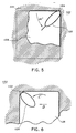
- an elliptical laser/electron spot 120 is shown for writing a pattern 128 on a mask 122 or reticle in accordance with the present invention.
- a corner radius 124 is reduced over conventional circular spots.
- Spot 120 may be positioned to have the elongated axis bisect the corner to be written.
- spot 120 is angled at about 45 degrees to write perpendicular corners of the pattern on mask 122. In this way, corner rounding is minimized for corner radius 124.
- the present invention provides a rotating stage 106 (FIG. 3) to provide for both the rotation an translation of spot 120.
- Spot 120 is employed to expose a resist layer 121 for forming pattern 128 by subsequent development and etching of mask 122.
- elliptical spot 120 is translated in the direction of arrow "D" and rotated in the direction of arrow "C".
- an opposite corner radius 130 may be written with the same reduction in corner rounding as for corner radius 124.
- Other configurations and geometries may also be written using similar techniques.
- a block/flow diagram for generating pattern in accordance with the present invention is illustratively shown.
- a system such as system 100, is provided for fabricating masks or reticles in accordance with the invention.
- a blank mask is provided onto which a pattern is to be formed.
- the blank may include a glass, quartz or equivalent substrate having an energy absorbent layer formed thereon.
- a resist layer is formed on the blank for processing as follows.
- a design pattern is preferably provided in the form of digital data to a processor which converts the data to a set of instructions for a stage on which a blank reticle or mask is mounted for patterning.
- an elliptical beam is provided to write a pattern on the mask.
- the beam applies energy in the form of a laser or electron beam to pattern the resist.
- the stage translates and rotates the mask in the presence of the elliptical laser beam in accordance with the instruction set provided by the processor.
- the processor may include software which includes predetermined laser/electron spot positioning schemes which align the elliptical spot with the corners to be written. In this way, the spot achieves the reduced corner rounding as described above.
- the method continues in block 210 until the mask blank has been completely patterned according to the design data.
- the patterned resist on the mask is developed, and the remaining resist protects areas of the energy absorbent material on the substrate of the mask.
- An additional etching step is performed in block 214 to remove portions of the energy absorbent material in accordance with the resist pattern to form the mask.
- the present invention advantageously, achieves corner radius reduction without an increase in data volume of the design data since reliance on add-on structures such as serifs and hammerheads is reduced.
- add-on structures such as serifs and hammerheads
- the present invention may use the elliptical cross-sectional beam in conjunction with a circular cross-sectional beam.
- the circular beam may be used to perform bulk patterning operations while the elliptical beam may be used to write corners in the pattern.
- the same source may also be used for the beam while the shape form circular to elliptical (or vice versa) is performed by changing or modifying the lens system used.
Landscapes
- Physics & Mathematics (AREA)
- Engineering & Computer Science (AREA)
- Plasma & Fusion (AREA)
- General Physics & Mathematics (AREA)
- Preparing Plates And Mask In Photomechanical Process (AREA)
- Exposure And Positioning Against Photoresist Photosensitive Materials (AREA)
- Electron Beam Exposure (AREA)
- Exposure Of Semiconductors, Excluding Electron Or Ion Beam Exposure (AREA)
Abstract
Description
Claims (21)
- A method for fabricating mask patterns comprising the steps of:providing a mask blank for patterning;propagating an energy beam having an elliptical cross-sectional shape onto the mask blank, the elliptical cross-sectional shape having an elongated axis and edges at opposite ends of the elongated axis; andpositioning the mask blank to write a pattern on the mask blank wherein the positioning includes employing the edges of the elliptical cross-sectional shape of the energy beam to write corners of the pattern.
- The method as recited in claim 1, wherein the step of positioning includes the steps of mounting the mask blank on a positioner for positioning the mask blank.
- The method as recited in claim 1, wherein the step of propagating an energy beam includes the step of shaping the energy beam using a lens system.
- The method as recited in claim 1, wherein the step of propagating an energy beam includes the step of propagating an ultraviolet laser beam.
- The method as recited in claim 1, wherein the step of positioning the mask blank includes the step of writing corners by positioning the elongated axis of the elliptical cross-sectional shape of the energy beam at an angle that bisects an angle formed by adjacent sides of the corners.
- The method as recited in claim 1, wherein the step of propagating an energy beam includes the step of propagating an electron beam.
- The method as recited in claim 6, wherein the electron beam includes electrons with energies of about 50,000 eV or less.
- A method for fabricating mask patterns for processing semiconductor devices comprising the steps of:providing a mask blank to be patterned;providing a design data set for a pattern to be written on the mask blank;propagating an energy beam having an elliptical cross-sectional shape onto the mask blank, the elliptical cross-sectional shape having an elongated axis and edges at opposite ends of the elongated axis; andtranslating and rotating the mask blank according to the design data set to write a pattern on the mask blank wherein the rotating includes employing the edges of the elliptical cross-sectional shape of the energy beam to write corners of the pattern.
- The method as recited in claim 8, wherein the step of positioning includes the steps of mounting the mask blank on a positioner for positioning the mask blank.
- The method as recited in claim 9, wherein the step of propagating an energy beam includes the step of shaping the energy beam using a lens system.
- The method as recited in claim 9, wherein the step of propagating an energy beam includes the step of propagating an ultraviolet laser beam.
- The method as recited in claim 9, wherein the step of positioning the mask blank includes the step of writing corners by positioning the elongated axis of the energy beam at an angle that bisects an angle formed by adjacent sides of the corners.
- The method as recited in claim 8, wherein the step of propagating an energy beam includes the step of propagating an electron beam.
- The method as recited in claim 13, wherein the electron beam includes electrons with energies of about 50,000 eV or less.
- A system for fabricating mask patterns comprising:an energy source for providing an elliptical cross-sectional shape onto a mask blank, the elliptical cross-sectional shape having an elongated axis and edges at opposite ends of the elongated axis; anda positioner for positioning the mask blank to write a pattern on the mask blank such that the edges of the elliptical cross-sectional shape of an energy beam are employed to write corners of the pattern.
- The system as recited in claim 15, further comprises a processor for providing control signals to the positioner for positioning the mask blank.
- The system as recited in claim 16, wherein the processor includes a memory storage device, the memory storage device including a data set for providing digital data representing the pattern to the processor for producing the control signals.
- The system as recited in claim 15, wherein the energy beam is shaped using a lens system.
- The system as recited in claim 15, wherein the energy beam includes an ultraviolet laser beam.
- The system as recited in claim 15, wherein the energy beam includes an electron beam.
- The system as recited in claim 20, wherein the electron beam includes electrons with energies of about 50,000 eV or less.
Applications Claiming Priority (2)
| Application Number | Priority Date | Filing Date | Title |
|---|---|---|---|
| US280615 | 1999-03-29 | ||
| US09/280,615 US6214496B1 (en) | 1999-03-29 | 1999-03-29 | Method for reducing corner rounding in mask fabrication utilizing elliptical energy beam |
Publications (3)
| Publication Number | Publication Date |
|---|---|
| EP1041440A2 true EP1041440A2 (en) | 2000-10-04 |
| EP1041440A3 EP1041440A3 (en) | 2002-01-02 |
| EP1041440B1 EP1041440B1 (en) | 2006-03-01 |
Family
ID=23073859
Family Applications (1)
| Application Number | Title | Priority Date | Filing Date |
|---|---|---|---|
| EP00104732A Expired - Lifetime EP1041440B1 (en) | 1999-03-29 | 2000-03-04 | System and method for reducing corner rounding in mask fabrication |
Country Status (7)
| Country | Link |
|---|---|
| US (1) | US6214496B1 (en) |
| EP (1) | EP1041440B1 (en) |
| JP (1) | JP2000310845A (en) |
| KR (1) | KR100417904B1 (en) |
| CN (1) | CN1204455C (en) |
| DE (1) | DE60026187T2 (en) |
| TW (1) | TW479273B (en) |
Families Citing this family (5)
| Publication number | Priority date | Publication date | Assignee | Title |
|---|---|---|---|---|
| US6767674B2 (en) * | 2001-10-26 | 2004-07-27 | Infineon Technologies Ag | Method for obtaining elliptical and rounded shapes using beam shaping |
| US7405147B2 (en) | 2004-01-30 | 2008-07-29 | International Business Machines Corporation | Device and methodology for reducing effective dielectric constant in semiconductor devices |
| US7244953B2 (en) * | 2005-10-03 | 2007-07-17 | Applied Materials, Inc. | Beam exposure writing strategy system and method |
| JP4922718B2 (en) * | 2006-10-04 | 2012-04-25 | 株式会社日立ハイテクノロジーズ | Insulating film dry etching method |
| KR102688569B1 (en) | 2018-12-13 | 2024-07-25 | 삼성전자주식회사 | Design method for mask layout, OPC(Optical Proximity Correction) method, and methods for manufacturing mask using the OPC method |
Family Cites Families (11)
| Publication number | Priority date | Publication date | Assignee | Title |
|---|---|---|---|---|
| JP2734267B2 (en) * | 1991-12-25 | 1998-03-30 | 日本電気株式会社 | Positioning device for mounting optical elements |
| JPH05315224A (en) * | 1992-05-07 | 1993-11-26 | Mitsubishi Electric Corp | Projection exposure device |
| KR0136213B1 (en) * | 1993-08-23 | 1998-04-29 | 마사시 고지마 | Photomask Inspection Method and Apparatus |
| US5494697A (en) * | 1993-11-15 | 1996-02-27 | At&T Corp. | Process for fabricating a device using an ellipsometric technique |
| JP2595885B2 (en) * | 1993-11-18 | 1997-04-02 | 日本電気株式会社 | Semiconductor device and manufacturing method thereof |
| DE69423716T2 (en) * | 1993-12-22 | 2000-08-17 | Canon K.K., Tokio/Tokyo | Imaging device |
| JPH07249591A (en) * | 1994-03-14 | 1995-09-26 | Matsushita Electric Ind Co Ltd | Laser annealing method for semiconductor thin film and thin film semiconductor device |
| JP3627355B2 (en) * | 1996-02-22 | 2005-03-09 | ソニー株式会社 | Scanning exposure equipment |
| JP3512945B2 (en) * | 1996-04-26 | 2004-03-31 | 株式会社東芝 | Pattern forming method and pattern forming apparatus |
| US5847959A (en) * | 1997-01-28 | 1998-12-08 | Etec Systems, Inc. | Method and apparatus for run-time correction of proximity effects in pattern generation |
| JP3892565B2 (en) * | 1997-02-28 | 2007-03-14 | 株式会社東芝 | Pattern formation method |
-
1999
- 1999-03-29 US US09/280,615 patent/US6214496B1/en not_active Expired - Lifetime
-
2000
- 2000-03-04 DE DE60026187T patent/DE60026187T2/en not_active Expired - Lifetime
- 2000-03-04 EP EP00104732A patent/EP1041440B1/en not_active Expired - Lifetime
- 2000-03-15 TW TW089104759A patent/TW479273B/en not_active IP Right Cessation
- 2000-03-29 JP JP2000092102A patent/JP2000310845A/en not_active Withdrawn
- 2000-03-29 KR KR10-2000-0016056A patent/KR100417904B1/en not_active Expired - Fee Related
- 2000-03-29 CN CNB001047981A patent/CN1204455C/en not_active Expired - Fee Related
Also Published As
| Publication number | Publication date |
|---|---|
| KR20000063045A (en) | 2000-10-25 |
| EP1041440B1 (en) | 2006-03-01 |
| US6214496B1 (en) | 2001-04-10 |
| KR100417904B1 (en) | 2004-02-11 |
| EP1041440A3 (en) | 2002-01-02 |
| CN1204455C (en) | 2005-06-01 |
| CN1269529A (en) | 2000-10-11 |
| DE60026187D1 (en) | 2006-04-27 |
| TW479273B (en) | 2002-03-11 |
| JP2000310845A (en) | 2000-11-07 |
| DE60026187T2 (en) | 2006-12-14 |
Similar Documents
| Publication | Publication Date | Title |
|---|---|---|
| US6767674B2 (en) | Method for obtaining elliptical and rounded shapes using beam shaping | |
| US5538833A (en) | High resolution phase edge lithography without the need for a trim mask | |
| TWI327685B (en) | Optical proximity correction using chamfers and rounding at corners | |
| KR100483513B1 (en) | Hybrid phase-shift mask | |
| KR100799527B1 (en) | Methods and Devices for Compound Optical Lithography | |
| TWI422965B (en) | Photomask and its manufacturing method and reticle correction method and corrected reticle | |
| US20020177078A1 (en) | Proximity correction using shape engineering | |
| US6551750B2 (en) | Self-aligned fabrication technique for tri-tone attenuated phase-shifting masks | |
| US20040029024A1 (en) | Exposure method, mask fabrication method, fabrication method of semiconductor device, and exposure apparatus | |
| US6214496B1 (en) | Method for reducing corner rounding in mask fabrication utilizing elliptical energy beam | |
| US7759660B2 (en) | Electron beam lithography system | |
| JP2000284466A (en) | Projection enhancement mask to improve process window | |
| US7018788B2 (en) | Phase shifting lithographic process | |
| JPH05273739A (en) | Pattern transfer method | |
| US11137691B1 (en) | Fixing blank mask defects by revising layouts | |
| HK1031920A (en) | System and method for reducing corner rounding in mask fabrication | |
| US20050130047A1 (en) | Method for printability enhancement of complementary masks | |
| JP2006179938A (en) | Optimization to avoid sidelobe printing | |
| JPH04368947A (en) | Formation of phase shift mask | |
| CN100468013C (en) | Phase-shift photomask and method for improving printability of on-wafer structures | |
| JP3320062B2 (en) | Mask and pattern forming method using the mask | |
| JPH0844039A (en) | Halftone phase shift mask and resist exposure method | |
| US20050053851A1 (en) | Apparatus and method to improve the resolution of photolithography systems by improving the temperature stability of the reticle | |
| JPH08101491A (en) | Photo mask | |
| KR100702792B1 (en) | Exposure apparatus for semiconductor manufacturing |
Legal Events
| Date | Code | Title | Description |
|---|---|---|---|
| PUAI | Public reference made under article 153(3) epc to a published international application that has entered the european phase |
Free format text: ORIGINAL CODE: 0009012 |
|
| AK | Designated contracting states |
Kind code of ref document: A2 Designated state(s): DE FR GB IE IT NL Kind code of ref document: A2 Designated state(s): AT BE CH CY DE DK ES FI FR GB GR IE IT LI LU MC NL PT SE |
|
| AX | Request for extension of the european patent |
Free format text: AL;LT;LV;MK;RO;SI |
|
| PUAL | Search report despatched |
Free format text: ORIGINAL CODE: 0009013 |
|
| AK | Designated contracting states |
Kind code of ref document: A3 Designated state(s): AT BE CH CY DE DK ES FI FR GB GR IE IT LI LU MC NL PT SE |
|
| AX | Request for extension of the european patent |
Free format text: AL;LT;LV;MK;RO;SI |
|
| 17P | Request for examination filed |
Effective date: 20020701 |
|
| AKX | Designation fees paid |
Free format text: DE FR GB IE IT NL |
|
| RAP1 | Party data changed (applicant data changed or rights of an application transferred) |
Owner name: INFINEON TECHNOLOGIES AG |
|
| 17Q | First examination report despatched |
Effective date: 20050107 |
|
| GRAP | Despatch of communication of intention to grant a patent |
Free format text: ORIGINAL CODE: EPIDOSNIGR1 |
|
| GRAS | Grant fee paid |
Free format text: ORIGINAL CODE: EPIDOSNIGR3 |
|
| GRAA | (expected) grant |
Free format text: ORIGINAL CODE: 0009210 |
|
| AK | Designated contracting states |
Kind code of ref document: B1 Designated state(s): DE FR GB IE IT NL |
|
| REG | Reference to a national code |
Ref country code: GB Ref legal event code: FG4D |
|
| PGFP | Annual fee paid to national office [announced via postgrant information from national office to epo] |
Ref country code: NL Payment date: 20060314 Year of fee payment: 7 |
|
| REG | Reference to a national code |
Ref country code: IE Ref legal event code: FG4D |
|
| REF | Corresponds to: |
Ref document number: 60026187 Country of ref document: DE Date of ref document: 20060427 Kind code of ref document: P |
|
| ET | Fr: translation filed | ||
| PLBE | No opposition filed within time limit |
Free format text: ORIGINAL CODE: 0009261 |
|
| STAA | Information on the status of an ep patent application or granted ep patent |
Free format text: STATUS: NO OPPOSITION FILED WITHIN TIME LIMIT |
|
| 26N | No opposition filed |
Effective date: 20061204 |
|
| PGFP | Annual fee paid to national office [announced via postgrant information from national office to epo] |
Ref country code: GB Payment date: 20070322 Year of fee payment: 8 |
|
| NLV4 | Nl: lapsed or anulled due to non-payment of the annual fee |
Effective date: 20071001 |
|
| PG25 | Lapsed in a contracting state [announced via postgrant information from national office to epo] |
Ref country code: NL Free format text: LAPSE BECAUSE OF NON-PAYMENT OF DUE FEES Effective date: 20071001 |
|
| GBPC | Gb: european patent ceased through non-payment of renewal fee |
Effective date: 20080304 |
|
| PG25 | Lapsed in a contracting state [announced via postgrant information from national office to epo] |
Ref country code: GB Free format text: LAPSE BECAUSE OF NON-PAYMENT OF DUE FEES Effective date: 20080304 |
|
| REG | Reference to a national code |
Ref country code: FR Ref legal event code: TP Owner name: QIMONDA AG,, DE Effective date: 20120123 |
|
| REG | Reference to a national code |
Ref country code: FR Ref legal event code: PLFP Year of fee payment: 16 |
|
| PGFP | Annual fee paid to national office [announced via postgrant information from national office to epo] |
Ref country code: IE Payment date: 20150326 Year of fee payment: 16 |
|
| PGFP | Annual fee paid to national office [announced via postgrant information from national office to epo] |
Ref country code: FR Payment date: 20150319 Year of fee payment: 16 |
|
| REG | Reference to a national code |
Ref country code: DE Ref legal event code: R081 Ref document number: 60026187 Country of ref document: DE Owner name: INFINEON TECHNOLOGIES AG, DE Free format text: FORMER OWNER: QIMONDA AG, 81739 MUENCHEN, DE Ref country code: DE Ref legal event code: R081 Ref document number: 60026187 Country of ref document: DE Owner name: POLARIS INNOVATIONS LTD., IE Free format text: FORMER OWNER: QIMONDA AG, 81739 MUENCHEN, DE |
|
| PGFP | Annual fee paid to national office [announced via postgrant information from national office to epo] |
Ref country code: IT Payment date: 20150330 Year of fee payment: 16 |
|
| REG | Reference to a national code |
Ref country code: DE Ref legal event code: R081 Ref document number: 60026187 Country of ref document: DE Owner name: POLARIS INNOVATIONS LTD., IE Free format text: FORMER OWNER: INFINEON TECHNOLOGIES AG, 85579 NEUBIBERG, DE |
|
| PGFP | Annual fee paid to national office [announced via postgrant information from national office to epo] |
Ref country code: DE Payment date: 20150818 Year of fee payment: 16 |
|
| REG | Reference to a national code |
Ref country code: FR Ref legal event code: TP Owner name: INFINEON TECHNOLOGIES AG, DE Effective date: 20160212 |
|
| REG | Reference to a national code |
Ref country code: DE Ref legal event code: R119 Ref document number: 60026187 Country of ref document: DE |
|
| REG | Reference to a national code |
Ref country code: IE Ref legal event code: MM4A |
|
| REG | Reference to a national code |
Ref country code: FR Ref legal event code: ST Effective date: 20161130 |
|
| PG25 | Lapsed in a contracting state [announced via postgrant information from national office to epo] |
Ref country code: IE Free format text: LAPSE BECAUSE OF NON-PAYMENT OF DUE FEES Effective date: 20160304 Ref country code: DE Free format text: LAPSE BECAUSE OF NON-PAYMENT OF DUE FEES Effective date: 20161001 Ref country code: FR Free format text: LAPSE BECAUSE OF NON-PAYMENT OF DUE FEES Effective date: 20160331 |
|
| PG25 | Lapsed in a contracting state [announced via postgrant information from national office to epo] |
Ref country code: IT Free format text: LAPSE BECAUSE OF NON-PAYMENT OF DUE FEES Effective date: 20160304 |