EP1041419A1 - Optical semiconductor module with fiber connection and its assembly process - Google Patents
Optical semiconductor module with fiber connection and its assembly process Download PDFInfo
- Publication number
- EP1041419A1 EP1041419A1 EP00106943A EP00106943A EP1041419A1 EP 1041419 A1 EP1041419 A1 EP 1041419A1 EP 00106943 A EP00106943 A EP 00106943A EP 00106943 A EP00106943 A EP 00106943A EP 1041419 A1 EP1041419 A1 EP 1041419A1
- Authority
- EP
- European Patent Office
- Prior art keywords
- optical fiber
- optical
- optical semiconductor
- case
- curing resin
- Prior art date
- Legal status (The legal status is an assumption and is not a legal conclusion. Google has not performed a legal analysis and makes no representation as to the accuracy of the status listed.)
- Withdrawn
Links
- 239000004065 semiconductor Substances 0.000 title claims abstract description 76
- 230000003287 optical effect Effects 0.000 title claims abstract description 68
- 238000000034 method Methods 0.000 title claims description 23
- 239000000835 fiber Substances 0.000 title description 20
- 239000013307 optical fiber Substances 0.000 claims abstract description 82
- 239000011347 resin Substances 0.000 claims abstract description 68
- 229920005989 resin Polymers 0.000 claims abstract description 68
- 238000000016 photochemical curing Methods 0.000 claims abstract description 26
- 230000005540 biological transmission Effects 0.000 claims abstract description 10
- 238000007789 sealing Methods 0.000 claims description 10
- 238000001723 curing Methods 0.000 description 31
- 239000000758 substrate Substances 0.000 description 18
- 239000011521 glass Substances 0.000 description 13
- 229910000679 solder Inorganic materials 0.000 description 12
- 238000012544 monitoring process Methods 0.000 description 9
- 229920001187 thermosetting polymer Polymers 0.000 description 8
- 239000000463 material Substances 0.000 description 7
- 239000011248 coating agent Substances 0.000 description 5
- 238000000576 coating method Methods 0.000 description 5
- 229910052751 metal Inorganic materials 0.000 description 5
- 239000002184 metal Substances 0.000 description 5
- 239000000853 adhesive Substances 0.000 description 4
- 230000005855 radiation Effects 0.000 description 4
- BQCADISMDOOEFD-UHFFFAOYSA-N Silver Chemical compound [Ag] BQCADISMDOOEFD-UHFFFAOYSA-N 0.000 description 3
- 229910052709 silver Inorganic materials 0.000 description 3
- 239000004332 silver Substances 0.000 description 3
- 238000004891 communication Methods 0.000 description 2
- 230000003247 decreasing effect Effects 0.000 description 2
- 239000007788 liquid Substances 0.000 description 2
- 238000012545 processing Methods 0.000 description 2
- 229910020658 PbSn Inorganic materials 0.000 description 1
- 101150071746 Pbsn gene Proteins 0.000 description 1
- 239000000470 constituent Substances 0.000 description 1
- 230000006866 deterioration Effects 0.000 description 1
- 238000010438 heat treatment Methods 0.000 description 1
- 238000010348 incorporation Methods 0.000 description 1
- 238000007747 plating Methods 0.000 description 1
- 238000012216 screening Methods 0.000 description 1
- 239000003566 sealing material Substances 0.000 description 1
Images



Classifications
-
- G—PHYSICS
- G02—OPTICS
- G02B—OPTICAL ELEMENTS, SYSTEMS OR APPARATUS
- G02B6/00—Light guides; Structural details of arrangements comprising light guides and other optical elements, e.g. couplings
- G02B6/24—Coupling light guides
- G02B6/42—Coupling light guides with opto-electronic elements
- G02B6/4201—Packages, e.g. shape, construction, internal or external details
-
- G—PHYSICS
- G02—OPTICS
- G02B—OPTICAL ELEMENTS, SYSTEMS OR APPARATUS
- G02B6/00—Light guides; Structural details of arrangements comprising light guides and other optical elements, e.g. couplings
- G02B6/24—Coupling light guides
- G02B6/42—Coupling light guides with opto-electronic elements
- G02B6/4201—Packages, e.g. shape, construction, internal or external details
- G02B6/4219—Mechanical fixtures for holding or positioning the elements relative to each other in the couplings; Alignment methods for the elements, e.g. measuring or observing methods especially used therefor
- G02B6/4236—Fixing or mounting methods of the aligned elements
- G02B6/424—Mounting of the optical light guide
- G02B6/4243—Mounting of the optical light guide into a groove
-
- G—PHYSICS
- G02—OPTICS
- G02B—OPTICAL ELEMENTS, SYSTEMS OR APPARATUS
- G02B6/00—Light guides; Structural details of arrangements comprising light guides and other optical elements, e.g. couplings
- G02B6/24—Coupling light guides
- G02B6/42—Coupling light guides with opto-electronic elements
- G02B6/4201—Packages, e.g. shape, construction, internal or external details
- G02B6/4248—Feed-through connections for the hermetical passage of fibres through a package wall
-
- G—PHYSICS
- G02—OPTICS
- G02B—OPTICAL ELEMENTS, SYSTEMS OR APPARATUS
- G02B6/00—Light guides; Structural details of arrangements comprising light guides and other optical elements, e.g. couplings
- G02B6/24—Coupling light guides
- G02B6/42—Coupling light guides with opto-electronic elements
- G02B6/4201—Packages, e.g. shape, construction, internal or external details
- G02B6/4251—Sealed packages
-
- G—PHYSICS
- G02—OPTICS
- G02B—OPTICAL ELEMENTS, SYSTEMS OR APPARATUS
- G02B6/00—Light guides; Structural details of arrangements comprising light guides and other optical elements, e.g. couplings
- G02B6/24—Coupling light guides
- G02B6/42—Coupling light guides with opto-electronic elements
- G02B6/4201—Packages, e.g. shape, construction, internal or external details
- G02B6/4256—Details of housings
- G02B6/4257—Details of housings having a supporting carrier or a mounting substrate or a mounting plate
- G02B6/4259—Details of housings having a supporting carrier or a mounting substrate or a mounting plate of the transparent type
-
- G—PHYSICS
- G02—OPTICS
- G02B—OPTICAL ELEMENTS, SYSTEMS OR APPARATUS
- G02B6/00—Light guides; Structural details of arrangements comprising light guides and other optical elements, e.g. couplings
- G02B6/24—Coupling light guides
- G02B6/42—Coupling light guides with opto-electronic elements
- G02B6/4201—Packages, e.g. shape, construction, internal or external details
- G02B6/4202—Packages, e.g. shape, construction, internal or external details for coupling an active element with fibres without intermediate optical elements, e.g. fibres with plane ends, fibres with shaped ends, bundles
-
- G—PHYSICS
- G02—OPTICS
- G02B—OPTICAL ELEMENTS, SYSTEMS OR APPARATUS
- G02B6/00—Light guides; Structural details of arrangements comprising light guides and other optical elements, e.g. couplings
- G02B6/24—Coupling light guides
- G02B6/42—Coupling light guides with opto-electronic elements
- G02B6/4201—Packages, e.g. shape, construction, internal or external details
- G02B6/4219—Mechanical fixtures for holding or positioning the elements relative to each other in the couplings; Alignment methods for the elements, e.g. measuring or observing methods especially used therefor
- G02B6/4236—Fixing or mounting methods of the aligned elements
- G02B6/4239—Adhesive bonding; Encapsulation with polymer material
-
- G—PHYSICS
- G02—OPTICS
- G02B—OPTICAL ELEMENTS, SYSTEMS OR APPARATUS
- G02B6/00—Light guides; Structural details of arrangements comprising light guides and other optical elements, e.g. couplings
- G02B6/24—Coupling light guides
- G02B6/42—Coupling light guides with opto-electronic elements
- G02B6/4201—Packages, e.g. shape, construction, internal or external details
- G02B6/4256—Details of housings
- G02B6/4262—Details of housings characterised by the shape of the housing
- G02B6/4265—Details of housings characterised by the shape of the housing of the Butterfly or dual inline package [DIP] type
-
- G—PHYSICS
- G02—OPTICS
- G02B—OPTICAL ELEMENTS, SYSTEMS OR APPARATUS
- G02B6/00—Light guides; Structural details of arrangements comprising light guides and other optical elements, e.g. couplings
- G02B6/24—Coupling light guides
- G02B6/42—Coupling light guides with opto-electronic elements
- G02B6/4201—Packages, e.g. shape, construction, internal or external details
- G02B6/4286—Optical modules with optical power monitoring
Definitions
- the present invention relates to an optical semiconductor module comprising an optical element composed of a light emitting element (a laser diode: LD) or a light receiving element (a photodiode: PD), and an optical fiber optically connected to the optical element; and a process for producing the same.
- the present invention relates specifically to an optical semiconductor module making it possible to attain airtight sealing easily and surely, and a process for producing the same.
- a low-priced module whose assembly process is made simple has been demanded.
- a module wherein a semiconductor laser element as a light emitting element and an optical fiber are mounted on a single Si substrate.
- the strand of the optical fiber is bonded to a "V"-shaped groove made in the Si substrate at a given position with a resin or a solder material (such as AuSn) as an adhesive agent, and is fixed with an optical fiber-pressing plate.
- the optical fiber is drawn out from an optical fiber drawing-out mouth made in a housing to the outside of the housing.
- a sealing material for the optical fiber drawing-out mouth there is used a solder paste comprising AuSn, PbSn or the like, a low melting-point glass or a resin.
- the solder paste in order to enhance close adhesion between the optical fiber and the solder paste, it is necessary that a surface of the optical fiber is subjected to metal processing such as Au plating. Thus, the number of processing steps increase. For this reason, the optical semiconductor module becomes high-priced.
- the low melting-point glass it is necessary to heat the optical fiber drawing-out mouth up to 430-470°C, at which the low melting-point glass is melted. Therefore, the solder paste with which the optical fiber is fixed to the substrate in the housing is melted so that the positional relationship between the semiconductor laser and the optical fiber gets off. As a result, there arises a problem that a desired optical fiber output cannot be obtained.
- Japanese Patent Application Laid-Open No. 9-69585 discloses a process using resin as a process for sealing an optical fiber drawing-out mouth.
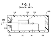
- Fig. 6 is a sectional view showing a conventional optical semiconductor module in the Japanese Patent Application Laid-Open No. 9-69585.
- a part of a semiconductor laser array 301 is fixed to a "V"-shaped groove formed in a Si substrate 303.
- An optical fiber array 343 is fixed to the Si substrate 303 with a fiber array-pressing plate 306 on the array 343.
- the Si substrate 303 is fixed to a bottom of a case 308 with AuSn solder paste.
- a cap 309 is located on the case 308.
- a fiber drawing-out mouth 310 is made in a housing composed of the case 308 and the cap 309. One end of the optical fiber array 343 is drawn out from the fiber drawing-out mouth 310 to the outside of the housing.
- Thermosetting resin 312 is beforehand applied to the fiber drawing-out mouth 310. By heating the case 308 and the cap 309, the thermosetting resin 312 is cured to seal the fiber drawing-out mouth 310. Grooves 311 for storing liquid resin are made in the fiber drawing-out mouth 310 in such a manner that the thermosetting resin 312 does not leak out by the thermal expansion of the inside of the housing.
- Japanese Patent Application Laid-Open No. 9-148592 discloses a process for sealing such a fiber drawing-out mouth as above, using resin having both photo-curing and thermosetting properties.
- the structure of the optical fiber drawing-out mouth 310 formed in the case 308 and the cap 309 is complicated. Therefore, the number of steps for producing the case 308 and the cap 309 is increased. Thus, there arises a problem that the optical semiconductor module becomes high-priced. Since the thermosetting resin 312 does not flow uniformly into the grooves 311 for storing liquid resin, air bubbles are incorporated into the thermosetting resin 312. Thus, when the resin 312 is cured, air-releasing paths are formed inside the resin 312. Therefore, moisture enters easily from the outside to the inside of the optical semiconductor module via these air-releasing paths. Thus, there also arises a problem that the optical semiconductor element (the laser array 301) inside the optical semiconductor module 300 is broken and the reliability thereof drops.
- the process disclosed in the Japanese Patent Application Laid-Open No. 9-148592 has a problem that the number of assembly steps increases by the double process composed of an photo-curing process based on irradiation with ultraviolet rays and a thermosetting process so that the optical semiconductor module becomes high-priced.
- An object of the present invention is to provide an optical semiconductor module making it possible to attain airtight sealing easily and surely and improve reliability at a low price; and a process for producing the same.
- an optical semiconductor module comprises: a housing having an opening; an optical semiconductor element provided in the housing; an optical fiber that penetrates the opening, the optical fiber performing optical transmission between the optical semiconductor element and an element arranged outside the housing; photo-curing resin sealing the opening; and a transparent plate arranged between the photo-curing resin and the outside of the housing.
- the opening that the optical fiber penetrates is sealed with the photo-curing resin in the present invention, air bubbles and the like are not produced and airtight sealing is certainly ensured. Thus, the reliability of the module is high. Since ultraviolet rays are radiated to the photo-curing resin through the transparent plate so that the photo-curing resin is cured, the number of producing steps can be decreased and costs can be reduced.
- the housing may comprise a case on which the optical semiconductor element is put, and a cap fitted onto this case, and the difference between the linear expansion coefficient of the photo-curing resin and that of the case may be less than 1 ⁇ 10 -5 /°C.
- the light transmission ratio of the transparent plate may be equal to or more than 98%. By setting the light transmission ratio of the transparent plate to 98% or more, it is possible to cure the photo-curing resin for fixing the optical fiber core line still more easily.
- the opening may comprise a concave opening portion having at least two stages, and the optical fiber and the transparent plate may be arranged on different stages from each other.
- the process for producing an optical semiconductor module comprises the steps of: putting an optical semiconductor element inside a case; and arranging an optical fiber in the case.
- the optical fiber performs optical transmission between the optical semiconductor element and an element arranged outside the case.
- the process further comprises the steps of: providing photo-curing resin to areas where side walls of the case and the optical fiber cross each other; putting a transparent plate on the photo-curing resin; and radiating light onto the photo-curing resin through the transparent plate to cure the photo-curing resin.
- the optical fiber is fixed to the case by curing the photo-curing resin.
- the number of producing steps is reduced, and air bubbles are not incorporated so that the reliability of the module is high.
- the difference between the linear expansion coefficient of the photo-curing resin and that of the case may be less than 1 ⁇ 10 -5 /°C, and the light transmission ratio of the transparent plate may be equal to or more than 98%.
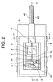
- FIG. 2 is a plan view showing an optical semiconductor module according to the first embodiment of the present invention.
- Fig. 3 is a sectional view taken along X-X line of Fig. 2.
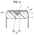
- Fig. 4 is a sectional view taken along Y-Y line of Fig. 2.
- a cap 9 is shown by an alternate long and two dashes line in order to make easy the grasp of the inner structure of the optical semiconductor module.
- a Si substrate 3 is fixed to the bottom of a case 8 with a conductive adhesive agent 205 such as a silver paste or a AuSn solder paste.
- a "V"-shaped V groove 32 is made in the Si substrate 3.
- a groove 31 is made in the direction perpendicular to the V groove 32 extending direction at the head of the V groove 32.
- An optical fiber core line 4 is fixed into the V groove 32 with ultraviolet ray-curing resin 203.
- a round optical fiber head sphere portion 41 is formed at one end of the optical fiber core line 4. This optical fiber head sphere portion 41 projects to the groove 31.
- a semiconductor laser element 1 as a light emitting element is positioned, oppositely to the optical fiber head sphere portion 41, on the Si substrate 3.
- the semiconductor laser element 1 is fixed to pattern electrodes made on the Si substrate 3 with AuSn solder paste.
- the optical axis of the semiconductor laser element 1 is consistent with that of the optical fiber core line 4.
- a monitoring photodiode-mounted chip carrier 5 is fixed to the bottom of the case 8 with conductive adhesive agent 206 such as silver paste or AuSn solder paste.
- a monitoring photodiode 2, which detects light emission of the semiconductor laser element 1, is mounted on the monitoring photodiode-mounted chip carrier 5.
- Metal terminals arranged in the Si substrate 3 and the monitoring photodiode-mounted chip carrier 5 are connected to desired metal terminals arranged inside the case 8 through bonding wires 44.
- a glass plate 6 for pressing the optical fiber core line 4 is selectively fixed onto the optical fiber core line 4 inside the groove 32 with ultraviolet ray-curing resin 203.
- the cap 9 is fixed onto the case 8 with ultraviolet ray-curing resin 201.
- the case 8 and the cap 9 may constitute a housing.
- a fiber drawing-out mouth 10 is made in the case 8. In the fiber drawing-out mouth 10, for example, two-stage concave portion is formed. The width of the upper-stage concave portion 10a is larger than that of the lower-stage concave portion 10b.
- the optical fiber core line 4 is fixed to the concave portion of the case 8 at the fiber drawing-out mouth 10 with an ultraviolet ray-curing resin 204.
- the glass plate 7 is fixed to the position between the cap 9 and the optical fiber core line 4 with the ultraviolet ray-curing resin 204.
- the cap 9 protects optical connection portions between the semiconductor laser element 1, the monitoring photodiode-mounted chip carrier 5 and the optical fiber from scattered light from the outside.
- the optical fiber core line 4 is coated with optical fiber coating material 42.
- a part of the optical fiber coating material 42 is fixed to the case 8 with ultraviolet ray-curing resin 202.
- optical semiconductor module of the first embodiment which has the above-mentioned structure.
- the semiconductor laser element 1 When a given voltage is applied to the semiconductor laser element 1 arranged on the Si substrate 3, the semiconductor laser element 1 emits laser light. This laser light strikes on the optical fiber head sphere portion 41, and passes through the optical fiber core line 4 to be output to elements and the like connected to the other end of the optical fiber core line 4. The laser light is also received by the monitoring photodiode 2, which is a light receiving element, and is converted to an electrical signal. This electrical signal is output from the terminal disposed at the case 8 through the monitoring photodiode-mounted chip carrier 5 and a bonding wire 44.
- Fig. 5 is a disassembly perspective view showing the process for producing the optical semiconductor module according to the first embodiment of the present invention.
- AuSn solder paste is, first, vapor-deposited on the pattern electrodes, which are arranged at the positions opposite to the V groove 32 sandwiching the groove 31 of the Si substrate 3 with the V groove 32.
- the semiconductor laser element 1 is fixed onto the electrodes with the AuSn solder paste. At this time, the fixation is performed in such precision that the gap between the center of the V groove and that of the semiconductor laser element 1 is within, e.g., ⁇ 1.5 ⁇ m.
- the Si substrate 3 and the monitoring photodiode-mounted chip carrier 5 are caused to adhere to the case 8 with the conductive adhesive agents 205 and 206 such as silver paste or AuSn solder paste. Subsequently, the metal terminals of the Si substrate 3 and the monitoring photodiode-mounted chip carrier 5 are bonded to desired metal terminals inside the case 8 with the bonding wires 44.
- the semiconductor laser element 1 is subjected to electric conduction screening (ACC). If an initial trouble is generated in the semiconductor laser element 1, the element 1 is removed.
- ACC electric conduction screening
- the optical fiber core line 4 is inserted from the fiber drawing-out mouth 10 to the V groove 32 made in the Si substrate 3.
- the ultraviolet ray-curing resin 203 is dropped onto the optical fiber core line 4 positioned in the V groove 32, and then the glass plate 6 for pressing the optical core line is set on the optical fiber core line 4. While a given pressure is applied to the glass plate 6 for pressing the optical core line from the upper thereof, ultraviolet rays are radiated to the resin 203, for example, under conditions that the intensity thereof is 95 mW/cm 2 and the radiation time thereof is 60 seconds. In this way, the optical fiber core line 4 is fixed into the V groove 32 of the Si substrate 3. At this time, by dropping the ultraviolet ray-curing resin 202 onto the periphery of the optical fiber coating material 42 and curing this material, the optical fiber coating material 42 is temporarily fixed to the case 8.
- the ultraviolet ray-curing resin 204 is dropped to the periphery of the optical fiber core line 4 positioned in the lower-step concave portion 10b of the fiber drawing-out mouth 10, and then the glass plate 8 having a light-transmission ratio of, for example, 98% or more is put on the upper-step concave 10a of the fiber drawing-out mouth 10.
- the glass plate 8 is pressed against the concave portion 10a and subsequently ultraviolet rays are uniformly radiated from three directions, for example, to the ultraviolet ray-curing resin 204, for example, under conditions that the intensity thereof is 200 mW/cm 2 and the radiation time thereof is 60 seconds.
- the ultraviolet rays sufficiently reach every part of the lower-concave portion 10b and the ultraviolet ray-curing resin 204 is cured so that the optical fiber core line 4 is fixed to the case 8.
- the ultraviolet ray-curing resin 201 is applied to given areas of the case 8 and the glass plate 7, and then the cap 9 is put on the case 8 in place.
- the ultraviolet ray-curing resin 201 is cured by radiation of ultraviolet rays.
- the cap 9 is fixed onto the case 8, so that the fiber drawing-out mouth 10 is sealed.
- the ultraviolet ray-curing resin 202 is applied to the periphery of the optical fiber 43. By curing this resin, the optical fiber 43 is fixed to the case 8.
- the fiber drawing-out mouth 10 can be sealed only by dropping of the ultraviolet ray-curing resin 204 and the curing of the ultraviolet ray-curing resin 204 through the radiation of the ultraviolet rays. Since the glass plate 7 makes it possible to prevent flowing-out of the ultraviolet ray-curing resin 204 and the positioning of the optical fiber core line 4, it is possible to prevent incorporation of the moisture from the outside and a deterioration in output.
- the semiconductor laser element which is a light emitting element
- the optical semiconductor element may be a different element such as any different light emitting element, a light receiving element, or a semiconductor optical amplifier.
- the ultraviolet ray-curing resin 202 is used but thermosetting resin or the like may be used.
- the first embodiment has a structure wherein a laser signal output from the semiconductor laser element is optically transmitted through a single optical fiber, but may be a structure wherein plural laser signals are optically transmitted through an optical fiber array having plural optical fibers, using a device having plural light emitting elements, for example, a semiconductor laser array.
- Fig. 6 is a plan view showing the optical semiconductor module according to the second embodiment of the present invention.
- a cap 9 is shown by an alternate long and two dashes line in order to make easy the grasp of the inner structure of the optical semiconductor module.
- the same reference numbers as in Fig. 6 are attached to the same constituents as in the first embodiment shown in Fig. 2, and the explanation thereof is omitted.
- plural "V"-shaped grooves are made in the Si substrate 3.
- Plural optical fiber core lines are fixed into these grooves with, for example, an ultraviolet ray-curing resin.
- the plural optical fiber core lines may constitute a tape-form optical fiber array 443.
- the periphery of the tape-form optical fiber array 443 is coated with a coating material (non shown). These constitute an optical fiber 42a.
- a semiconductor laser array 401 comprising plural semiconductor laser elements is arranged oppositely to the top end of the tape-form optical fiber array 443 inside the housing. The optical axis of the semiconductor laser array 401 is consistent with that of the tape-form optical fiber array 443.
- An optical fiber array-pressing plate 406 is selectively fixed onto the tape-form optical fiber array 443 inside the V grooves with ultraviolet ray-curing resin.
- the glass plate 7 is fixed to the fiber drawing-out mouth 10 with an ultraviolet ray-curing resin.
- the optical semiconductor module having such a structure can be produced by substantially the same steps as for producing the optical semiconductor module of the first embodiment. That is, the ultraviolet ray-curing resin is dropped onto the tape-form optical fiber array 443 inside the V grooves. While the optical fiber array-pressing plate 406 is pressed against the tape-form optical fiber array 443, ultraviolet rays are radiated to the resin. In this way, this ultraviolet ray-curing resin is cured. Thereafter, in the fiber drawing-out mouth 10, the ultraviolet ray-curing resin is dropped onto the periphery of the tape-form optical fiber array 443, and then the glass plate 7 is put on the upper-concave portion of the fiber drawing-out mouth 10. Ultraviolet rays are then radiated thereto, so as to cure the ultraviolet ray-curing resin.
- the following it is desired to set the following to less than 1 ⁇ 10 -5 /°C in order to prevent cracks upon the curing of the resin: the difference between the linear expansion coefficient of the ultraviolet ray-curing resin used in the sealing of the fiber drawing-out mouth 10 and that of the case.
- air bubbles are not produced and airtight sealing can be easily and surely attained because an opening that an optical fiber penetrates is sealed with a photo-curing resin. Therefore, the reliability of an optical semiconductor module can be improved. Moreover, the number of producing steps can be decreased so that costs can be reduced. Furthermore, optical fibers can be still more easily fixed by making a concave opening portion having at least two steps in the opening.
Landscapes
- Physics & Mathematics (AREA)
- General Physics & Mathematics (AREA)
- Optics & Photonics (AREA)
- Optical Couplings Of Light Guides (AREA)
- Led Devices (AREA)
- Semiconductor Lasers (AREA)
- Light Receiving Elements (AREA)
Abstract
Description
- The present invention relates to an optical semiconductor module comprising an optical element composed of a light emitting element (a laser diode: LD) or a light receiving element (a photodiode: PD), and an optical fiber optically connected to the optical element; and a process for producing the same. The present invention relates specifically to an optical semiconductor module making it possible to attain airtight sealing easily and surely, and a process for producing the same.
- As optical fiber communication has been spreading recently, for an optical semiconductor module used in the optical fiber communication, a low-priced module whose assembly process is made simple has been demanded. For this purpose, there is generally used a module wherein a semiconductor laser element as a light emitting element and an optical fiber are mounted on a single Si substrate. In this case, the strand of the optical fiber is bonded to a "V"-shaped groove made in the Si substrate at a given position with a resin or a solder material (such as AuSn) as an adhesive agent, and is fixed with an optical fiber-pressing plate. The optical fiber is drawn out from an optical fiber drawing-out mouth made in a housing to the outside of the housing. As a sealing material for the optical fiber drawing-out mouth, there is used a solder paste comprising AuSn, PbSn or the like, a low melting-point glass or a resin.
- However, in the case that the solder paste is used, in order to enhance close adhesion between the optical fiber and the solder paste, it is necessary that a surface of the optical fiber is subjected to metal processing such as Au plating. Thus, the number of processing steps increase. For this reason, the optical semiconductor module becomes high-priced. In the case that the low melting-point glass is used, it is necessary to heat the optical fiber drawing-out mouth up to 430-470°C, at which the low melting-point glass is melted. Therefore, the solder paste with which the optical fiber is fixed to the substrate in the housing is melted so that the positional relationship between the semiconductor laser and the optical fiber gets off. As a result, there arises a problem that a desired optical fiber output cannot be obtained.
- Thus, Japanese Patent Application Laid-Open No. 9-69585 discloses a process using resin as a process for sealing an optical fiber drawing-out mouth. Fig. 6 is a sectional view showing a conventional optical semiconductor module in the Japanese Patent Application Laid-Open No. 9-69585. In this conventional optical semiconductor module, a part of a
semiconductor laser array 301 is fixed to a "V"-shaped groove formed in aSi substrate 303. Anoptical fiber array 343 is fixed to theSi substrate 303 with a fiber array-pressing plate 306 on thearray 343. The Sisubstrate 303 is fixed to a bottom of acase 308 with AuSn solder paste. Acap 309 is located on thecase 308. A fiber drawing-outmouth 310 is made in a housing composed of thecase 308 and thecap 309. One end of theoptical fiber array 343 is drawn out from the fiber drawing-outmouth 310 to the outside of the housing. -
Thermosetting resin 312 is beforehand applied to the fiber drawing-outmouth 310. By heating thecase 308 and thecap 309, thethermosetting resin 312 is cured to seal the fiber drawing-outmouth 310.Grooves 311 for storing liquid resin are made in the fiber drawing-outmouth 310 in such a manner that thethermosetting resin 312 does not leak out by the thermal expansion of the inside of the housing. - Japanese Patent Application Laid-Open No. 9-148592 discloses a process for sealing such a fiber drawing-out mouth as above, using resin having both photo-curing and thermosetting properties.
- However, in the conventional optical semiconductor module disclosed in the Japanese Patent Application Laid-Open No. 9-69585, the structure of the optical fiber drawing-out
mouth 310 formed in thecase 308 and thecap 309 is complicated. Therefore, the number of steps for producing thecase 308 and thecap 309 is increased. Thus, there arises a problem that the optical semiconductor module becomes high-priced. Since thethermosetting resin 312 does not flow uniformly into thegrooves 311 for storing liquid resin, air bubbles are incorporated into thethermosetting resin 312. Thus, when theresin 312 is cured, air-releasing paths are formed inside theresin 312. Therefore, moisture enters easily from the outside to the inside of the optical semiconductor module via these air-releasing paths. Thus, there also arises a problem that the optical semiconductor element (the laser array 301) inside theoptical semiconductor module 300 is broken and the reliability thereof drops. - The process disclosed in the Japanese Patent Application Laid-Open No. 9-148592 has a problem that the number of assembly steps increases by the double process composed of an photo-curing process based on irradiation with ultraviolet rays and a thermosetting process so that the optical semiconductor module becomes high-priced.
- An object of the present invention is to provide an optical semiconductor module making it possible to attain airtight sealing easily and surely and improve reliability at a low price; and a process for producing the same.
- According to one aspect of the present invention, an optical semiconductor module comprises: a housing having an opening; an optical semiconductor element provided in the housing; an optical fiber that penetrates the opening, the optical fiber performing optical transmission between the optical semiconductor element and an element arranged outside the housing; photo-curing resin sealing the opening; and a transparent plate arranged between the photo-curing resin and the outside of the housing.
- Since the opening that the optical fiber penetrates is sealed with the photo-curing resin in the present invention, air bubbles and the like are not produced and airtight sealing is certainly ensured. Thus, the reliability of the module is high. Since ultraviolet rays are radiated to the photo-curing resin through the transparent plate so that the photo-curing resin is cured, the number of producing steps can be decreased and costs can be reduced.
- In the present invention, the housing may comprise a case on which the optical semiconductor element is put, and a cap fitted onto this case, and the difference between the linear expansion coefficient of the photo-curing resin and that of the case may be less than 1 × 10⁻⁵ /°C. By setting the difference between the linear expansion coefficients to less than 1 × 10⁻⁵ /°C, it is possible to prevent generation of cracks based on a change in external temperature or the like, and improve certainty of airtight sealing.
- The light transmission ratio of the transparent plate may be equal to or more than 98%. By setting the light transmission ratio of the transparent plate to 98% or more, it is possible to cure the photo-curing resin for fixing the optical fiber core line still more easily.
- The opening may comprise a concave opening portion having at least two stages, and the optical fiber and the transparent plate may be arranged on different stages from each other.
- According to another aspect of the present invention, the process for producing an optical semiconductor module comprises the steps of: putting an optical semiconductor element inside a case; and arranging an optical fiber in the case. The optical fiber performs optical transmission between the optical semiconductor element and an element arranged outside the case. The process further comprises the steps of: providing photo-curing resin to areas where side walls of the case and the optical fiber cross each other; putting a transparent plate on the photo-curing resin; and radiating light onto the photo-curing resin through the transparent plate to cure the photo-curing resin.
- In the process according to the present invention, the optical fiber is fixed to the case by curing the photo-curing resin. Thus, the number of producing steps is reduced, and air bubbles are not incorporated so that the reliability of the module is high.
- In the process, the difference between the linear expansion coefficient of the photo-curing resin and that of the case may be less than 1 × 10⁻⁵ /°C, and the light transmission ratio of the transparent plate may be equal to or more than 98%.
- Fig. 1 is a sectional view showing a conventional optical semiconductor module.
- Fig. 2 is a plan view showing an optical semiconductor module according to a first embodiment of the present invention.
- Fig. 3 is a sectional view taken along X-X line of Fig. 2, showing the optical semiconductor module according to the first embodiment of the present invention.
- Fig. 4 is a sectional view taken along Y-Y line of Fig. 2, showing the optical semiconductor module according to the first embodiment of the present invention.
- Fig. 5 is a disassembly perspective view showing a process for producing the optical semiconductor module according to the first embodiment of the present invention.
- Fig. 6 is a plan view showing an optical semiconductor module according to a second embodiment of the present invention.
-
- Referring to the attached drawings, an optical semiconductor module according to a first embodiment of the present invention will be specifically described. Fig. 2 is a plan view showing an optical semiconductor module according to the first embodiment of the present invention. Fig. 3 is a sectional view taken along X-X line of Fig. 2. Fig. 4 is a sectional view taken along Y-Y line of Fig. 2. In Fig. 2, a
cap 9 is shown by an alternate long and two dashes line in order to make easy the grasp of the inner structure of the optical semiconductor module. - As shown in Figs. 2 to 4, in the first embodiment, a
Si substrate 3 is fixed to the bottom of acase 8 with a conductiveadhesive agent 205 such as a silver paste or a AuSn solder paste. A "V"-shaped V groove 32 is made in theSi substrate 3. Agroove 31 is made in the direction perpendicular to theV groove 32 extending direction at the head of theV groove 32. An opticalfiber core line 4 is fixed into theV groove 32 with ultraviolet ray-curing resin 203. A round optical fiberhead sphere portion 41 is formed at one end of the opticalfiber core line 4. This optical fiberhead sphere portion 41 projects to thegroove 31. Asemiconductor laser element 1 as a light emitting element is positioned, oppositely to the optical fiberhead sphere portion 41, on theSi substrate 3. Thesemiconductor laser element 1 is fixed to pattern electrodes made on theSi substrate 3 with AuSn solder paste. The optical axis of thesemiconductor laser element 1 is consistent with that of the opticalfiber core line 4. - A monitoring photodiode-mounted
chip carrier 5 is fixed to the bottom of thecase 8 with conductiveadhesive agent 206 such as silver paste or AuSn solder paste. Amonitoring photodiode 2, which detects light emission of thesemiconductor laser element 1, is mounted on the monitoring photodiode-mountedchip carrier 5. Metal terminals arranged in theSi substrate 3 and the monitoring photodiode-mountedchip carrier 5 are connected to desired metal terminals arranged inside thecase 8 throughbonding wires 44. - A
glass plate 6 for pressing the opticalfiber core line 4 is selectively fixed onto the opticalfiber core line 4 inside thegroove 32 with ultraviolet ray-curingresin 203. Thecap 9 is fixed onto thecase 8 with ultraviolet ray-curingresin 201. Thecase 8 and thecap 9 may constitute a housing. A fiber drawing-outmouth 10 is made in thecase 8. In the fiber drawing-outmouth 10, for example, two-stage concave portion is formed. The width of the upper-stageconcave portion 10a is larger than that of the lower-stageconcave portion 10b. - The optical
fiber core line 4 is fixed to the concave portion of thecase 8 at the fiber drawing-outmouth 10 with an ultraviolet ray-curingresin 204. Moreover, theglass plate 7 is fixed to the position between thecap 9 and the opticalfiber core line 4 with the ultraviolet ray-curingresin 204. Thecap 9 protects optical connection portions between thesemiconductor laser element 1, the monitoring photodiode-mountedchip carrier 5 and the optical fiber from scattered light from the outside. - In the outside of the
cap 9, the opticalfiber core line 4 is coated with opticalfiber coating material 42. A part of the opticalfiber coating material 42 is fixed to thecase 8 with ultraviolet ray-curingresin 202. - The following will describe operation of the optical semiconductor module of the first embodiment, which has the above-mentioned structure.
- When a given voltage is applied to the
semiconductor laser element 1 arranged on theSi substrate 3, thesemiconductor laser element 1 emits laser light. This laser light strikes on the optical fiberhead sphere portion 41, and passes through the opticalfiber core line 4 to be output to elements and the like connected to the other end of the opticalfiber core line 4. The laser light is also received by themonitoring photodiode 2, which is a light receiving element, and is converted to an electrical signal. This electrical signal is output from the terminal disposed at thecase 8 through the monitoring photodiode-mountedchip carrier 5 and abonding wire 44. - The following will describe a process for producing the optical semiconductor module according to the first embodiment. Fig. 5 is a disassembly perspective view showing the process for producing the optical semiconductor module according to the first embodiment of the present invention.
- As shown in Fig. 5, AuSn solder paste is, first, vapor-deposited on the pattern electrodes, which are arranged at the positions opposite to the
V groove 32 sandwiching thegroove 31 of theSi substrate 3 with theV groove 32. Thesemiconductor laser element 1 is fixed onto the electrodes with the AuSn solder paste. At this time, the fixation is performed in such precision that the gap between the center of the V groove and that of thesemiconductor laser element 1 is within, e.g., ±1.5 µm. - Next, the
Si substrate 3 and the monitoring photodiode-mountedchip carrier 5 are caused to adhere to thecase 8 with the conductiveadhesive agents Si substrate 3 and the monitoring photodiode-mountedchip carrier 5 are bonded to desired metal terminals inside thecase 8 with thebonding wires 44. Next, thesemiconductor laser element 1 is subjected to electric conduction screening (ACC). If an initial trouble is generated in thesemiconductor laser element 1, theelement 1 is removed. - Next, the optical
fiber core line 4 is inserted from the fiber drawing-outmouth 10 to theV groove 32 made in theSi substrate 3. Thereafter, the ultraviolet ray-curingresin 203 is dropped onto the opticalfiber core line 4 positioned in theV groove 32, and then theglass plate 6 for pressing the optical core line is set on the opticalfiber core line 4. While a given pressure is applied to theglass plate 6 for pressing the optical core line from the upper thereof, ultraviolet rays are radiated to theresin 203, for example, under conditions that the intensity thereof is 95 mW/cm2 and the radiation time thereof is 60 seconds. In this way, the opticalfiber core line 4 is fixed into theV groove 32 of theSi substrate 3. At this time, by dropping the ultraviolet ray-curingresin 202 onto the periphery of the opticalfiber coating material 42 and curing this material, the opticalfiber coating material 42 is temporarily fixed to thecase 8. - Next, the ultraviolet ray-curing
resin 204 is dropped to the periphery of the opticalfiber core line 4 positioned in the lower-stepconcave portion 10b of the fiber drawing-outmouth 10, and then theglass plate 8 having a light-transmission ratio of, for example, 98% or more is put on the upper-step concave 10a of the fiber drawing-outmouth 10. Theglass plate 8 is pressed against theconcave portion 10a and subsequently ultraviolet rays are uniformly radiated from three directions, for example, to the ultraviolet ray-curingresin 204, for example, under conditions that the intensity thereof is 200 mW/cm2 and the radiation time thereof is 60 seconds. In this way, the ultraviolet rays sufficiently reach every part of the lower-concave portion 10b and the ultraviolet ray-curingresin 204 is cured so that the opticalfiber core line 4 is fixed to thecase 8. Next, the ultraviolet ray-curingresin 201 is applied to given areas of thecase 8 and theglass plate 7, and then thecap 9 is put on thecase 8 in place. Next, the ultraviolet ray-curingresin 201 is cured by radiation of ultraviolet rays. Thus, thecap 9 is fixed onto thecase 8, so that the fiber drawing-outmouth 10 is sealed. - Next, for example, the ultraviolet ray-curing
resin 202 is applied to the periphery of theoptical fiber 43. By curing this resin, theoptical fiber 43 is fixed to thecase 8. - In such a producing process, the fiber drawing-out
mouth 10 can be sealed only by dropping of the ultraviolet ray-curingresin 204 and the curing of the ultraviolet ray-curingresin 204 through the radiation of the ultraviolet rays. Since theglass plate 7 makes it possible to prevent flowing-out of the ultraviolet ray-curingresin 204 and the positioning of the opticalfiber core line 4, it is possible to prevent incorporation of the moisture from the outside and a deterioration in output. - In the first embodiment, the semiconductor laser element, which is a light emitting element, is used as the optical semiconductor element. However, the optical semiconductor element may be a different element such as any different light emitting element, a light receiving element, or a semiconductor optical amplifier. In order to fix the
optical fiber 43, the ultraviolet ray-curingresin 202 is used but thermosetting resin or the like may be used. - The first embodiment has a structure wherein a laser signal output from the semiconductor laser element is optically transmitted through a single optical fiber, but may be a structure wherein plural laser signals are optically transmitted through an optical fiber array having plural optical fibers, using a device having plural light emitting elements, for example, a semiconductor laser array.
- The following will describe an optical semiconductor module using a semiconductor laser array according to a second embodiment of the present invention. Fig. 6 is a plan view showing the optical semiconductor module according to the second embodiment of the present invention. In Fig. 6, a
cap 9 is shown by an alternate long and two dashes line in order to make easy the grasp of the inner structure of the optical semiconductor module. The same reference numbers as in Fig. 6 are attached to the same constituents as in the first embodiment shown in Fig. 2, and the explanation thereof is omitted. - In the second embodiment, plural "V"-shaped grooves are made in the
Si substrate 3. Plural optical fiber core lines are fixed into these grooves with, for example, an ultraviolet ray-curing resin. The plural optical fiber core lines may constitute a tape-formoptical fiber array 443. In the outside of thecase 8, the periphery of the tape-formoptical fiber array 443 is coated with a coating material (non shown). These constitute anoptical fiber 42a. Asemiconductor laser array 401 comprising plural semiconductor laser elements is arranged oppositely to the top end of the tape-formoptical fiber array 443 inside the housing. The optical axis of thesemiconductor laser array 401 is consistent with that of the tape-formoptical fiber array 443. - An optical fiber array-pressing
plate 406 is selectively fixed onto the tape-formoptical fiber array 443 inside the V grooves with ultraviolet ray-curing resin. Theglass plate 7 is fixed to the fiber drawing-outmouth 10 with an ultraviolet ray-curing resin. - The optical semiconductor module having such a structure can be produced by substantially the same steps as for producing the optical semiconductor module of the first embodiment. That is, the ultraviolet ray-curing resin is dropped onto the tape-form
optical fiber array 443 inside the V grooves. While the optical fiber array-pressingplate 406 is pressed against the tape-formoptical fiber array 443, ultraviolet rays are radiated to the resin. In this way, this ultraviolet ray-curing resin is cured. Thereafter, in the fiber drawing-outmouth 10, the ultraviolet ray-curing resin is dropped onto the periphery of the tape-formoptical fiber array 443, and then theglass plate 7 is put on the upper-concave portion of the fiber drawing-outmouth 10. Ultraviolet rays are then radiated thereto, so as to cure the ultraviolet ray-curing resin. - In the first and second embodiments, it is desired to set the following to less than 1 × 10⁻⁵ /°C in order to prevent cracks upon the curing of the resin: the difference between the linear expansion coefficient of the ultraviolet ray-curing resin used in the sealing of the fiber drawing-out
mouth 10 and that of the case. - According to the present invention, air bubbles are not produced and airtight sealing can be easily and surely attained because an opening that an optical fiber penetrates is sealed with a photo-curing resin. Therefore, the reliability of an optical semiconductor module can be improved. Moreover, the number of producing steps can be decreased so that costs can be reduced. Furthermore, optical fibers can be still more easily fixed by making a concave opening portion having at least two steps in the opening.
Claims (7)
- An optical semiconductor module comprising:a housing (8, 9) having an opening (10);an optical semiconductor element (1) provided in said housing (8, 9);an optical fiber (43) that penetrates said opening (10), said optical fiber (43) performing optical transmission between said optical semiconductor element (1) and an element arranged outside said housing;photo-curing resin (204) sealing said opening (10); anda transparent plate (7) arranged between said photo-curing resin (204) and the outside of said housing (8, 9).
- The optical semiconductor module according to claim 1,
characterized in thatsaid housing (8, 9) comprises a case (8) on which said optical semiconductor element (1) is mounted, and a cap (9) fitted to said case (8), and the difference between the linear expansion coefficient of said photo-curing resin (204) and that of said case (8) is less than 1 x 10⁻⁵/°C. - The optical semiconductor module according to claim 1 or 2, characterized in that the light transmission ratio of said transparent plate (7) is equal to or more than 98%.
- The optical semiconductor module according to claim 1, 2 or 3, characterized in thatsaid opening (10) comprises a concave opening portion having at least two stages (10a, 10b), andsaid optical fiber (43) and said transparent plate (7) are arranged on different stages (10a, 10b) from each other.
- A process for producing an optical semiconductor module comprising the steps of:putting an optical semiconductor element (1) inside a case (8);arranging an optical fiber (43) in said case (8), said optical fiber (43) performing optical transmission between said optical semiconductor element (1) and an element arranged outside said case (8);providing photo-curing resin (204) to areas where side walls of said case (8) and said optical fiber (43) cross each other;putting a transparent plate (7) on said photocuring resin (204); andradiating light onto said photo-curing resin (204) through said transparent plate (7) to cure said photo-curing resin (204).
- The process according to claim 5, characterized in that the difference between the linear expansion coefficient of said photo-curing resin (204) and that of said case (8) is less than 1 x 10⁻⁵/°C.
- The process according to claim 5 or 6, characterized in that the light transmission ratio of said transparent plate (7) is equal to or more than 98%.
Applications Claiming Priority (2)
| Application Number | Priority Date | Filing Date | Title |
|---|---|---|---|
| JP09574599A JP3459787B2 (en) | 1999-04-02 | 1999-04-02 | Optical semiconductor module and manufacturing method thereof |
| JP9574599 | 1999-04-02 |
Publications (1)
| Publication Number | Publication Date |
|---|---|
| EP1041419A1 true EP1041419A1 (en) | 2000-10-04 |
Family
ID=14146041
Family Applications (1)
| Application Number | Title | Priority Date | Filing Date |
|---|---|---|---|
| EP00106943A Withdrawn EP1041419A1 (en) | 1999-04-02 | 2000-03-31 | Optical semiconductor module with fiber connection and its assembly process |
Country Status (3)
| Country | Link |
|---|---|
| US (1) | US6485197B1 (en) |
| EP (1) | EP1041419A1 (en) |
| JP (1) | JP3459787B2 (en) |
Cited By (2)
| Publication number | Priority date | Publication date | Assignee | Title |
|---|---|---|---|---|
| WO2004049526A1 (en) * | 2002-11-12 | 2004-06-10 | Matsushita Electric Industrial Co., Ltd. | Laser module and its fabrication method |
| CN102834754A (en) * | 2010-02-23 | 2012-12-19 | 松下电器产业株式会社 | Optical module |
Families Citing this family (15)
| Publication number | Priority date | Publication date | Assignee | Title |
|---|---|---|---|---|
| TW527676B (en) * | 2001-01-19 | 2003-04-11 | Matsushita Electric Industrial Co Ltd | Photo-semiconductor module and method for manufacturing |
| US6837627B2 (en) * | 2001-04-25 | 2005-01-04 | Sumitomo Electric Industries, Ltd. | Optical communication module |
| JP4583662B2 (en) * | 2001-06-01 | 2010-11-17 | 三菱電機株式会社 | Optical module package and manufacturing method thereof |
| JP2003066290A (en) * | 2001-08-29 | 2003-03-05 | Sumitomo Electric Ind Ltd | Optical communication module |
| JP2003069054A (en) * | 2001-08-29 | 2003-03-07 | Sumitomo Electric Ind Ltd | Optical communication module |
| JP3838140B2 (en) * | 2002-04-05 | 2006-10-25 | 日立電線株式会社 | Multi-channel optical transceiver |
| JP4134695B2 (en) * | 2002-11-21 | 2008-08-20 | 住友電気工業株式会社 | Optical module |
| US6856717B2 (en) * | 2003-03-24 | 2005-02-15 | Hymite A/S | Package with a light emitting device |
| US8545111B2 (en) * | 2007-06-28 | 2013-10-01 | Nippon Telegraph And Telephone Corporation | Optical module |
| FR2962231B1 (en) * | 2010-07-02 | 2014-10-31 | Alcatel Lucent | METHOD FOR ALIGNING AND FIXING AN OPTICAL FIBER COUPLED WITH AN OPTOELECTRONIC COMPONENT |
| JP2014077914A (en) * | 2012-10-11 | 2014-05-01 | Rohm Co Ltd | Optical communication module and manufacturing method therefor |
| JP2014077915A (en) * | 2012-10-11 | 2014-05-01 | Rohm Co Ltd | Optical communication module and manufacturing method therefor |
| JP6417677B2 (en) * | 2014-03-07 | 2018-11-07 | 富士通オプティカルコンポーネンツ株式会社 | Optical module and optical modulator |
| WO2019207744A1 (en) * | 2018-04-26 | 2019-10-31 | オリンパス株式会社 | Optical module for endoscope, endoscope, and method for manufacturing optical module for endoscope |
| CN111352192B (en) * | 2018-12-20 | 2021-08-10 | 青岛海信宽带多媒体技术有限公司 | Optical module |
Citations (6)
| Publication number | Priority date | Publication date | Assignee | Title |
|---|---|---|---|---|
| JPS61290413A (en) * | 1985-06-19 | 1986-12-20 | Hitachi Ltd | Optical fiber transmission module |
| EP0399684A2 (en) * | 1989-05-22 | 1990-11-28 | Tektronix Inc. | Laser pigtail assembly and method of manufacture |
| US5048912A (en) * | 1988-03-09 | 1991-09-17 | Fujitsu Limited | Optical fiber switching with spherical lens and method of making same |
| EP0644442A1 (en) * | 1993-04-02 | 1995-03-22 | The Furukawa Electric Co., Ltd. | Terminal of optical fiber, method of its manufacture, and structure for connecting the terminal and optical device |
| EP0704731A2 (en) * | 1994-09-28 | 1996-04-03 | Kabushiki Kaisha Toshiba | Optical semiconductor module & method for manufacturing the same |
| EP0872748A2 (en) * | 1997-04-18 | 1998-10-21 | Nec Corporation | Method for hermetically sealing optical fiber feedthrough and hermetically sealed structure |
Family Cites Families (7)
| Publication number | Priority date | Publication date | Assignee | Title |
|---|---|---|---|---|
| DE69426347T2 (en) * | 1993-09-29 | 2001-05-17 | Matsushita Electric Industrial Co., Ltd. | Method of mounting a semiconductor device on a circuit board and a circuit board with a semiconductor device thereon |
| JPH08335744A (en) | 1995-06-06 | 1996-12-17 | Hitachi Ltd | Optical semiconductor module and assembling method thereof |
| JPH0969585A (en) | 1995-08-31 | 1997-03-11 | Mitsubishi Electric Corp | Electronic component mounting apparatus and hermetically sealing method thereof |
| US6067392A (en) * | 1995-10-16 | 2000-05-23 | Sumitomo Electric Industries, Ltd. | Optical fiber diffraction grating, a method of fabricating thereof and a laser light source |
| JPH09148592A (en) | 1995-11-21 | 1997-06-06 | Hitachi Ltd | Optical communication module and manufacturing method thereof |
| JPH1131751A (en) * | 1997-07-10 | 1999-02-02 | Sony Corp | Hollow package and manufacturing method thereof |
| US6130444A (en) * | 1998-02-27 | 2000-10-10 | Nec Corporation | Optical fiber secured with a photosetting resin covered with a UV light-transmissive plate |
-
1999
- 1999-04-02 JP JP09574599A patent/JP3459787B2/en not_active Expired - Fee Related
-
2000
- 2000-03-30 US US09/538,906 patent/US6485197B1/en not_active Expired - Fee Related
- 2000-03-31 EP EP00106943A patent/EP1041419A1/en not_active Withdrawn
Patent Citations (6)
| Publication number | Priority date | Publication date | Assignee | Title |
|---|---|---|---|---|
| JPS61290413A (en) * | 1985-06-19 | 1986-12-20 | Hitachi Ltd | Optical fiber transmission module |
| US5048912A (en) * | 1988-03-09 | 1991-09-17 | Fujitsu Limited | Optical fiber switching with spherical lens and method of making same |
| EP0399684A2 (en) * | 1989-05-22 | 1990-11-28 | Tektronix Inc. | Laser pigtail assembly and method of manufacture |
| EP0644442A1 (en) * | 1993-04-02 | 1995-03-22 | The Furukawa Electric Co., Ltd. | Terminal of optical fiber, method of its manufacture, and structure for connecting the terminal and optical device |
| EP0704731A2 (en) * | 1994-09-28 | 1996-04-03 | Kabushiki Kaisha Toshiba | Optical semiconductor module & method for manufacturing the same |
| EP0872748A2 (en) * | 1997-04-18 | 1998-10-21 | Nec Corporation | Method for hermetically sealing optical fiber feedthrough and hermetically sealed structure |
Non-Patent Citations (1)
| Title |
|---|
| PATENT ABSTRACTS OF JAPAN vol. 011, no. 156 (P - 578) 21 May 1987 (1987-05-21) * |
Cited By (5)
| Publication number | Priority date | Publication date | Assignee | Title |
|---|---|---|---|---|
| WO2004049526A1 (en) * | 2002-11-12 | 2004-06-10 | Matsushita Electric Industrial Co., Ltd. | Laser module and its fabrication method |
| CN100358196C (en) * | 2002-11-12 | 2007-12-26 | 松下电器产业株式会社 | Laser module and manufacturing method thereof |
| US7494286B2 (en) | 2002-11-12 | 2009-02-24 | Panasonic Corporation | Laser module and method for manufacturing the same |
| CN102834754A (en) * | 2010-02-23 | 2012-12-19 | 松下电器产业株式会社 | Optical module |
| CN102834754B (en) * | 2010-02-23 | 2015-11-25 | 松下知识产权经营株式会社 | Optical module |
Also Published As
| Publication number | Publication date |
|---|---|
| JP3459787B2 (en) | 2003-10-27 |
| JP2000294835A (en) | 2000-10-20 |
| US6485197B1 (en) | 2002-11-26 |
Similar Documents
| Publication | Publication Date | Title |
|---|---|---|
| US6485197B1 (en) | Optical semiconductor module and process for producing the same | |
| US6282350B1 (en) | Photoelectronic device and method of manufacturing the same | |
| US6739764B2 (en) | Optical module and optical communication system | |
| US6461059B2 (en) | Photo-electronic device and method of producing the same | |
| US6467972B2 (en) | Optical interconnection module | |
| US6425695B1 (en) | Optical module and method of manufacturing the same | |
| US5309460A (en) | Semiconductor laser with encapsulated lead members | |
| US6130444A (en) | Optical fiber secured with a photosetting resin covered with a UV light-transmissive plate | |
| US6550982B2 (en) | Optoelectronic surface-mountable module and optoelectronic coupling unit | |
| CN1779970B (en) | Optical rotation system for optoelectronic modules | |
| US6368890B1 (en) | Top contact VCSEL with monitor | |
| US6188118B1 (en) | Semiconductor photodetector packaging | |
| US20050056851A1 (en) | Optoelectronic component and optoelectronic arrangement with an optoelectronic component | |
| JP2002534813A (en) | Photon device sealing method and device | |
| US6476379B2 (en) | Optoelectronic devices and manufacturing method thereof | |
| US6407438B1 (en) | Semiconductor opto-electronic device packaging | |
| US5945688A (en) | Optical semiconductor device and lead frame used in such a device | |
| JP3543189B2 (en) | Semiconductor element package and semiconductor device | |
| US20030031426A1 (en) | Fiber with ferrule, and optical module and method of manufacturing the same | |
| JP2000156510A (en) | Opto-semiconductor element, method of manufacturing opto-semiconductor element, and optoelectronic device | |
| JP3717623B2 (en) | Optoelectronic device and manufacturing method thereof | |
| JP3334829B2 (en) | Optical semiconductor module | |
| JP3415468B2 (en) | Optical semiconductor device | |
| JP3240980B2 (en) | Method of manufacturing semiconductor module device | |
| JP3481016B2 (en) | Terminal for optical fiber array and terminal for optical fiber array equipped with optical semiconductor chip array |
Legal Events
| Date | Code | Title | Description |
|---|---|---|---|
| PUAI | Public reference made under article 153(3) epc to a published international application that has entered the european phase |
Free format text: ORIGINAL CODE: 0009012 |
|
| 17P | Request for examination filed |
Effective date: 20000720 |
|
| AK | Designated contracting states |
Kind code of ref document: A1 Designated state(s): DE DK FR GB IT |
|
| AX | Request for extension of the european patent |
Free format text: AL;LT;LV;MK;RO;SI |
|
| AKX | Designation fees paid |
Free format text: DE DK FR GB IT |
|
| DBV | Designated contracting states (deleted) | ||
| RBV | Designated contracting states (corrected) |
Designated state(s): DE DK FR GB IT |
|
| RAP1 | Party data changed (applicant data changed or rights of an application transferred) |
Owner name: NEC COMPOUND SEMICONDUCTOR DEVICES, LTD. |
|
| 17Q | First examination report despatched |
Effective date: 20050125 |
|
| STAA | Information on the status of an ep patent application or granted ep patent |
Free format text: STATUS: THE APPLICATION HAS BEEN WITHDRAWN |
|
| 18W | Application withdrawn |
Effective date: 20050414 |