EP1039665A2 - Optical transmitter circuit - Google Patents
Optical transmitter circuit Download PDFInfo
- Publication number
- EP1039665A2 EP1039665A2 EP00101267A EP00101267A EP1039665A2 EP 1039665 A2 EP1039665 A2 EP 1039665A2 EP 00101267 A EP00101267 A EP 00101267A EP 00101267 A EP00101267 A EP 00101267A EP 1039665 A2 EP1039665 A2 EP 1039665A2
- Authority
- EP
- European Patent Office
- Prior art keywords
- circuit
- output
- signal
- current
- continuous
- Prior art date
- Legal status (The legal status is an assumption and is not a legal conclusion. Google has not performed a legal analysis and makes no representation as to the accuracy of the status listed.)
- Withdrawn
Links
Images







Classifications
-
- H—ELECTRICITY
- H04—ELECTRIC COMMUNICATION TECHNIQUE
- H04B—TRANSMISSION
- H04B10/00—Transmission systems employing electromagnetic waves other than radio-waves, e.g. infrared, visible or ultraviolet light, or employing corpuscular radiation, e.g. quantum communication
- H04B10/50—Transmitters
- H04B10/501—Structural aspects
- H04B10/503—Laser transmitters
- H04B10/504—Laser transmitters using direct modulation
-
- H—ELECTRICITY
- H04—ELECTRIC COMMUNICATION TECHNIQUE
- H04B—TRANSMISSION
- H04B10/00—Transmission systems employing electromagnetic waves other than radio-waves, e.g. infrared, visible or ultraviolet light, or employing corpuscular radiation, e.g. quantum communication
- H04B10/50—Transmitters
- H04B10/564—Power control
Definitions
- the present invention relates to an optical transmitter circuit which enables reliable monitoring of optical signals generated by a light emitting element, such as a semiconductor laser, with a comparatively inexpensive light receiving element, such as a photodiode. More particularly, the present invention relates to an optical transmitter circuit having a circuit to detect continuous "1" bits in the input data in order to perform update timing of a current control signal or deterioration evaluation of the light emitting element.
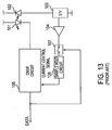
- FIG. 13 illustrates an example of a conventional optical transmitter circuit, including a light emitting element 101 such as a semiconductor laser, a light receiving element 102 such as a photodiode to monitor light, a current-voltage convener (I/V) 103, an auto power control (APC) amplifier 104, a drive circuit 105, a sample hold circuit 106, and an analog switching circuit 107.
- a light emitting element 101 such as a semiconductor laser
- a light receiving element 102 such as a photodiode to monitor light
- I/V current-voltage convener
- APC auto power control
- the drive circuit 105 supplies drive current to the light emitting element 101 in accordance with input data (DATA).
- An optical signal is generated by the light emitting element 101 in accordance with the input data (DATA).
- the optical signal is detected by the monitoring light receiving element 102, converted into voltage by the current-voltage converting circuit 103, and input into the APC amplifier 104.
- the APC amplifier 104 compares the output signal of the current-voltage converting circuit 103 and a reference value, and inputs a signal corresponding to the comparative differential thereof into the sample hold circuit 106 via the analog switching circuit 107.
- the analog switching circuit 107 receives the output signal of the APC amplifier 104 when the data (DATA) converted to optical signals is transmitted at level "1", which output signal is input and held in the sample hold circuit 106.
- the held signal is input into the drive circuit 105 as a current control signal, and the drive current of the light emitting element 101 is controlled so that the optical output remains constant.
- FIGS. 14A-14D are diagrams explaining the operation of the conventional example of the optical transmitter circuit shown in FIG. 13. More specifically, FIG. 14A illustrates the data (DATA) input to the drive circuit 105; FIG. 14B illustrates the optical output signal of the light emitting element 101; FIG. 14C illustrates the output signal of the current-voltage converting circuit 103; and FIG. 14D illustrates the drive current supplied to the light emitting element 101.
- DATA data
- FIG. 14B illustrates the optical output signal of the light emitting element 101
- FIG. 14C illustrates the output signal of the current-voltage converting circuit 103
- FIG. 14D illustrates the drive current supplied to the light emitting element 101.
- the optical output signal is controlled to a specified level, as indicated by the OUTPUT RECOVERY of FIG. 14B.
- a circuit in which stabilization of the optical output is achieved by converting the output current of the light receiving element, which converts the optical output of the light emitting element, into voltage with a current-voltage converting circuit.
- the circuit determines the output to be a significant detection signal, holds it as a sample, and controls the drive current of the light emitting element in accordance with the held value.
- JP9-18054 An example of this type of circuit is disclosed in Japanese Unexamined Laid-Open Patent Application Publication JP9-18054, wherein the input data is delayed and is considered to be a significant detection signal, and the output signal of the current-voltage converting circuit at this time is held as a sample.
- the light emitting element 101 When data (DATA) that is input is increased in speed, e.g., from a low speed of 50 Mbps to 150 Mbps, the light emitting element 101 has sufficient response speed since the light emitting element 101 is generally a semiconductor laser.
- a photodiode is generally used as the light receiving element 102. Because the photodiode has an increased surface area in order to increase the light receiving sensitivity, the capacitance C PD of the photodiode is generally, for example, 20 pF or above.
- the response characteristics are not sufficient to detect an optical signal having a high speed of 150 Mbps or more.
- FIGS. 15A-15D are diagrams illustrating problems occurring with the APC amplifier 104 operation in accordance with the conventional optical transmitter circuit. More specifically, FIG. 15A illustrates the data (DATA) input to the drive circuit 105; FIG. 15B illustrates the optical output signal of the light emitting element 101; FIG. 15C illustrates the output signal of the current-voltage converting circuit 103; and FIG. 15D illustrates the drive current supplied to the light emitting element 101.
- the sample hold circuit 106 samples and holds the output signal of the APC amplifier 104 when the data (DATA) has been input.
- the output signal of the current-voltage converting circuit 103 changes, as shown in FIG. 15C.
- the current control signal corresponding to the value that has been sampled and held is updated at the times t1, t2, t4, and t6, as indicated by the arrows showing the CURRENT UPDATE VALUE in FIG. 15, and the drive current supplied to the light emitting element 101 from the drive circuit 105 is updated. Accordingly, the output signal of the current-voltage converting circuit 103 resulting from the monitoring of the optical output produced by the light receiving element 102 in response to an initial input value of "1" becomes equal to or less than the set value indicated by the broken line at the time t1 in FIG. 15C.
- this output signal of the current-voltage converting circuit 103 is sampled and held, it is judged to be a lower optical output than a specified level, and the drive current supplied to the light emitting element 101 for the next continued data value of "1" increases, as shown in FIG. 15D. Accordingly, the optical output signal of the light emitting element 101 at this time becomes greater than the initial optical output, as shown in FIG. 15B.
- the drive current corresponding to the input data (DATA) "1" is supplied to the light emitting element 101.
- the output signal of the current-voltage converting circuit 103 is lower than the set value at time t4 because of the response speed of the light receiving element 102, as shown in FIG. 15C.
- the drive current with respect to the input data (DATA) "1" at the next time t5 is further increased, as shown in FIG. 15D.
- an optical transmitter circuit comprising a light emitting element to convert input data to an optical output; a light receiving element to receive the optical output of the light emitting element and to output a current corresponding to the optical output; a current-voltage converting circuit to convert the output current of the light receiving element into a voltage and to output a voltage signal; an APC amplifier to compare the output voltage signal of the current-voltage converting circuit and a reference signal and to output a differential output signal; a hold circuit to hold the output signal of the APC amplifier and to form a current control signal; a drive circuit to receive the current control signal from the hold circuit and to supply drive current to the light emitting element in accordance with the current control signal; and a "1" continuous signal detecting circuit to detect a specified number of continuous of "1" bits in the input data and to perform an updating operation on the output signal of the amplifier held in the hold circuit.
- the hold circuit may comprise an analog switching circuit to receive the output signal of the amplifier and a detection signal of the "1" continuous signal detecting circuit, and to switch on in response to the "1" continuous signal detecting circuit detecting the specified number of continuous "1" bits; and a peak detecting circuit to detect and hold a peak value of the output signal of the AC amplifier that is input via the analog switching circuit.
- the optical transmitter circuit may further comprise a peak detecting circuit to detect a peak value of the output signal of the current-voltage converting circuit and to input the peak value to the amplifier.
- the optical transmitter circuit may further comprise a first peak detecting circuit to detect a peak value of the output signal of the current-voltage converting circuit and to output the peak value to the amplifier; and a second peak detecting circuit to detect a peak value of the input data and to output the peak value of the input data to the amplifier as a reference value.
- the hold circuit may comprise an up/down counter to count up or down corresponding to an output signal of the amplifier, in response to the "1" continuous signal detecting circuit detecting the specified number of continuous "1" bits; and a D/A converter to convert the contents of the count of the up/down counter to an analog signal and to input the contents of the count of the up/down counter to the drive circuit as an analog current control signal.
- an optical transmitter circuit comprising a light emitting element to convert input data into an optical output; a light receiving element to receive the optical output of the light emitting element and to output a current corresponding to the optical output; a current-voltage converting circuit to convert the output current of the light receiving element into a voltage and to output a voltage signal; a light deterioration detecting comparator to detect deterioration in the light emitting element by comparing the output signal of the current-voltage converting circuit with a reference value and to output a deterioration detection signal; a "1" continuous signal detecting circuit to detect a specified number of continuous "1" bits in the input data; and a flip-flop to hold the deterioration detection signal from the light deterioration detection comparator in accordance with the detection signal from the "1" continuous signal detecting circuit.
- stabilization of the optical output of the light emitting element and detection of deterioration of the light emitting element can be performed. Furthermore, in accordance with embodiments of the present invention, stabilization of the hold value of the hold circuit or evaluation of light emitting element deterioration is performed by delaying the detection signal from the "1" continuous signal detecting circuit by a delay circuit.
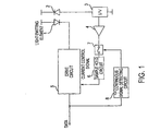
- FIG. 1 is a block diagram of an optical transmitter in accordance with a first embodiment of the present invention.
- the optical transmitter includes a light emitting element 1 such as a semiconductor laser, a light receiving element 2 such as a photodiode, a current-voltage converting circuit (I/V) 3, an APC amplifier 4, a drive circuit 5, a sample hold circuit 6, an analog switching circuit 7, and a "1" continuous signal detecting circuit 8.
- a light emitting element 1 such as a semiconductor laser
- a light receiving element 2 such as a photodiode
- I/V current-voltage converting circuit
- the light receiving element 2 is a photodiode to monitor the output current of the light emitting element 1.
- the light receiving element 2 is preferably a photodiode which does not have a small capacitance.
- the capacitance of the light receiving element 2 photodiode may be 20 pF, or approximately 20 pF.
- the monitored output of the light emitting element 1 produced by the light receiving element 2 is a current which is converted to voltage by the current-voltage converting circuit 3.
- the voltage output by the current-voltage converting circuit 3 is then compared with a reference value by the APC amplifier 4, and the differential output signal of the APC amplifier 4 is input to the sample hold circuit 6 via the analog switching circuit 7.
- the value held by the sample hold circuit 6 is then input to the drive circuit 5 as a current control signal. Furthermore, the "1" continuous signal detecting circuit 8 detects the continuation of a bit value of "1" in the data (DATA) input to the drive circuit 5. When it is detected that several "1" bits have been generated continuously, the analog switching circuit 7 is switched on, and the output signal of the APC amplifier 4 is input and held in the sample hold circuit 6.
- the monitored output of the light receiving element 2 is also gradually increased to a specified value.
- the continuous number of "1" bits that is detected to increase the output of the light receiving element 2 to the specified value is a predetermined number set in advance, and the output signal of the APC amplifier 4 when "1" has been detected in the predetermined number of continuous bits is held in the sample hold circuit 6.
- the stabilization of the optical output can be achieved in accordance with the output signal of the APC amplifier 4. Moreover, if the hold value of the sample hold circuit 6 falls below a set value, it can be determined that there has been deterioration in the light emitting element 1.
- a default value is set as an initial status of the sample hold circuit 6, and a default value of the current control signal can thereby be input to the drive circuit 5.
- the default value can be updated by a continuous "1" bit detection, as described above.
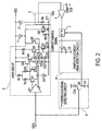
- FIG. 2 is a circuit diagram of the optical transmitter in accordance with the first embodiment of the present invention.
- Q1 through Q9 are field effect transistors (FETs), and Q7 and Q8 represent depression type field effect transistors.
- FETs field effect transistors
- C1 and C2 are capacitors
- D1 through D7 are diodes
- R1 through R6 are resistors
- CI1 through CI4 are constant-current supplies
- V DD and V SS are power voltage
- V REF is a reference voltage
- G1 a complementary output gate circuit.
- the current-voltage converting circuit 3 is comprised of a resistor R6.
- the output current of the light receiving element 2 corresponding to the optical output of the light emitting element 1 is converted to voltage by the resistor R6, input to the APC amplifier 4, and compared with the reference voltage V REF .
- the differential output signal of the APC amplifier 4 is input to the sample hold circuit 6 via the analog switching circuit 7.
- the sample hold circuit 6 is preferably a peak detection circuit comprising a diode D7 and capacitor C2.
- the sample hold circuit 6 inputs the terminal voltage of the capacitor C2 to the gate of the transistor Q7 of the drive circuit 5 as a voltage control signal.
- the "1" continuous signal detecting circuit 8 is comprised of a constant-current supply CI4, a transistor Q9, and a capacitor C1.
- the transistor Q9 is switched on in accordance with a "1" bit in the input data (DATA), and the capacitor C1 is charged from the constant current supply CI4.
- Transistor Q9 is switched off in accordance with "0" bit in the input data (DATA).
- the capacitor C1 discharges via analog switching circuit 7, or alternatively via a pathway not shown in the drawing.
- the discharge time constant of the capacitor C1 is set corresponding to the transmission speed of the input data (DATA), and the capacitor C1 is structured to discharge to under a specified value at least within a 1-bit interval of a "0.”
- the terminal voltage of the capacitor C1 exceeds the specified value and is input to the analog switching circuit 7 as a detection signal via a gate circuit or the like (not shown in the figure), thereby switching on the analog switching circuit 7.
- the analog switching circuit 7 comprises a field effect transistor (FET), and the terminal voltage of the capacitor C1 is applied to a gate thereof so that the field effect transistor is switched on when the terminal voltage of the capacitor C1 exceeds a specified level.
- FET field effect transistor
- the "1" continuous signal detecting circuit 8 may also operate such that the terminal voltage of the capacitor C1 is made to exceed the specified value when "1" has continued for three (3) bits or more, and the analog switching circuit 7 is switched on only when "1,' has continued for three (3) bits or more.
- the drive circuit 5 includes a gate circuit G1 into which data (DATA) is input, and output signals from a non-inverted output terminal of the gate circuit G1 are input to the gate of the transistor Q1. Output signals from the inverted output terminal of the gate circuit G1 are input to the gate of the transistor Q2.
- the transistors Q1 and Q2 make up a differential circuit in conjunction with a constant-current supply CI1, which is commonly connected to the source of transistors Q1 and Q2.
- a level conversion circuit formed by transistors Q3 and Q4 and constant-current supplies CI2 and CI3, inputs level-converted signals to the gates of transistors Q5 and Q6, inputs a current control signal to the transistor Q7 which is commonly connected to transistors Q5 and Q6, and controls the current value supplied to the light emitting element 1 via the transistor Q6. Furthermore, the bias current of the light emitting element 1 is applied via the transistor Q8 in accordance with the setting of the resistor R5.
- FIGS. 3A-3D are diagrams explaining the operation of the optical transmitter in accordance with the first embodiment of the present invention. More specifically, FIG. 3A illustrates data (DATA) input to the optical transmitter, FIG. 3B illustrates the optical output signal of the light emitting element 1, FIG. 3C illustrates the output signal of the current-voltage converting circuit 3, and FIG. 3D illustrates the drive current supply to the light emitting element 1.
- FIG. 3A when a "1" bit is input continuously at time t0 and at the following time t1, even when the output signal of the current-voltage converting circuit 3 does not increase to the set value (indicated by the broken line shown in FIG. 3C) because of the response delay of the light receiving element 2, the output signal of the current-voltage converting circuit 3 is able to increase to the set value at the time t2 because of the continuation of "1" for two (2) bits.
- the terminal voltage of the capacitor C1 of the "1" continuous signal detecting circuit 8 exceeds the specified value following time t1.
- the analog switching circuit 7 is thereby switched on, and, as shown as the CURRENT VALUE UPDATE at the time t2, the peak value of the output signal of the APC amplifier 4 is held by the capacitor C2 of the sample hold circuit 6. Accordingly, a drive current roughly equal to the drive current supplied to the data input in the previous times t0 and t1 is supplied to the data input at the following time t3.
- the output signal of the current-voltage converting circuit 3 does not increase to the set level indicated by the broken line at times t4 and t6 because of the slow response characteristics of the light receiving element 2. Moreover, the terminal voltage of the capacitor C1 of the "1" continuous signal detecting circuit 8 does not increase to the specified level, and thereby the analog switching circuit 7 remains off. Accordingly, since the output signal of the APC amplifier 4 corresponding to the excessive output signal of the current-voltage converting circuit 3 is not held, the current value is not updated.
- the analog switching circuit 7 When “1" bits are continuously input, the analog switching circuit 7 is switched on by the "1" continuous signal detecting circuit 8, and the output signal of the APC amplifier 4 can be held in the sample hold circuit 6.
- the sample hold circuit 6 since holding by the sample hold circuit 6 can be performed at the timing indicated as a CURRENT VALUE UPDATE in FIGS. 3A-3D, even in the case of an independent bit input during the time t3 or t5, the drive current of the light emitting element 1 can be controlled so as to obtain a normal optical output.
- the continuous number of "1" bits to be detected is set in accordance with the relationship between the speed of the input data (DATA) and the response characteristics of the light receiving element 2. For example, when “1" has continued for three (3) bits or longer, and a light receiving element 2 having response characteristics which increase to the set value is used, as described above, the "1,' continuous signal detecting circuit 8 may operate so that the analog switching circuit 7 is switched on when three continuous "1" bits have been detected.
- FIG. 4 is a block diagram of an optical transmitter in accordance with a second embodiment of the present invention.
- the optical transmitter shown in FIG. 4 includes a light emitting element 11, such as a semiconductor laser, a light receiving element 12 such as a photodiode, a current-voltage converting circuit (I/V) 13, an APC amplifier 14, a drive circuit15, a sample hold circuit 16, an analog switching circuit 17, a "1" continuous signal detecting circuit 18, and a peak detecting circuit 19 including a capacitor C3 and a diode D8.
- the analog switching circuit 17 is switched on, and the output signal of the APC amplifier 14 is input to the sample hold circuit 16 and held.
- the value held by the sample hold circuit 16 is input to the drive circuit 15 as a current control signal to control the drive current supplied to the light emitting element 11 in accordance with the input data (DATA).
- the optical output of the light emitting element 11 corresponding to the drive current is monitored by the light receiving element 12.
- the peak detecting circuit 19 is provided between the current-voltage converting circuit 13 and the APC amplifier 14.
- the peak detecting circuit 19 detects the peak value of the output signal of the current-voltage converting circuit 13 and inputs the detected peak value to the APC amplifier 14.
- the output signal of the current-voltage converting circuit 13 is temporarily held by the peak detecting on circuit 19. Temporarily holding the output signal of the current-voltage converting circuit 13 stabilizes the output signal of the APC amplifier 14, which is input via the analog switching circuit 17 to the sample hold circuit 16, thereby preventing an operational error when the current control signal that is held in the sample hold circuit 16 is updated.
- FIGS. 5A-5D are diagrams explaining the operation of the optical transmitter in accordance with the second embodiment of the present invention. More specifically, FIG. 5A illustrates the data (DATA) input into the drive circuit 15; FIG. 5B illustrates the output signal of the "1" continuous signal detecting circuit 18; FIG. 5C illustrates the output signal of the peak detecting circuit 19; and FIG. 5D illustrates the drive current applied from the drive circuit 15 to the light emitting element 11.
- DATA data
- FIG. 5B illustrates the output signal of the "1" continuous signal detecting circuit 18
- FIG. 5C illustrates the output signal of the peak detecting circuit 19
- FIG. 5D illustrates the drive current applied from the drive circuit 15 to the light emitting element 11.
- the "1" continuous signal detecting circuit 18 detects two (2) continuous "1" bits, it outputs a detection signal during time t2.
- the analog switching circuit 17 is thus switched on, and the output signal of the peak detecting circuit 19 shown in FIG. 5C at this time is held by the sample hold circuit 16.
- the current control signal is updated with respect to the drive circuit 15. In this case, the peak value of the output signal of the current-voltage converting circuit 13 is held by the peak detecting circuit 19, so that holding in the sample hold circuit 16 can be reliably performed.
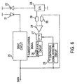
- FIG. 6 is a block diagram of an optical transmitter in accordance with a third embodiment of the present invention.
- the optical transmitter shown in FIG. 6 includes a light emitting element 21 such as a semiconductor laser, a light receiving element 22 such as a photodiode, a current-voltage converting circuit (I/V) 23, an APC amplifier 24, a drive circuit 25, a sample hold circuit 26, an analog switching circuit 27, a "1" continuous signal detecting circuit 28, and peak detecting circuits 29 and 30.
- the peak detecting circuit 29 operates in the same manner as the peak detecting circuit 19 in the third embodiment shown in FIG. 4.
- the peak detection circuit 30 detects the peak values of the input data (DATA) and uses the detected value thereof as the reference value for the APC amplifier 24.
- the error portion of the peak detecting circuit 29 can be offset, and the optical output of the light emitting element 21 can be monitored with better accuracy.
- FIG. 7 is a block diagram of an optical transmitter in accordance with a fourth embodiment of the present invention.
- the optical transmitter in accordance with the fourth embodiment of the invention includes a light emitting element 31 such as a semiconductor laser, a light receiving element 32 such as a photodiode, a current-voltage converting circuit (I/V) 33, an APC amplifier 34, a drive circuit 35, a sample hold circuit 36 which includes an analog switch circuit, a "1" continuous signal detecting circuit 38, a peak detecting circuit 39, and a delay circuit 40.
- the fourth embodiment of the present invention is similar to the third embodiment of the invention shown in FIG. 4 and further includes the delay circuit 40 between the "1" continuous signal detecting circuit 38 and the analog switch circuit 36.
- the delay circuit 40 is also applicable to the embodiments of the invention shown in FIG. 1 and FIG. 6.
- the delay circuit 40 may, for example, be a delay circuit as shown in FIG. 8. However, various other types of delay circuits may be used.
- the delay circuit 40 is preferably a shift register including a plurality of flip-flops 41-1 through 41-n which are vertically connected, with a clock signal CLK input to the respective clock terminals C of each flip-flop 41-1 through 41-n, and a detection signal from the "1" continuous signal detecting circuit 38 input to the data terminal D of the initial flip-flop 41-1.
- the delay time of the shift register delay circuit 40 can be selected in accordance with the speed of the clock signal CLK and the number of connections of the flip-flops 41-1 though 41-n.
- the output signal of the current-voltage converting circuit 33 is input to the peak detecting circuit 39 and its peak value is detected.
- FIG. 5C there is a deviation in the time until the set value indicated by the broken line is reached, and there is also deviation in the timing at which two (2) continuous "1" bits are detected in the case of the embodiment shown in FIG. 2.
- the "1" continuous detection signal is delayed by the delay circuit 40 until the output signal of the current-voltage converting circuit 33 corresponding to the optical output by the light emitting element 31 is obtained.
- the output signal of the peak detecting circuit 39 has been stabilized, the output signal of the APC amplifier 34 is held in the sample hold circuit 36 and is used as a current control signal that is input to the drive circuit 35.
- the operation of the other elements shown in FIG. 7 is similar to the operation of like elements in the embodiments described above, and an explanation of these like elements will not be repeated here.
- FIG. 9 is a block diagram of an optical transmitter in accordance with a fifth embodiment of the present invention.
- the optical transmitter includes a light emitting element 51 such as a semiconductor laser, a light receiving element 52 such as a photodiode, a current-voltage converting circuit (I/V) 53, an APC amplifier 54, a drive circuit 55, a digital hold circuit 56, an up/down counter (U/D) 57, a "1" continuous signal detecting circuit 58, a peak detecting circuit 59, and a digital-to-analog (D/A) converter 60.
- a light emitting element 51 such as a semiconductor laser
- a light receiving element 52 such as a photodiode
- I/V current-voltage converting circuit
- APC amplifier 54 an APC amplifier 54
- drive circuit 55 a digital hold circuit 56
- U/D up/down counter
- U/D up/down counter
- a "1" continuous signal detecting circuit 58 a peak detecting circuit
- the digital hold circuit 56 which corresponds to the sample hold circuit in the above-described embodiments, comprises the up/down counter 57 and the D/A converter 58. As shown in FIG. 9, the detection signal from the "1" continuous signal detecting circuit 58 is used as an enable signal of the up/down counter 57. An up-count or a down-count is performed in correspondence to the output signal of the APC amplifier 54 when, for example, two (2) continuous "1" bits are detected in the input data (DATA).
- DATA input data
- the output signal of the APC amplifier 54 causes the up/down counter 57 to count down, while the up/down counter 57 counts up in accordance with the output signal of the APC amplifier 54 when the output signal of the peak detecting circuit 59 is lower than the reference value.
- the up/down counter 57 counts down when the optical output of the light emitting element 51 exceeds a set value, and counts up when the optical output of the light emitting element 51 is lower than the set value.
- the optical output of the light emitting element 51 can be controlled to be a set value.
- FIG. 10 is a diagram explaining the "1" continuous signal detecting circuit in accordance with embodiments of the present invention.
- the "1" continuous signal detecting circuit is a shift register is comprising of a plurality of vertically connected flip-flops 61-1 through 61-n.
- a clock signal CLK is input to respective clock terminals C of the flip-flops 61-1 through 61-n
- input data (DATA) is input into a data terminal D of the initial flip-flop 61-1
- the output signal Q of each respective flip-flop 61-1 through 61-n is input into an AND circuit 62.
- the two flip-flops 61-1 and 61-2 are used in the "1" continuous bit detecting circuit, since the output terminals Q of the flip-flops 61-1 and 61-2 are both “1" because of the two continuous "1” bits, the output of the AND circuit 62 becomes “1.” In other words, in the case of two (2) or more continuous "1” bits, continuous "1" detection signals are obtained. When a "0" bit is input, the output signal of the AND circuit 62 becomes "0.”
- Counting up or counting down by the up/down counter 57 is performed using the detection signal of the "1" continuous bit detecting circuit as the enable signal of the up/down counter 57. Furthermore, when three (3) or more continuous "1" bits are detected, three or more vertically connected flip-flops can be used.
- the "1" continuous signal detecting circuit shown in FIG. 10 can also be used as the "1" continuous signal detecting circuits 8, 18, 28, and 38 in the embodiments described above.
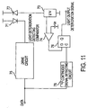
- FIG. 11 is a block diagram of an optical transmitter in accordance with a sixth embodiment of the present invention.
- the optical transmitter includes a light emitting element 71 such as a semiconductor laser, a light receiving element 72 such as a photodiode, a current-voltage converting circuit (I/V) 73, a comparator 74 to detect light deterioration, a drive circuit 75, a flip-flop 76, and a "1" continuous signal detecting circuit 78.
- the optical output of the light emitting element 71 is monitored by the light receiving element 72, and, when the optical output does not reach the desired optical output even when the drive current from the drive circuit 75 is controlled, it is judged that deterioration of the light emitting element 71 has occurred.
- an inexpensive photodiode having response characteristics that are unable to follow the optical output of the light emitting element 71 is used as the light receiving element 72, even if the optical output corresponding to one isolated "1" bit in the input data (DATA) is monitored, the output signal of the current-voltage converting circuit 73 does not rise to the specified value, as described with reference to FIG. 3 and FIG. 5. Therefore, there is a possibility that the light emitting element 71 will be judged to have deteriorated.
- the output signal of the current-voltage converting circuit 73 which converts the output current of the light receiving element 72 to voltage, and the reference value Vr input to the light deterioration detecting comparator 74, are compared.
- a comparison output signal of "0" is input into the data terminal D of the flip-flop 76 when the output value of the current-voltage converting circuit 73 exceeds the reference value Vr, and a “1” is input to the data terminal D of the flip-flop 76 when the output value of the current-voltage converting circuit 73 is lower than the reference value Vr.
- the detection signal of the "1" continuous signal detecting circuit 78 is input to the clock terminal C of the flip-flop 76.
- the output signal of the current-voltage converting circuit 73 does not rise to the specified level in the case where the input data (DATA) is an independent "1" bit. Further, even if a "1" signal indicating deterioration is output from the light deterioration detecting comparator 74, because the flip-flop 76 is not set, an optical output deterioration signal is not produced.
- the drive circuit 75 may be any of various types of drive circuits. Further, when the response characteristics of the light receiving element 72 are relatively slow, the "1" continuous signal detecting circuit 78 can be designed to operate to determine whether or not there is deterioration of the light emitting element 71 when three continuous "1" bits are detected.
- FIG. 12 is a block diagram of an optical transmitter in accordance with a seventh embodiment of the present invention.
- the optical transmitter includes a light emitting element 81 such as a semiconductor laser, a light receiving element 82 such as a photodiode, a current-voltage converting circuit (I/V) 83, a comparator to detect optical deterioration 84, a drive circuit 85, a sample hold circuit 86, a "1" continuous signal detecting circuit 88, peak detecting circuits 89 and 90, a comparator 91 to detect optical deterioration, and a flip-flop 92.
- a light emitting element 81 such as a semiconductor laser
- a light receiving element 82 such as a photodiode
- I/V current-voltage converting circuit
- the peak detecting circuit 90, the comparator 91 to detect optical deterioration, and the flip-flop 92 are provided in addition to the elements shown in the embodiment of FIG. 4, allowing the deterioration of the light emitting element 81 to be detected thereby. Furthermore, the monitoring of the optical output of the light emitting element 81 by the light receiving element 82, and the controlling of the drive circuit 85 in accordance with a current control signal so that the optical output remains constant, are performed in a manner similar to the embodiments shown in FIG. 1, FIG. 4, FIG. 6, and FIG. 7, and an explanation of these elements and their associated functions will not be repeated here.
- the peak value of the output signal of the current-voltage converting circuit 83 is detected by the peak detecting circuit 90 and is compared with a reference value Vr by the optical deterioration detecting comparator 91 in a stabilized state.
- a "1” indicating deterioration of the light emitting element 81 is output, and otherwise a "0" is output.
- a continuous "1” is not detected in the input data (DATA) by the "1" continuous signal detecting circuit 88, deterioration evaluation is not performed.
- embodiments of the present invention may operate such that the output signal of the current-voltage converting circuit is converted into a digital signal which undergoes digital processing.
- a conventional photodiode having a comparatively large capacity can be used as the light receiving element to monitor the light emitting element, such as a semiconductor laser or light emitting diode. More specifically, by using the detection of continuous "1" bits from the "1" continuous signal detection circuit, an update timing of the current control signal or a deterioration evaluation timing of the light emitting element can be performed. Accordingly, the advantage of cost reduction in the light transferring circuit can be achieved.
Landscapes
- Physics & Mathematics (AREA)
- Electromagnetism (AREA)
- Engineering & Computer Science (AREA)
- Computer Networks & Wireless Communication (AREA)
- Signal Processing (AREA)
- Optics & Photonics (AREA)
- Optical Communication System (AREA)
- Dc Digital Transmission (AREA)
- Semiconductor Lasers (AREA)
Abstract
Description
Claims (19)
- An optical transmitter circuit, comprising:a light emitting element to convert input data into an optical output;a light receiving element to receive the optical output of the light emitting element and to output a current corresponding to the optical output;a current-voltage converting circuit to convert the output current of the light receiving element into a voltage and to output a voltage signal;an amplifier to compare the output voltage signal of the current-voltage converting circuit and a reference signal and to output a differential output signal;a hold circuit to hold the output signal of the amplifier and to form a current control signal;a drive circuit to receive the current control signal from the hold circuit and to supply drive current to the light emitting element in accordance with the current control signal; anda "1" continuous signal detecting circuit to detect a specified number of continuous "1" bits in the input data and to perform an updating operation on the output signal of the amplifier held in the hold circuit.
- An optical transmitter circuit as recited in claim 1, wherein the hold circuit comprises:an analog switching circuit to receive the output signal of the amplifier and a detection signal of the "1" continuous signal detecting circuit, and to switch on in response to the "1" continuous signal detecting circuit detecting the specified number of continuous "1" bits; anda peak detecting circuit to detect and hold a peak value of the output signal of the amplifier that is input via the analog switching circuit.
- An optical transmitter circuit as recited in claim 1, further comprising a peak detecting circuit to detect a peak value of the output signal of the current-voltage converting circuit and to input the peak value to the amplifier.
- An optical transmitter circuit as recited in claim 1, further comprising:a first peak detecting circuit to detect a peak value of the output signal of the current-voltage converting circuit and to output the peak value to the amplifier; anda second peak detecting circuit to detect a peak value of the input data and to output the peak value of the input data to the amplifier as a reference value.
- An optical transmitter circuit as recited in claim 1, wherein the hold circuit comprises:an up/down counter to count up or down corresponding to an output signal of the amplifier, in response to the "1" continuous signal detecting circuit detecting the specified number of continuous "1" bits; anda D/A converter to convert the contents of the count of the up/down counter to an analog signal and to input the contents of the count of the up/down counter to the drive circuit as an analog current control signal.
- An optical transmitter circuit as recited in claim 5, wherein the up/down counter counts down in response to the output of the light emitting element exceeding a set value and counts up in response to the output of the light emitting element being lower than the set value.
- An optical transmitter circuit, comprising:a light emitting element to convert input data into an optical output;a light receiving element to receive the optical output of the light emitting element and to output a current corresponding to the optical output;a current-voltage converting circuit to convert the output current of the light receiving element into a voltage;a light deterioration detecting comparator to detect deterioration in the light receiving element by comparing the output signal of the current-voltage converting circuit with a reference value and to output a deterioration detection signal;a "1" continuous signal detecting circuit to detect a specified number of continuous "1" bits in the input data and to output a detection signal; anda flip-flop to hold the deterioration detection signal from the light deterioration detection comparator in accordance with the detection signal from the "1" continuous signal detecting circuit.
- An optical transmitter circuit as recited in claim 7, further comprising:an amplifier to receive the output voltage of the current-voltage converting circuit;a drive circuit to drive the light emitting element; anda hold circuit to hold the output signal of the amplifier in accordance with the detection signal from the "1" continuous signal detecting circuit and to input a current control signal to the drive circuit of the light emitting element.
- An optical transmitter circuit as recited in claim 8, further comprising a delay circuit to delay the detection signal from the "1" continuous signal detecting circuit and to input the delayed detection signal to the hold circuit and flip-flop.
- An optical transmitter including a light emitting element to convert input data to an optical output, comprising:a current controller to detect a predetermined number of continuous bits of the same type in the input data, to generate a detection signal in response to detecting the predetermined number of bits, and to generate a drive current supplied to the light emitting element in accordance with the detection signal.
- An optical transmitter including a light emitting element to convert input data to an optical output, comprising:a current generator to generate a drive current to drive the light emitting element;a continuous signal detecting circuit to detect a predetermined number of continuous "1" bits in the input data and to output a control signal to the current generator to control the drive current in response to detecting the predetermined number of "1" bits.
- An optical transmitter as recited in claim 11, wherein the predetermined number of "1" bits is set in accordance with a relationship between a speed of the input data and a response characteristic of the light emitting element.
- An optical transmitter as recited in claim 11, wherein the predetermined number of continuous "1" bits is two.
- An optical transmitter as recited in claim 11, wherein the current generator comprises:a light receiving element to receive the optical output of the light emitting element and to output a current corresponding to the optical output;a current-voltage converting circuit to convert the output current of the light receiving element into a voltage and to output a voltage signal;a drive circuit to supply drive current to the light emitting element;a current control signal generator to receive the voltage signal output by the current-voltage converting circuit and the control signal output by the continuous signal detecting circuit and to generate a current control signal to control the drive current supplied to the light emitting element by the drive circuit.
- An optical transmitter as recited in claim 14, wherein the current control signal generator includes a switching circuit, and the control signal output by the continuous signal detecting circuit controls switching of the switching circuit to update the current control signal.
- An optical transmitter as recited in claim 14, wherein the current control signal generator includes an up/down counter to count up or down in response to the control signal generated by the continuous signal detecting circuit, wherein a count of the up/down counter controls the drive current.
- An optical transmitter as recited in claim 15, wherein the current control signal generator further comprises a delay circuit between the continuous signal detecting circuit and the switching circuit to the control signal from the continuous signal detecting circuit.
- An optical transmitter as recited in claim 15, wherein the current controller comprises:a comparator to compare the output voltage signal of the current-voltage converting circuit and a reference signal and to output a difference signal; anda sample and hold circuit to receive the difference signal output by the comparator in response to the switching circuit being switched on, to hold the difference signal output by the comparator, and to input the held difference signal to the drive circuit as the current control signal.
- An optical transmitter, comprising:a light emitting element to convert input data into an optical output;a light deterioration detector to detect deterioration in the light receiving element; anda continuous signal detector to detect a predetermined number of continuous "1" bits in the input data and to output a detection signal indicating that the predetermined number of continuous "1" bits have been detected,
wherein the light deterioration detector outputs a signal indicating whether deterioration has occurred in response to the detection signal.
Applications Claiming Priority (2)
| Application Number | Priority Date | Filing Date | Title |
|---|---|---|---|
| JP7502599 | 1999-03-19 | ||
| JP11075025A JP2000269898A (en) | 1999-03-19 | 1999-03-19 | Optical transmission circuit |
Publications (2)
| Publication Number | Publication Date |
|---|---|
| EP1039665A2 true EP1039665A2 (en) | 2000-09-27 |
| EP1039665A3 EP1039665A3 (en) | 2004-11-10 |
Family
ID=13564240
Family Applications (1)
| Application Number | Title | Priority Date | Filing Date |
|---|---|---|---|
| EP00101267A Withdrawn EP1039665A3 (en) | 1999-03-19 | 2000-01-26 | Optical transmitter circuit |
Country Status (3)
| Country | Link |
|---|---|
| US (1) | US6597485B1 (en) |
| EP (1) | EP1039665A3 (en) |
| JP (1) | JP2000269898A (en) |
Cited By (3)
| Publication number | Priority date | Publication date | Assignee | Title |
|---|---|---|---|---|
| US7420906B2 (en) * | 2002-09-11 | 2008-09-02 | Samsung Electronics Co., Ltd. | Automatic power calibration apparatus for optical recording device and automatic power calibration method therefor |
| CN106330323A (en) * | 2016-09-18 | 2017-01-11 | 青岛海信宽带多媒体技术有限公司 | OLT optical module and OLT |
| WO2021051676A1 (en) * | 2019-09-20 | 2021-03-25 | 武汉光迅科技股份有限公司 | Drive circuit for direct modulated laser, and direct modulated optical transmitter |
Families Citing this family (17)
| Publication number | Priority date | Publication date | Assignee | Title |
|---|---|---|---|---|
| US7376351B2 (en) * | 2000-10-24 | 2008-05-20 | Geberit Technik Ag | Data communications system and method for communication between infrared devices |
| US7203213B2 (en) * | 2003-12-15 | 2007-04-10 | Micrel, Incorporated | Laser turn-on accelerator independent of bias control loop bandwidth |
| US7532653B2 (en) * | 2004-01-15 | 2009-05-12 | Micrel, Inc. | Laser turn-on accelerator independent of bias control loop bandwidth |
| US7505496B2 (en) * | 2006-04-05 | 2009-03-17 | Ciena Corporation | Systems and methods for real-time compensation for non-linearity in optical sources for analog signal transmission |
| JP5292808B2 (en) * | 2007-12-28 | 2013-09-18 | 株式会社リコー | Semiconductor laser driving device and image forming apparatus including the semiconductor laser driving device |
| US8693878B2 (en) * | 2008-12-04 | 2014-04-08 | Koninklijke Philips N.V. | Illumination device and method for embedding a data signal in a luminance output using AC driven light sources |
| US8155536B2 (en) * | 2008-12-31 | 2012-04-10 | Intel Corporation | Optical transceiver IC |
| CN101594184B (en) * | 2009-06-11 | 2012-04-11 | 青岛海信宽带多媒体技术有限公司 | Optical line terminal |
| US9300405B2 (en) * | 2011-12-02 | 2016-03-29 | Semtech Corporation | Closed loop optical modulation amplitude control |
| US10097908B2 (en) * | 2014-12-31 | 2018-10-09 | Macom Technology Solutions Holdings, Inc. | DC-coupled laser driver with AC-coupled termination element |
| US10630052B2 (en) | 2017-10-04 | 2020-04-21 | Macom Technology Solutions Holdings, Inc. | Efficiency improved driver for laser diode in optical communication |
| EP3804247B1 (en) | 2018-05-30 | 2024-08-14 | MACOM Technology Solutions Holdings, Inc. | Integrated circuit based ac coupling topology |
| US11005573B2 (en) | 2018-11-20 | 2021-05-11 | Macom Technology Solutions Holdings, Inc. | Optic signal receiver with dynamic control |
| US12013423B2 (en) | 2020-09-30 | 2024-06-18 | Macom Technology Solutions Holdings, Inc. | TIA bandwidth testing system and method |
| US11658630B2 (en) | 2020-12-04 | 2023-05-23 | Macom Technology Solutions Holdings, Inc. | Single servo loop controlling an automatic gain control and current sourcing mechanism |
| US12395130B2 (en) | 2022-12-27 | 2025-08-19 | Macom Technology Solutions Holdings, Inc. | Variable gain optical modulator with open collector driver amplifier and method of operation |
| US12567847B2 (en) | 2022-12-27 | 2026-03-03 | Macom Technology Solutions Holdings, Inc. | Variable gain optical modulator with open collector driver amplifier and method of operation |
Family Cites Families (12)
| Publication number | Priority date | Publication date | Assignee | Title |
|---|---|---|---|---|
| US4201907A (en) * | 1977-08-29 | 1980-05-06 | International Totalizing Systems, Inc. | Totalizer system |
| CA1186763A (en) * | 1981-04-20 | 1985-05-07 | Masami Kato | Consecutive identical digit suppression system in a digital communication system |
| US4856011A (en) * | 1985-01-30 | 1989-08-08 | Ricoh Company, Ltd. | Semiconductor laser control circuit |
| JPS6448480A (en) * | 1987-08-19 | 1989-02-22 | Fujitsu Ltd | Semiconductor laser modulation control system |
| US4856008A (en) * | 1987-12-29 | 1989-08-08 | Ricoh Company, Ltd. | Semiconductor laser control apparatus |
| JP2815183B2 (en) * | 1989-08-01 | 1998-10-27 | 株式会社リコー | Laser beam scanning position detector |
| US5060302A (en) * | 1990-02-28 | 1991-10-22 | At&T Bell Laboratories | Automatic adjustment of optical power output of a plurality of optical transmitters |
| US5390041A (en) * | 1991-11-06 | 1995-02-14 | Cray Research, Inc. | Fiber optic channel extender interface method and apparatus |
| JP3231436B2 (en) * | 1992-11-16 | 2001-11-19 | 旭光学工業株式会社 | Optical output switching device of laser light emitting device |
| JP2842762B2 (en) * | 1993-06-30 | 1999-01-06 | シャープ株式会社 | Infrared data transfer device |
| US5978124A (en) * | 1995-04-28 | 1999-11-02 | Mitsubishi Denki Kabushiki Kaisha | Light emitting control apparatus and optical transmitter |
| JP3839577B2 (en) * | 1998-03-11 | 2006-11-01 | 富士通株式会社 | Semiconductor laser drive circuit |
-
1999
- 1999-03-19 JP JP11075025A patent/JP2000269898A/en not_active Withdrawn
-
2000
- 2000-01-26 EP EP00101267A patent/EP1039665A3/en not_active Withdrawn
- 2000-03-03 US US09/517,621 patent/US6597485B1/en not_active Expired - Fee Related
Cited By (6)
| Publication number | Priority date | Publication date | Assignee | Title |
|---|---|---|---|---|
| US7420906B2 (en) * | 2002-09-11 | 2008-09-02 | Samsung Electronics Co., Ltd. | Automatic power calibration apparatus for optical recording device and automatic power calibration method therefor |
| CN106330323A (en) * | 2016-09-18 | 2017-01-11 | 青岛海信宽带多媒体技术有限公司 | OLT optical module and OLT |
| US10110316B2 (en) | 2016-09-18 | 2018-10-23 | Hisense Broadband Multimedia Technologies Co., Ltd. | OLT optical module and OLT |
| CN106330323B (en) * | 2016-09-18 | 2019-01-08 | 青岛海信宽带多媒体技术有限公司 | OLT optical module and OLT |
| WO2021051676A1 (en) * | 2019-09-20 | 2021-03-25 | 武汉光迅科技股份有限公司 | Drive circuit for direct modulated laser, and direct modulated optical transmitter |
| US12334708B2 (en) | 2019-09-20 | 2025-06-17 | Accelink Technologies Co., Ltd. | Drive circuit for direct modulated laser, and direct modulated optical transmitter |
Also Published As
| Publication number | Publication date |
|---|---|
| JP2000269898A (en) | 2000-09-29 |
| EP1039665A3 (en) | 2004-11-10 |
| US6597485B1 (en) | 2003-07-22 |
Similar Documents
| Publication | Publication Date | Title |
|---|---|---|
| EP1039665A2 (en) | Optical transmitter circuit | |
| EP1039666B1 (en) | Burst mode optical transmitter circuit | |
| US5923219A (en) | Automatic threshold control circuit and signal amplifying circuit for amplifying signals by compensating for low-frequency response of photodetector | |
| US6118829A (en) | Apparatus and method for automatic mode selection in a communications receiver | |
| US8238395B2 (en) | Automatic power control (APC) loop for adjusting the bias current of a laser diode | |
| US7266308B2 (en) | Light output control circuit | |
| US6597245B2 (en) | Preamplifier | |
| KR100270757B1 (en) | Voltage monitoring circuit and voltage monitoring method with hysteresis characteristic | |
| US5914484A (en) | Circuit for adjusting luminous energy of light-emitting element and optical device using same | |
| US20020063937A1 (en) | Optical receiving apparatus | |
| EP1717972B1 (en) | Automatic bit rate control circuit | |
| US4801788A (en) | Bar code scanner for a video signal which has a shading waveform | |
| US6982408B2 (en) | Photo-detecting method and photo-detecting device with varying modulation frequency | |
| US6480311B1 (en) | Peak-hold circuit and an infrared communication device provided with such a circuit | |
| US6377108B1 (en) | Low jitter differential amplifier with negative hysteresis | |
| US7652508B2 (en) | Circuit device and electronic equipment provided with the same | |
| US20030095315A1 (en) | Apparatus for detecting cutoff of optical signal, optical receiver, optical transmitter, and method of detecting cutoff of optical signal | |
| US8405429B2 (en) | Power supply voltage monitor circuit | |
| US6188264B1 (en) | Automatic threshold level control circuit | |
| US20060139736A1 (en) | Optical receiver | |
| US20020057480A1 (en) | Optical receiver for optical communications | |
| EP1199799A2 (en) | Signal compensator circuit and demodulator circuit | |
| US6728495B1 (en) | Light output control circuit with a warning function of deteriorated light output | |
| US5075542A (en) | Photoelectric switch using pulse width discrimination | |
| US20050128007A1 (en) | Preamplifier circuit, clock switching circuit, and optical receiver |
Legal Events
| Date | Code | Title | Description |
|---|---|---|---|
| PUAI | Public reference made under article 153(3) epc to a published international application that has entered the european phase |
Free format text: ORIGINAL CODE: 0009012 |
|
| AK | Designated contracting states |
Kind code of ref document: A2 Designated state(s): AT BE CH CY DE DK ES FI FR GB GR IE IT LI LU MC NL PT SE |
|
| AX | Request for extension of the european patent |
Free format text: AL;LT;LV;MK;RO;SI |
|
| PUAL | Search report despatched |
Free format text: ORIGINAL CODE: 0009013 |
|
| AK | Designated contracting states |
Kind code of ref document: A3 Designated state(s): AT BE CH CY DE DK ES FI FR GB GR IE IT LI LU MC NL PT SE |
|
| AX | Request for extension of the european patent |
Extension state: AL LT LV MK RO SI |
|
| AKX | Designation fees paid | ||
| REG | Reference to a national code |
Ref country code: DE Ref legal event code: 8566 |
|
| STAA | Information on the status of an ep patent application or granted ep patent |
Free format text: STATUS: THE APPLICATION IS DEEMED TO BE WITHDRAWN |
|
| 18D | Application deemed to be withdrawn |
Effective date: 20050511 |