EP1039530A2 - Method for manufacturing semiconductor device capable of avoiding flaws and erosion caused by metal chemical-mechanical polishing process - Google Patents
Method for manufacturing semiconductor device capable of avoiding flaws and erosion caused by metal chemical-mechanical polishing process Download PDFInfo
- Publication number
- EP1039530A2 EP1039530A2 EP00104654A EP00104654A EP1039530A2 EP 1039530 A2 EP1039530 A2 EP 1039530A2 EP 00104654 A EP00104654 A EP 00104654A EP 00104654 A EP00104654 A EP 00104654A EP 1039530 A2 EP1039530 A2 EP 1039530A2
- Authority
- EP
- European Patent Office
- Prior art keywords
- layer
- set forth
- sacrifice
- forming
- conductive layer
- Prior art date
- Legal status (The legal status is an assumption and is not a legal conclusion. Google has not performed a legal analysis and makes no representation as to the accuracy of the status listed.)
- Withdrawn
Links
Images












Classifications
-
- H—ELECTRICITY
- H10—SEMICONDUCTOR DEVICES; ELECTRIC SOLID-STATE DEVICES NOT OTHERWISE PROVIDED FOR
- H10W—GENERIC PACKAGES, INTERCONNECTIONS, CONNECTORS OR OTHER CONSTRUCTIONAL DETAILS OF DEVICES COVERED BY CLASS H10
- H10W20/00—Interconnections in chips, wafers or substrates
- H10W20/01—Manufacture or treatment
- H10W20/031—Manufacture or treatment of conductive parts of the interconnections
- H10W20/056—Manufacture or treatment of conductive parts of the interconnections by filling conductive material into holes, grooves or trenches
- H10W20/058—Manufacture or treatment of conductive parts of the interconnections by filling conductive material into holes, grooves or trenches by depositing on sacrificial masks, e.g. using lift-off
-
- H—ELECTRICITY
- H10—SEMICONDUCTOR DEVICES; ELECTRIC SOLID-STATE DEVICES NOT OTHERWISE PROVIDED FOR
- H10P—GENERIC PROCESSES OR APPARATUS FOR THE MANUFACTURE OR TREATMENT OF DEVICES COVERED BY CLASS H10
- H10P52/00—Grinding, lapping or polishing of wafers, substrates or parts of devices
- H10P52/40—Chemomechanical polishing [CMP]
- H10P52/403—Chemomechanical polishing [CMP] of conductive or resistive materials
-
- H—ELECTRICITY
- H10—SEMICONDUCTOR DEVICES; ELECTRIC SOLID-STATE DEVICES NOT OTHERWISE PROVIDED FOR
- H10W—GENERIC PACKAGES, INTERCONNECTIONS, CONNECTORS OR OTHER CONSTRUCTIONAL DETAILS OF DEVICES COVERED BY CLASS H10
- H10W20/00—Interconnections in chips, wafers or substrates
- H10W20/01—Manufacture or treatment
- H10W20/031—Manufacture or treatment of conductive parts of the interconnections
- H10W20/062—Manufacture or treatment of conductive parts of the interconnections by smoothing of conductive parts, e.g. by planarisation
Definitions
- the present invention relates to a method for manufacturing a semiconductor device capable of avoiding flaws or scratches and erosion caused by a metal chemical mechanical polishing ("metal CMP") process.
- metal CMP metal chemical mechanical polishing
- CMP processes are popularly used in planarizing interlayers or insulating layers of semiconductor devices. This is because miniaturized semiconductor devices are required to be perfectly planarized as the exposure margin is reduced as a result of the design rules adapted to the semiconductor devices that require beams of light with a shorter wavelength for exposure in order to obtain finer patterns. Such CMP processes are called "oxide CMP" processes.
- CMP processes are used to planarize metal layers made of tungsten (W), aluminum (Al) or copper (Cu) buried in plug holes or grooves in order to prepare semiconductor devices showing a quality level higher than those prepared by conventional etching back processes. These CMP processes are called "metal CMP" processes.
- the "metal CMP" processes are applied to a damascene method for forming a wiring layer and a dual-damascene method for forming a plug and a wiring layer on the plug at the same time.
- CMP processes are indispensable for the manufacture of high performance semiconductor devices.
- the polishing agent is adjusted to carry out an "oxide CMP” process or a “metal CMP” process.
- the polishing rate of insulating material such as silicon oxide is larger than that of metal.
- the polishing rate of metal is larger than that of insulating material such as silicon oxide.
- an insulating layer is formed on a first conductive layer above a semiconductor substrate. Then, a hole is perforated in the insulating layer, and a second conductive layer is formed on the insulating layer and within the hole. Then, a "metal CMP" process is performed upon the second conductive layer to expose the insulating layer. This will be explained later in detail.
- an additional "oxide CMP” process can be performed upon the insulating layer after the "metal CMP" process is performed (see JP-A-10-189602).
- flaws or scratches are nevertheless generated on the surface of the insulating layer as a result of the "oxide CMP" process, although the number of flaws or scratches becomes smaller.
- the additional CMP process increases the manufacturing cost.
- CMP processes generate more surface defects or dirt particles than other comparable processes mainly because of the above-mentioned flaws or scratches and the fact that abrasive grains of the polishing agent, metal particles and the like cannot be perfectly removed by a cleaning process after the CMP processes.
- the use of such an additional "oxide CMP” process is not highly effective for preventing flaws or scratches from being generated by the "metal CMP" process.
- a first conductive layer is formed above a semiconductor substrate, an insulating layer is formed on the first conductive layer, and a sacrifice layer is formed on the insulating layer. Then, a hole is perforated in the sacrifice layer and the insulating layer. Then, a second conductive layer is formed on the sacrifice layer and within the hole. Then, a "metal CMP" operation is performed upon the second conductive layer to expose the sacrifice layer. Finally, the sacrifice layer is removed. Thus, flaws or scratches on the surface of the sacrifice layer generated by the "metal CMP" operation are completely removed, and also, the thickness of the insulating layer remains uniform.
- a first conductive layer is formed above a semiconductor substrate, and an insulating layer is formed on the first conductive layer. Then, a hole is perforated in the insulating layer. Then, a barrier metal layer and a metal layer are sequentially formed on the insulating layer and within the hole. Then, a "metal CMP" operation is performed upon the metal layer to expose the barrier metal layer. Finally, the exposed portion of the barrier metal layer is removed. Thus, flaws or scratches on the surface on the barrier metal layer generated by the "metal CMP" operation are completely removed, and also, the thickness of the insulating layer remains uniform.
- an insulating layer 2 made of silicon oxide is deposited on a semiconductor substrate 1 by a chemical vapor deposition (CVD) process. Then, a groove GV is perforated in the insulating layer 2 by a photolithography and dry etching process. Then, a conductive layer 3 made of tungsten (W), aluminum (Al) or copper (Cu) is buried in the groove GV of the insulating layer 2. In this case, the conductive layer 3 serves as a lower wiring layer.
- CVD chemical vapor deposition
- an insulating layer 4 made of silicon oxide is deposited on the entire surface by a CVD process.
- a plug hole PH is perforated in the insulating layer 4 by a photolithography and dry etching process.
- a barrier metal layer 5 made of titanium (Ti) or titanium nitride (TiN) and a metal layer 6 made of W, Al, Cu, or a multilayer or an alloy of two or more metals are sequentially deposited on the entire surface by a sputtering process.
- the barrier metal layer 5 compensates for the poor contact characteristics between the insulating layer 4 and the metal layer 6. Also, the barrier metal layer 5 has good coverage characteristics and good contact resistance characteristics.
- the metal layer 6 and the barrier layer 5 are flattened by a "metal CMP" process using the insulating layer 4 as a stopper.
- a CMP process uses a polishing agent including abrasives formed by about 0.1 to 1 micron meter abrasive grains made of alumina or silica, an oxidizer made of potassium iodide solution or hydrogen peroxide water, and a pH adjuster. Also, the viscosity of the polishing agent is adjusted.
- the front face of the semiconductor wafer is flattened by the physical effect of friction caused by the abrasives that are brought into contact with the surface of the wafer and the chemical effect caused by the oxidizer or the like.
- the insulating layer 4 serves as a stopper in the "metal CMP" process.
- an insulating layer made of silicon oxide (not shown) is deposited on the entire surface by a CVD process, and a groove (not shown) is perforated in the insulating layer by a photolithography and dry etching process. Then, a conductive layer 7 made of W or the like is buried in the groove.
- the conductive layer 7 serves as an upper wiring layer.
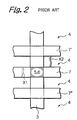
- Figs. 1A through 1F since the abrasive grain size is relatively large, flaws or scratches X as indicated in Figs. 1E and 1F are inevitably generated on the surface of the insulating layer 4. These flaws or scratches would short-circuit or disconnect upper wiring layers. That is, as illustrated in Fig. 2, which is a plan view of Fig. 1F, the conductive layer 7 (upper wiring layer) as well as its adjacent conductive layers 7' and 7" crosses over the conductive layer 3 (lower wiring layer).
- the conductive layer 7 is electrically connected via a plug formed by the barrier metal layer 5 and the metal layer 6 to the conductive layer 3, while there is no electrical connection between the conductive layers 7' and 7" and the conductive layer 3. Therefore, if a flaw or scratch as indicated by X1 in Fig. 2 is generated, the conductive layer 7 would be disconnected. Also, if a flaw or scratch as indicated by X2 in Fig. 2 is generated and metal is buried in the flaw or scratch, the conductive layers 7 and 7' would be short-circuited. This would reduce the manufacturing yield.
- the erosion effect is remarkably exhibited, which would fluctuate the parasitic capacitance of the wiring layers. That is, in the "metal CMP" process, in order to completely remove the barrier metal layer 5 and the metal layer 6 on the insulating layer 4, the barrier metal layer 5 and the metal layer 6 are overpolished. However, in this case, as illustrated in Fig. 3, the polishing rate of the barrier metal layer 5 and the metal layer 6 is larger in a tight pattern area PA1 than in a coarse pattern area PA2 since the stopping effect of the insulating layer 4 is larger in the coarse pattern area PA2 than in the tight pattern area PA2. As a result, the thickness of the insulating layer 4 fluctuates within the device, so that the parasitive capacitance of the insulating layer 4 fluctuates within the device, which would deteriorate the reliability.
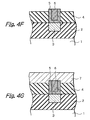
- an insulating layer 2 made of silicon oxide is deposited on a semiconductor substrate 1 by a CVD process. Then, a groove GV is perforated in the insulating layer 2 by a photolithography and dry etching process. Then, a conductive layer 3 made of W, Al or Cu is buried in the groove .GV of the insulating layer 2. In this case, the conductive layer 3 serves as a lower wiring layer.
- an about 500 nm thick insulating layer 4 made of silicon oxide is deposited on the entire surface by a CVD process.
- an about 50 nm thick sacrifice layer 11 made of silicon nitride (Si 3 N 4 ) is deposited on the insulating layer 4 by a CVD process.
- an about 500 nm diameter plug hole PH is perforated in the sacrifice layer 11 and the insulating layer 4 by a photolithography and dry etching process.
- an about 30 nm thick barrier metal layer 5 made of Ti or TiN and an about 600 nm thick metal layer 6 made of W, Al, Cu, or a multilayer or an alloy of two or more metals are sequentially deposited on the entire surface by a sputtering process.
- the metal layer 6 and the barrier layer 5 are flattened by a "metal CMP" process using the sacrifice layer 11 as a stopper.
- the sacrifice layer 11 is removed by a wet etching process using a phosphoric acid solution.
- an insulating layer made of silicon oxide (not shown) is deposited on the entire surface by a CVD process, and a groove (not shown) is perforated in the insulating layer by a photolithography and dry etching process. Then, a conductive layer 7 made of W or the like is buried in the groove.
- the conductive layer 7 serves as an upper wiring layer.
- the erosion effect is hardly exhibited, which would not cause the parasitic capacitance of the wiring layers to fluctuate. That is, in the "metal CMP" process, in order to completely remove the barrier metal layer 5 and the metal layer 6 on the insulating layer 4, the barrier metal layer 5 and the metal layer 6 are overpolished. Therefore, in this case, as illustrated in Fig. 6A, the polishing rate of the barrier metal layer 5 and the metal layer 6 is larger in a tight pattern area PA1 than in a coarse pattern area PA2 since the stopping effect of the sacrifice layer 11 is larger in the coarse pattern area PA2 than in the tight pattern area PA2. As a result, the thickness of the sacrifice layer 11 fluctuates within the device.
- the thickness of the insulating layer 4 remains uniform, so that the parasitive capacitance of the insulating layer 4 hardly fluctuates within the device.
- the device is not structurally affected, which would not deteriorate the reliability.
- the sacrifice layer 11 made of Si 3 N 4 can be etched by an anisotropic dry etching process using a mixture gas of CHF 3 and O 2 .
- the sacrifice layer 11 can be made of silicon oxide nitride (SiON), polycrystalline silicon, Al, Ti or TiN. If SiON is used, it may be etched by a wet etching process using a mixture solution of sulfuric acid and hydrogen peroxide or an anisotropic dry etching process using a mixture gas of CHF 3 /O 2 . If polycrystalline silicon is used, it may be etched by a wet etching process using a mixture solution of fluoric acid and acetic acid or a dry etching process using a gas of HBr.
- SiON silicon oxide nitride
- polycrystalline silicon it may be etched by a wet etching process using a mixture solution of fluoric acid and acetic acid or a dry etching process using a gas of HBr.
- Al it may be etched by a wet etching process using a mixture solution of nitric acid, acetic acid and phosphoric acid or a dry etching process using a gas of chlorine (Cl 2 ).
- Ti or TiN it may be etched by a wet etching process using a mixture solution of sulfuric acid and hydrogen peroxide with a mixing ratio of 4 ⁇ 5 to 1.
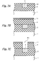
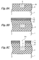
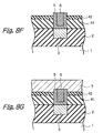
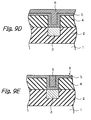
- Figs. 7A through 7I which illustrate a modification of the first embodiment
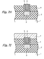
- Figs. 7A, 7B, 7C, 7D, 7E, 7H and 7I correspond to Figs. 4A, 4B, 4C, 4D, 4E, 4F and 4G, respectively, and the steps of Figs. 7F and 7G are added to the steps of the first embodiment. That is, after the "metal CMP" process is carried out at the step of Fig. 7E corresponding to Fig. 4E, the manufacturing process proceeds to a step as illustrated in Fig. 7F.
- a protection layer 12 made of photoresist is formed only on the plug formed by the barrier metal layer 5 and the metal layer 6 by a photolithography process.
- the sacrifice layer 11 is removed by a wet etching process or an anisotropic dry etching process as in the first embodiment.
- the protection layer 12 is removed to obtain the device as illustrated in Fig. 7H.
- an insulating layer 2 made of silicon oxide is deposited on a semiconductor substrate 1 by a CVD process. Then, a groove GV is perforated in the insulating layer 2 by a photolithography and dry etching process. Then, a conductive layer 3 made of W, Al or Cu is buried in the groove GV of the insulating layer 2. In this case, the conductive layer 3 serves as a lower wiring layer.
- an about 300 nm thick insulating layer 41 made of silicon oxide and an about 200 nm thick insulating layer 42 made of normal silicated glass (NSG) are deposited on the entire surface by a CVD process.
- an about 50 nm thick sacrifice layer 11 made of boron phospho-silicated glass (BPSG) is deposited on the insulating layer 42 by a CVD process.
- an about 500 nm diameter plug hole PH is perforated in the sacrifice layer 11 and the insulating layers 41 and 42 by a photolithography and dry etching process.
- an about 30 nm thick barrier metal layer 5 made of Ti or TiN and an about 600 nm thick metal layer 6 made of W, Al, Cu, or a multilayer or an alloy of two or more metals are sequentially deposited on the entire surface by a sputtering process.
- the metal layer 6 and the barrier layer 5 are flattened by a "metal CMP" process using the sacrifice layer 11 as a stopper.
- the sacrifice layer 11 is removed by a wet etching process using a mixture solution of fluoric acid and ammonium fluoride. In this wet etching process, the etching selectivity of the sacrifice layer 11 is enhanced.
- an insulating layer made of silicon oxide (not shown) is deposited on the entire surface by a CVD process, and a groove (not shown) is perforated in the insulating layer by a photolithography and dry etching process. Then, a conductive layer 7 made of W or the like is buried in the groove.
- the conductive layer 7 serves as an upper wiring layer.
- the erosion effect is hardly exhibited, which would not cause the parasitic capacitance of the wiring layers.
- the device is not structurally affected, which would not deteriorate the reliability.
- an insulating layer 2 made of silicon oxide is deposited on a semiconductor substrate 1 by a CVD process. Then, a groove GV is perforated in the insulating layer 2 by a photolithography and dry etching process. Then, a conductive layer 3 made of W, Al or Cu is buried in the groove GV of the insulating layer 2. In this case, the conductive layer 3 serves as a lower wiring layer.
- insulating layer 4 made of silicon oxide is deposited on the entire surface by a CVD process.
- an about 50 nm thick sacrifice layer 11 made of silicon nitride (Si 3 N 4 ) is deposited on the insulating layer 4 by a CVD process.
- an about 500 nm diameter plug hole PH is perforated in the insulating layer 4 by a photolithography and dry etching process.
- an about 30 nm thick barrier metal layer 5 made of Ti or TiN and an about 600 nm thick metal layer 6 made of W, Al, Cu, or a multilayer or an alloy of two or more metals are sequentially deposited on the entire surface by a sputtering process.
- the metal layer 6 is flattened by a "metal CMP" process, to expose the barrier metal layer 5.
- the barrier metal layer 5 is removed by a wet etching process using a mixture solution of sulfuric acid and hydrogen peroxide with a mixing ratio of 4 ⁇ 5 to 1 or a dry etching process using Cl 2 gas.
- an insulating layer made of silicon oxide (not shown) is deposited on the entire surface by a CVD process, and a groove (not shown) is perforated in the insulating layer by a photolithography and dry etching process. Then, a conductive layer 7 made of W or the like is buried in the groove.
- the conductive layer 7 serves as an upper wiring layer.
- the erosion effect is hardly exhibited, which would not cause the parasitic capacitance of the wiring layers to fluctuate.
- the device is not structurally affected, which would not deteriorate the reliability.
- the former may alternatively be located above the latter or vice versa.
- the conductive layer 3 and the plug formed by the barrier metal layer 5 and the metal layer 6 have the same width, the width of the conductive layer 3 may be smaller than that of the plug or vice versa.
- the barrier metal layer 5 and the metal layer 6 may form an upper wiring layer where the plug hole PH serves as a groove for the upper wiring layer.
- the conductive layer 3 serves as a plug between the upper wiring layer (5, 6) and a lower wiring layer 21 which may be made of an impurity diffusion region formed within the silicon substrate 1, or a conductive layer formed on the silicon substrate 1.
- the flaws or scratches that may be formed on the surface of the device as a result of a "metal CMP" process can be totally eliminated, the short-circuit or disconnection of the wiring layers can be avoided, which would enhance the manufacturing yield. Also, since the erosion effect due to the "metal CMP" process is hardly exhibited, the reliability of the device is not deteriorated.
Landscapes
- Internal Circuitry In Semiconductor Integrated Circuit Devices (AREA)
- Mechanical Treatment Of Semiconductor (AREA)
- Weting (AREA)
Abstract
Description
Claims (28)
- A method for manufacturing a semiconductor device, comprising the steps of:forming a first conductive layer (3) above a semiconductor substrate (1);forming a first insulating layer (4) on said first conductive layer;forming a sacrifice layer (11) on said first insulating layer;perforating a hole (PH) in said sacrifice layer and said first insulating layer;forming a second conductive layer (5, 6) on said sacrifice layer and within said hole;performing a metal chemical mechanical polishing operation upon said second conductive layer to expose said sacrifice layer; andremoving said sacrifice layer after said metal chemical mechanical polishing operation is performed.
- The method as set forth in claim 1, wherein said sacrifice layer is made of silicon nitride,
said sacrifice layer removing step carrying out a wet etching process using phosphoric acid solution. - The method as set forth in claim 1, wherein said sacrifice layer is made of silicon nitride,
said sacrifice layer removing step carrying out an anisotropic dry etching process using a mixture gas of CHF3 and O2. - The method as set forth in claim 1, wherein said sacrifice layer is made of silicon oxide nitride,
said sacrifice layer removing step carrying out a wet etching process using a mixture solution of sulfuric acid and hydrogen peroxide. - The method as set forth in claim 1, wherein said sacrifice layer is made of silicon oxide nitride,
said sacrifice layer removing step carrying out an anisotropic dry etching process using a mixture gas of CHF3 and O2. - The method as set forth in claim 1, wherein said sacrifice layer is made of polycrystalline silicon,
said sacrifice layer removing step carrying out a wet etching process using a mixture solution of fluoric acid and acetic acid. - The method as set forth in claim 1, wherein said sacrifice layer is made of polycrystalline silicon,
said sacrifice layer removing step carrying out a dry etching process using a gas of HBr. - The method as set forth in claim 1, wherein said sacrifice layer is made of aluminum,
said sacrifice layer removing step carrying out a wet etching process using a mixture solution of nitric acid, acetic acid and phosphoric acid. - The method as set forth in claim 1, wherein said sacrifice layer is made of aluminum,
said sacrifice layer removing step carrying out a dry etching process using a gas of chlorine. - The method as set forth in claim 1, wherein said sacrifice layer is made of titanium,
said sacrifice layer removing step carrying out a wet etching process using a mixture solution of sulfuric acid and hydrogen peroxide. - The method as set forth in claim 1, wherein said sacrifice layer is made of titanium nitride,
said sacrifice layer removing step carrying out a wet etching process using a mixture solution of sulfuric acid and hydrogen peroxide. - The method as set forth in claim 1, further comprising the steps of:forming a second insulating layer (2) on said semiconductor substrate; andperforating a groove (GV) in said second insulating layer,said first conductive layer forming step burying said first conductive layer in said groove.
- The method as set forth in claim 1, wherein said hole is a plug hole,
said second conductive layer forming a plug. - The method as set forth in claim 13, further comprising a step of forming a third conductive layer (7) on said plug after said sacrifice layer is removed.
- The method as set forth in claim 1, wherein said hole is a groove, said first conductive layer serving as a plug, said second conductive layer serving as a wiring layer.
- The method as set forth in claim 1, further comprising a step of forming a protection layer (5) only on said second conductive layer after said metal chemical mechanical polishing operation is performed and before said sacrifice layer is removed.
- The method as set forth in claim 16, wherein said protection layer is made of photoresist.
- The method as set forth in claim 1, wherein said first insulating layer forming step comprises the steps of:forming a silicon oxide layer (41) on said first conductive layer; andforming a normal silicated glass layer (42) on said silicon oxide layer.
- The method as set forth in claim 18, wherein said sacrifice layer is made of boron silicated glass,
said sacrifice layer removing step carrying out a wet etching process using a mixture solution of fluoric acid and ammonium fluoride. - The method as set forth in claim 1, wherein said second conductive layer is a stacked layer of barrier metal and metal, said barrier metal being made of one of titanium and titanium nitride, said metal being made of one of tungsten, aluminum and copper.
- A method for manufacturing a semiconductor device, comprising the steps of:forming a first conductive layer (3) above a semiconductor substrate (1);forming a first insulating layer (4) on said first conductive layer;perforating a hole (PH) in said first insulating layer;forming a barrier metal layer (5) on said first insulating layer and within said hole;forming a metal layer (6) on said barrier metal layer;performing a metal chemical mechanical polishing operation upon said metal layer to expose said barrier metal layer; andremoving an exposed portion of said barrier metal layer after said metal chemical mechanical polishing operation is performed.
- The method as set forth in claim 21, further comprising the steps of:forming a second insulating layer (2) on said semiconductor substrate; andperforating a groove (GV) in said second insulating layer,said first conductive layer forming step burying said first conductive layer in said groove.
- The method as set forth in claim 21, wherein said hole is a plug hole,
said second conductive layer forming a plug. - The method as set forth in claim 23, further comprising a step of forming a second conductive layer (7) on said plug after the exposed portion of said barrier metal layer is removed.
- The method as set forth in claim 21, wherein said hole is a groove, said first conductive layer serving as a plug, said barrier metal layer and said metal layer serving as a wiring layer.
- The method as set forth in claim 21, wherein said barrier metal is made of one of titanium and titanium nitride, said metal being made of one of tungsten, aluminum and copper.
- The method as set forth in claim 26, wherein said barrier metal layer removing step carrios out a wet etching process using a mixture solution of sulfuric acid and hydrogen peroxide.
- The method as set forth in claim 26, wherein said barrier metal layer removing step carries out a dry etching process using chlorine gas.
Applications Claiming Priority (2)
| Application Number | Priority Date | Filing Date | Title |
|---|---|---|---|
| JP11057947A JP2000260768A (en) | 1999-03-05 | 1999-03-05 | Method for manufacturing semiconductor device |
| JP5794799 | 1999-03-05 |
Publications (2)
| Publication Number | Publication Date |
|---|---|
| EP1039530A2 true EP1039530A2 (en) | 2000-09-27 |
| EP1039530A3 EP1039530A3 (en) | 2000-10-25 |
Family
ID=13070241
Family Applications (1)
| Application Number | Title | Priority Date | Filing Date |
|---|---|---|---|
| EP00104654A Withdrawn EP1039530A3 (en) | 1999-03-05 | 2000-03-03 | Method for manufacturing semiconductor device capable of avoiding flaws and erosion caused by metal chemical-mechanical polishing process |
Country Status (6)
| Country | Link |
|---|---|
| EP (1) | EP1039530A3 (en) |
| JP (1) | JP2000260768A (en) |
| KR (1) | KR100330024B1 (en) |
| CN (1) | CN1266278A (en) |
| CA (1) | CA2299813A1 (en) |
| TW (1) | TW463266B (en) |
Cited By (3)
| Publication number | Priority date | Publication date | Assignee | Title |
|---|---|---|---|---|
| US11232943B2 (en) * | 2019-04-24 | 2022-01-25 | Taiwan Semiconductor Manufacturing Co., Ltd. | Method and structure for semiconductor interconnect |
| CN114156178A (en) * | 2020-09-04 | 2022-03-08 | 中芯集成电路(宁波)有限公司 | Method for forming semiconductor structure |
| US11967568B2 (en) | 2021-09-17 | 2024-04-23 | Kabushiki Kaisha Toshiba | Semiconductor device |
Families Citing this family (15)
| Publication number | Priority date | Publication date | Assignee | Title |
|---|---|---|---|---|
| JP2003077917A (en) * | 2001-09-04 | 2003-03-14 | Sony Corp | Wiring formation method |
| US7291556B2 (en) | 2003-12-12 | 2007-11-06 | Samsung Electronics Co., Ltd. | Method for forming small features in microelectronic devices using sacrificial layers |
| KR100595141B1 (en) | 2004-12-31 | 2006-06-30 | 동부일렉트로닉스 주식회사 | Manufacturing method of semiconductor device to remove surface scratches caused by chemical mechanical polishing process |
| KR100840475B1 (en) | 2006-12-05 | 2008-06-20 | 동부일렉트로닉스 주식회사 | Metal wiring formation method of semiconductor device |
| JP4876231B2 (en) * | 2008-04-11 | 2012-02-15 | スパンション エルエルシー | Manufacturing method of semiconductor device |
| JP2012015540A (en) * | 2011-09-01 | 2012-01-19 | Spansion Llc | Semiconductor device |
| WO2013045973A1 (en) * | 2011-09-27 | 2013-04-04 | Chipworks, Incorporated | A method to differential p-channel or n-channel devices based on different etching rates. |
| JP5942867B2 (en) * | 2013-01-22 | 2016-06-29 | 富士通株式会社 | Manufacturing method of semiconductor device |
| CN103227146A (en) * | 2013-04-08 | 2013-07-31 | 上海华力微电子有限公司 | Method for fabricating tungsten through holes |
| JP5755314B2 (en) * | 2013-11-13 | 2015-07-29 | スパンション エルエルシー | Semiconductor device and manufacturing method of semiconductor device |
| KR101834418B1 (en) * | 2015-10-02 | 2018-03-05 | 유비머트리얼즈주식회사 | Slurry and substrate polishing method using the same |
| CN107978519A (en) * | 2017-11-16 | 2018-05-01 | 长江存储科技有限责任公司 | The manufacture method of tungsten grid in three dimensional NAND |
| CN111863712B (en) * | 2019-04-24 | 2024-07-16 | 台湾积体电路制造股份有限公司 | Semiconductor structure and method of forming a semiconductor structure |
| CN112864310B (en) * | 2019-11-26 | 2023-09-12 | 中芯国际集成电路制造(上海)有限公司 | Semiconductor structure and forming method thereof |
| CN115000008B (en) * | 2022-06-21 | 2025-07-18 | 上海华力集成电路制造有限公司 | Method for improving over etching of contact hole |
Family Cites Families (8)
| Publication number | Priority date | Publication date | Assignee | Title |
|---|---|---|---|---|
| JPS63128648A (en) * | 1986-11-18 | 1988-06-01 | Seiko Epson Corp | Semiconductor device |
| JP3005230B2 (en) * | 1989-06-10 | 2000-01-31 | ソニー株式会社 | Dry etching method for titanium-based materials |
| US5225034A (en) * | 1992-06-04 | 1993-07-06 | Micron Technology, Inc. | Method of chemical mechanical polishing predominantly copper containing metal layers in semiconductor processing |
| US5371047A (en) * | 1992-10-30 | 1994-12-06 | International Business Machines Corporation | Chip interconnection having a breathable etch stop layer |
| US5614765A (en) * | 1995-06-07 | 1997-03-25 | Advanced Micro Devices, Inc. | Self aligned via dual damascene |
| US5777370A (en) * | 1996-06-12 | 1998-07-07 | Advanced Micro Devices, Inc. | Trench isolation of field effect transistors |
| US5776833A (en) * | 1996-09-04 | 1998-07-07 | Mosel Vitelic Inc. | Method for forming metal plug |
| US5854140A (en) * | 1996-12-13 | 1998-12-29 | Siemens Aktiengesellschaft | Method of making an aluminum contact |
-
1999
- 1999-03-05 JP JP11057947A patent/JP2000260768A/en active Pending
-
2000
- 2000-03-01 CN CN00103033A patent/CN1266278A/en active Pending
- 2000-03-01 CA CA002299813A patent/CA2299813A1/en not_active Abandoned
- 2000-03-01 TW TW089103734A patent/TW463266B/en not_active IP Right Cessation
- 2000-03-02 KR KR1020000010489A patent/KR100330024B1/en not_active Expired - Fee Related
- 2000-03-03 EP EP00104654A patent/EP1039530A3/en not_active Withdrawn
Cited By (5)
| Publication number | Priority date | Publication date | Assignee | Title |
|---|---|---|---|---|
| US11232943B2 (en) * | 2019-04-24 | 2022-01-25 | Taiwan Semiconductor Manufacturing Co., Ltd. | Method and structure for semiconductor interconnect |
| US11961731B2 (en) | 2019-04-24 | 2024-04-16 | Taiwan Semiconductor Manufacturing Co., Ltd. | Method and structure for semiconductor interconnect |
| DE102020101284B4 (en) * | 2019-04-24 | 2025-04-30 | Taiwan Semiconductor Manufacturing Co., Ltd. | METHOD FOR SEMICONDUCTOR INTERCONNECT STRUCTURE |
| CN114156178A (en) * | 2020-09-04 | 2022-03-08 | 中芯集成电路(宁波)有限公司 | Method for forming semiconductor structure |
| US11967568B2 (en) | 2021-09-17 | 2024-04-23 | Kabushiki Kaisha Toshiba | Semiconductor device |
Also Published As
| Publication number | Publication date |
|---|---|
| KR100330024B1 (en) | 2002-03-27 |
| KR20000071404A (en) | 2000-11-25 |
| CN1266278A (en) | 2000-09-13 |
| TW463266B (en) | 2001-11-11 |
| EP1039530A3 (en) | 2000-10-25 |
| JP2000260768A (en) | 2000-09-22 |
| CA2299813A1 (en) | 2000-09-05 |
Similar Documents
| Publication | Publication Date | Title |
|---|---|---|
| EP1102315B1 (en) | A method to avoid copper contamination on the sidewall of a via or a dual damascene structure | |
| JP5220398B2 (en) | Electronic structure manufacturing method | |
| US5516346A (en) | Slurries for chemical mechanical polishing | |
| CA2299813A1 (en) | Method for manufacturing semiconductor device capable of avoiding flaws and erosion caused by metal cmp process | |
| US20020061635A1 (en) | Solution for chemical mechanical polishing and method of manufacturing copper metal interconnection layer using the same | |
| US5854140A (en) | Method of making an aluminum contact | |
| WO1999063591A1 (en) | Dual-damascene interconnect structures employing low-k dielectric materials | |
| US7166532B2 (en) | Method for forming a contact using a dual damascene process in semiconductor fabrication | |
| US6218283B1 (en) | Method of fabricating a multi-layered wiring system of a semiconductor device | |
| US5776833A (en) | Method for forming metal plug | |
| JP2003179136A (en) | Mask layer and interconnect structure for dual damascene semiconductor fabrication | |
| JPH09283522A (en) | Method of forming metal wiring | |
| KR100350111B1 (en) | Wiring of Semiconductor Device and Method for Manufacturing Thereof | |
| US6251789B1 (en) | Selective slurries for the formation of conductive structures | |
| US6919276B2 (en) | Method to reduce dishing and erosion in a CMP process | |
| US6723626B2 (en) | Method of manufacturing semiconductor device | |
| US6746954B2 (en) | Method of reworking tungsten particle contaminated semiconductor wafers | |
| US6413869B1 (en) | Dielectric protected chemical-mechanical polishing in integrated circuit interconnects | |
| US20020048934A1 (en) | Planarization method on a damascene structure | |
| US20020053738A1 (en) | Semiconductor device with improved metal interconnection and method for forming the metal interconnection | |
| US20030003712A1 (en) | Methods for fabricating a semiconductor device | |
| US6468897B1 (en) | Method of forming damascene structure | |
| US6699785B2 (en) | Conductor abrasiveless chemical-mechanical polishing in integrated circuit interconnects | |
| US20020173140A1 (en) | Conductor chemical-mechanical polishing in integrated circuit interconnects | |
| US7381638B1 (en) | Fabrication technique using sputter etch and vacuum transfer |
Legal Events
| Date | Code | Title | Description |
|---|---|---|---|
| PUAI | Public reference made under article 153(3) epc to a published international application that has entered the european phase |
Free format text: ORIGINAL CODE: 0009012 |
|
| PUAL | Search report despatched |
Free format text: ORIGINAL CODE: 0009013 |
|
| AK | Designated contracting states |
Kind code of ref document: A2 Designated state(s): DE FR GB IT NL |
|
| AX | Request for extension of the european patent |
Free format text: AL;LT;LV;MK;RO;SI |
|
| AK | Designated contracting states |
Kind code of ref document: A3 Designated state(s): AT BE CH CY DE DK ES FI FR GB GR IE IT LI LU MC NL PT SE |
|
| AX | Request for extension of the european patent |
Free format text: AL;LT;LV;MK;RO;SI |
|
| 17P | Request for examination filed |
Effective date: 20001004 |
|
| AKX | Designation fees paid |
Free format text: DE FR GB IT NL |
|
| STAA | Information on the status of an ep patent application or granted ep patent |
Free format text: STATUS: THE APPLICATION HAS BEEN WITHDRAWN |
|
| 18W | Application withdrawn |
Withdrawal date: 20020227 |