BACKGROUND OF THE INVENTION
Field of the Invention
The present invention relates to an optical
communication system, in particular, to an optical network
with fault recovery capabilities.
Discussion of the Background
The explosive growth of the Internet, which has millions
of users, has and will continue to generate enormous data
traffic over the backbone networks of the Internet. These
backbone networks correspondingly require greater bandwidth
in the transmission paths to support the many user
applications, from email to streaming video. By the same
token, any disruption along the transmission paths of the
backbone networks would adversely affect countless numbers of
users. Such a disruption may stem from a cable cut, or some
other fault (e.g., equipment failure).
The effects of the disruption range from increased
response times to data loss. When the traffic is mission
critical, any loss of information is unacceptable. Hence,
along with greater bandwidth demand from the users, service
providers are required to guarantee extremely high network
reliability, which in turn requires spare capacity.
It has been recognized that fiber optic cables hold the
promise of being able to rapidly transport vast amounts of
traffic. Thus, development in optical communications
networks has steadily progressed. SONET (synchronous optical
network), which is promulgated by the American National
Standards Institute (ANSI), has emerged as an accepted
standard defining the transport and management of data
traffic over fiber optic transmission systems. An important
feature of SONET is its ability to automatically recover from
network faults.
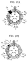
A conventional SONET ring network, as schematically
shown in FIG. 16, utilizes four optical fibers to transport
data, in which two optical fibers 1a and 1b are designated as
working, while the other two 2a and 2b are considered
protection fibers. The fibers 1 and 2 connect five SONET
nodes, N1-N5. The optical signals within the working fiber
pairs 1a and 1b are normally transmitted in opposite
directions, as indicated by the arrowheads. Similarly,
within the protection fiber pairs 2a and 2b, the fiber line
2a carry optical signals in an opposite direction to the
optical signals that are transmitted by fiber line 2b. As
will be discussed more fully below, the optical signals that
are transmitted via the working fiber pairs 1 are switched
over to the protection pairs 2a and 2b upon occurrence of a
fault; SONET nodes N1 - N5 are SONET add/drop equipment for
adding and dropping the optical signals to and from the
working optical fibers 1a and 1b. and the protection optical
fibers 2a and 2b.
The add/drop function within SONET is performed at the
electrical level; accordingly, a SONET node must temporarily
convert the optical signals into electrical signals before
processing the optical signals. Based upon examination of
the electrical signals, the SONET node can determine whether
a fault has occurred in the network.
FIG. 16 shows an operational scenario in which all the
transmission paths 1a, 1b, 2a, and 2b as well as the nodes
N1-N5 are fully functioning. In this example, when an
optical signal is added to the node N3 (as indicated by the
arrowhead A) and is destined to node N1. The optical signal
follows the shortest route, and thus, is transmitted in a
clockwise direction via optical fiber 1b to the destination
node N1. The optical signal is then dropped at node N1, as
indicated by the arrowhead D. On the other hand, if an
optical signal is added to node N1, as indicated by the
arrowhead A, the optical signal is transmitted
counterclockwise via optical fiber 1a to the destination node
N3 (which is the shortest route). Next, the transmitted
optical signal is dropped at node N3.
Although not illustrated in FIG. 16, a node connected to
another ring network is provided with cross-connect
functionality to switch the optical signals over to the other
network. That is, under the conventional approach, to link
one optical communications network to another, an electrical
cross-connect converts the optical signals into electrical
signals, then reconverting some of the electrical signals, if
necessary, into optical signals for transmission over the
other ring network.
FIGs. 17A and 17B illustrate the operation of the SONET
ring, whereby the optical fibers between nodes N1 and N2 are
totally and partially down, respectively. The protection
function of the SONET layer works to set alternative
transmission paths in the ring network. Under these fault
conditions, alternative routing of the optical signals can be
achieved using two protection schemes: (1) ring protection,
and (2) span protection. The architecture of the SONET ring
in FIGs. 17A and 17B resembles that of FIG. 16, in which five
nodes are interconnected via four optical fibers (i.e., an
working pair 1 and a protection pair 2).
FIG. 17A shows an alternative routing scheme known as
"ring protection", in which all four optical fibers (i.e.,
working optical fibers 1a and 1b and protection optical
fibers 2a and 2b) simultaneously fail. Under this scenario,
a fault Os occurs between the node N1 and the node N2 in the
ring network. The ring protection system sets an alternative
route by detecting faults in the fiber links, in this case,
between the nodes N1 and N2. Based upon detection of fault
Os, the ring protection system connects the working optical
fiber 1a to the protection optical fiber 2b, and the working
optical fiber 1b to the protection optical fiber 2a.
According to the ring protection scheme, the optical signal
added in the node N3, as indicated by the arrowhead A, is
carried by the working optical fiber 1b. The shortest route
to the destination node N1 is in the clockwise direction via
node N2. Upon the optical signals reaching node N2, node N2
recognizes that both the working pairs 1 and the protection
pairs 2 are disconnected due to some fault. Accordingly,
node N2 switches the optical signal over to the protection
optical fiber 2a. The optical signal, thereafter, is
transmitted in the counterclockwise direction to the node N1,
where the optical signal is dropped (as indicated by the
arrowhead D) from the protection optical fiber 2a.
In a converse situation, node N1 adds an optical signal
to the protection optical fiber 2b. After the optical signal
is transmitted clockwise, it temporarily passes through the
destination node N3 so that node N2 may switch the optical
signal over to the working optical fiber 1a. Node N2
transmits the optical signal in a counterclockwise direction
and drops the optical signal from the working optical fiber
1a at destination node N3, as indicated by the arrowhead D.
FIG. 17B shows the operation of an alternative routing
scheme known as "span protection". As shown, a fault Os
occurs between the node N1 and the node N2 in the ring
network, in which the working optical fibers 1a and 1b
experience failure. Under this scenario, the span protection
system detects a fault between nodes N1 and N2, involving
both working optical fibers 1a and 1b. After detection of
this fault Os, the span protection system utilizes protection
optical fibers 2a and 2b in that particular span where
working lines 1a and 1b failed.
In the example of FIG. 17B, node N3 adds an optical
signal to the working optical fiber 1b, and transmits the
optical signal clockwise to node N2. Node N2 then switches
the optical signal over to protection optical fiber 2b,
transmitting the optical signal in a clockwise direction, and
dropping it in the destination node N1.
In the case where an optical signal is added at node N1
to the protection optical fiber 2a, node N1 transmits the
optical signal in a counterclockwise direction to node N2.
Node N2 switches the optical signal over to the working
optical fiber 1a, and transmits the optical signal
counterclockwise, dropping the optical signal at node N3.
Although SONET does provide the necessary fault recovery
mechanisms, it has some limitations with respect to bandwidth.
Because SONET is based on a time division multiplexing (TDM)
scheme, the achievable transmission rates are constrained by
physical characteristics of the fiber optic cables. In some
instances, to obtain more bandwidth, more fiber optic cables
need to be added to the install base, which in a number of
cases is a cost prohibitive proposition.
Therefore, service providers have turned to wavelength
division multiplexing (WDM) to meet the need for higher
bandwidths. WDM technology has emerged to address the
bandwidth demand by increasing the number of communication
channels in an optical network; notably dense wavelength
division multiplexing (DWDM) has opened a new door to very
high bandwidth. DWDM systems utilize different, closely-spaced
wavelengths to carry information.
The SONET ring network of FIG. 16 can be converted to a
WDM network by transmitting optical signals that are
wavelength-multiplexed signals; this requires that the
appropriate WDM optical add/drop equipment be used for nodes
N1-N5.
However, as evident from the above discussion, the SONET
add/drop function and associated protection function are
attained at the electrical level. That is, these functions
require that the optical signals be converted to electrical
signals for processing and then converted back to optical
signals for transport. This process of conversion and
reconversion is also characteristic of general WDM
communications systems. Furthermore, the WDM optical signals
not only increase the cost of SONET equipment, but increases
the complexity of the node function. Accordingly, this
process of converting from optical to electrical and vice
versa is inefficient.
It is therefore desirable to obtain SONET layer
protection functions at the optical level. To achieve this
objective, the optical add/drop function, and the optical
cross-connect function need to be carried out without optical
to electrical conversion.
One conventional approach to providing a protection
function in an optical layer is to deploy a waveguide type
4x4 matrix optical switch, which is made up of 16-pieces of
1x2 type and 2x2 type unit optical switches in an optical
network of FIG. 16. The unit optical switches in this
conventional matrix optical switch are provided as planar
waveguides on the same substrate. A drawback with the
waveguide type 4x4 matrix optical switch approach is the use
of a large number of the unit optical switches (i.e.,16). As
a consequence, the corresponding insertion loss can reach up
to 6.6 dB. Hence, this system requires an expensive optical
amplifier to compensate for the insertion loss of this 4x4
matrix optical switch. Additionally, the waveguide type 4x4
matrix optical switch provides a large number of connection
states between the I/O ports; e.g., the number of states can
be 24 (4x3 x 2x1 = 24). However, the protection function, as
described above, can be achieved with less than 24 connection
states. Accordingly, this arrangement provides a less than
efficient and more costly solution. Another drawback with
the waveguide type 4x4 matrix optical switch concerns
electrical power consumption. The matrix optical switch
requires a continuous voltage to all four optical switches in
order to keep the desired connection state between the I/O
ports.
In the optical line switching system described above,
when the protection function is invoked, the plurality of
unit optical switches are required to be simultaneously
switched. Hence, the probability of malfunction increases,
which negatively impacts reliability of the system.
Based on the foregoing, there is a clear need for
improved approaches for providing protection function in an
optical layer.
There is a need to minimize the cost of network
operation by reducing the number of optical switch units and
optical amplifiers.
There is also a need to minimize electrical power
consumption in an optical communications network.
There is further a need for improving network
reliability of an optical communications network.
Based on the need to supply reliable network services in
a high bandwidth environment, an approach for performing
fault recovery at the optical layer is highly desirable.
SUMMARY OF THE INVENTION
According to an aspect of the invention, an optical line
switching system comprises an optical switch connected to
working optical fibers and protection optical fibers. The
optical switch is configured to switch over optical signals
among the working optical fibers and the protection optical
fibers. The optical switch comprises a plurality of unit
optical switches and a common driving mechanism that is
configured to perform simultaneously switching operation of
the unit optical switches to alter the switching state of the
optical switch. A plurality of monitoring devices are
coupled to the working optical fibers and the protection
optical fibers and configured to monitor the optical signals
transmitted over the working optical fibers and the
protection optical fibers. The monitoring devices are
configured to output selectively monitoring signals that
indicate one or more faults in the working optical fibers and
the protection optical fibers. A control device is coupled
to the monitoring devices and configured to output a control
signal to the optical switches to effect an optical
protection scheme by selectively changing switching states of
the optical switches in response to the monitoring signals.
Under this approach, the number of optical switches is
minimized, while retaining the optical protection functions
of the ring and span protection schemes.
According to one aspect of the invention, a method of
providing an optical protection system that utilizes an
working transmission path and a protection transmission path
comprises transmitting optical signals over the working
transmission path and the protection transmission path. The
method includes performing an optical add/drop function and a
multiplex/demultiplex function on the optical signals and
monitoring the transmission of the optical signals over the
transmission paths. A monitoring signal is generated to
indicate whether a fault in the transmission paths has
occurred. Further, the method includes outputting control
signals to a plurality of optical switches to effect an
optical protection scheme in response to the monitoring
signal. The method also includes altering switching states
of the plurality of optical switches in response to the
control signal of the outputting step. Each of the plurality
of optical switches comprises unit optical switches that are
simultaneously operated by a common driving mechanism. The
above arrangement advantageously reduces power consumption.
In yet another aspect of the invention, an optical
communications network for providing fault recovery
capabilities, comprises a plurality of optical fibers and a
plurality of nodes that exchange optical signals over the
optical fibers. The plurality of nodes are arranged
according to a prescribed topology. Each of the nodes
comprises an optical switch that is connected to the optical
fibers and is configured to switch the optical signals among
the optical fibers. The optical switch includes a plurality
of unit optical switches and a common driving mechanism that
is configured to perform simultaneously switching operation
of the unit optical switches to alter the switching state of
the optical switch. The node also includes a plurality of
monitoring devices that are coupled to the optical fibers.
The monitoring devices are configured to monitor the optical
signals that are transmitted over the optical fibers and to
output selectively monitoring signals that indicate one or
more faults in the optical fibers. Further, each of the
nodes includes a control device that is coupled to the
monitoring devices and is configured to output a control
signal to the optical switches to effect an optical
protection scheme by selectively changing switching states of
the optical switch in response to the monitoring signals.
Under this arrangement, a high reliable optical
communications network is achieved, in part by decreasing the
probability of switch malfunction by effecting a protection
function using a minimal number of switch operations.
In yet another aspect of the invention, an optical
switching device comprises a first optical switch and a
second optical switch that is coupled with the first optical
switch to form a common switching fabric. Each of the
optical switches comprises two unit optical switches and a
common driving mechanism that is configured to simultaneously
operate the two unit optical switches. This arrangement
permits the use of a minimal number of optical switches that
are utilized in an optical communications network with fault
recovery capabilities.
Other features and advantages of the present invention
will become readily apparent from the following description
taken in conjunction with the accompanying drawings.
BRIEF DESCRIPTION OF THE DRAWINGS
A more complete appreciation of the invention and many
of the attendant advantages thereof will be readily obtained
as the same becomes better understood by reference to the
following detailed description when considered in connection
with the accompanying drawings, wherein:
DESCRIPTION OF THE PREFERRED EMBODIMENTS
In the following description, for the purpose of
explanation, specific details are set forth in order to
provide a thorough understanding of the invention. However,
it will be apparent that the invention may be practiced
without these specific details. In some instances, well-known
structures and devices are depicted in block diagram
form in order to avoid unnecessarily obscuring the invention.
The present invention accomplishes fault recovery in an
optical communications network, which utilizes working
transmission paths and protection transmission paths.
Additionally, the optical protection system, according to
some embodiments of the present invention, provides recovery
from internal component failures within a node of the optical
communications network. The node implements a ring
protection scheme and a span protection scheme at the optical
layer. According to one embodiment, an optical line
switching system (i.e., node) has optical switches connected
to optical signal processing devices (e.g., optical add/drop
multiplexers (OADMs), and optical cross-connects), in which
each of the optical switches is made up of two unit optical
switches, which share a common driving mechanism. This
common driving mechanism performs simultaneous switching
operation of the unit optical switches to change switching
states of the optical switches when an optical protection
scheme (e.g., the ring protection scheme or span protection
scheme) is invoked. To execute the protection scheme at the
optical layer, photo diodes are deployed to monitor the
transmission of optical signals over the transmission paths.
Further, the node includes a control device that outputs
control signals, as a result of a detected fault, to instruct
the optical switches to change states.
Although the present invention is discussed with respect
to mechanical optical switches that effect a ring protection
and span protection schemes, it should be appreciated that
one of ordinary skill in the art would recognize that the
present invention has applicability to other types of optical
switches and other protection schemes. Further, although the
various embodiments of the present invention describe the use
of dual switches, it is recognized that any interlocking
switch may be utilized.
Embodiments of an optical line switching system
according to the present invention will hereinafter be
described in detail with reference to FIGs. 1 through 15. In
particular, eight embodiments of the present invention are
discussed. However, as will become apparent, other
embodiments are possible.
Embodiment 1
Referring now to the drawings, wherein like reference
numerals designate identical or corresponding parts
throughout the several views, and more particularly to FIGs.
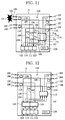
1A and 1B thereof, an optical line switching system 10 is
shown. The optical line switching system 10 constitutes a
node N of an optical communications network. As seen in FIG.
1A, the node N 10 includes optical signal processing devices
11 and 12 as well as optical switches 13 -18. The optical
signal processing devices 11 and 12 provide an add/drop
function and a multiplexing/demultiplexing function; in
addition, the optical signal processing devices 11 and 12 may
also have cross-connect functionality. The term, optical
signal processing device, as used herein, refers to an
optical add/drop multiplexer (OADM) and/or a cross-connect
equipment. Photo diodes 19 - 22 are utilized as monitoring
devices to detect line faults in either the working or
protection transmission path. An electronic control unit
(ECU) 24 controls the switching states of the optical
switches 13-18 to effect an optical protection scheme, such
as the ring protection scheme and the span protection scheme.
According to this exemplary embodiment, the optical
communications network follows a ring topology. The ring
network is a four fiber system, in which optical fibers 5 and
6 serve as working transmission paths and optical fibers 7
and 8 provide protection transmission paths. Under this
exemplary network topology, it is assumed that optical
signals are transmitted bidirectionally, both in a clockwise
direction (i.e., right to left) over fibers 6 and 7 as well
as in a counterclockwise direction (i.e., left to right) over
fibers 5 and 8. To maximize system bandwidth, protection
fibers 7 and 8 can be utilized to carry lower priority
traffic. Once a fault occurs, the optical signals that are
carried on the working fibers 5 and 6 are switched over to
the protection fibers 7 and 8. This will result in
disruption of service to those users who are transmitting
information over the protection fibers 7 and 8. However,
service involving data transmission over the protection
fibers 7 and 8 are ideal for users who are more concerned
with telecommunication costs than 100% network availability.
The internal connectivity of node N 10 is designed to
quickly and efficiently recover from transmission line faults.
As seen from FIG. 1A, the working fiber 5 enters node N 10
from a node N-1 (not shown) on the left side. A photo diode
19 receives optical signals via working fiber 5, which in
turn forwards the optical signals to an optical switch 13.
The optical signals from working fiber 5, thereafter, are
sent through an optical amplifier 26, an optical signal
processing device 11, another optical amplifier 28, and an
optical switch 14. The optical signals then exit node N 10
on the right side over working fiber 5 to another node N+1
(not shown).
The other working fiber 6 enters the node N 10 on the
right from node N+1 (not shown). The working fiber 6 carry
optical signals that, under normal operation, are transmitted
through the following sequence of components: a photo diode
20, an optical switch 17, an optical amplifier 27, an optical
signal processing device 12, another optical amplifier 29 and
an optical switch 16. Optical amplifiers 26, 27, which are
situated upstream of the optical signal processing devices 11
and 12, provide amplification of the optical signals before
these optical signals are processed by the optical signal
processing devices 11 and 12.
However, optical amplifiers 28, 29 are placed downstream
from the optical signal processing devices 11 and 12,
ensuring that sufficient optical power exists to transmit the
optical signals up to the adjacent node. The gains of the
optical amplifiers 26 - 29 can be set to offset any
anticipated signal attenuation.
The optical signal processing devices 11 and 12 are
provided in the working optical fibers 5 and 6 to perform an
optical add/drop function. In this manner, optical signals
can be added and dropped from a composite optical signal,
which may include, for example, 16 separate data streams that
are carried by different wavelengths. In contrast, a
conventional SONET system requires that the add/drop function
be performed at an electrical level, which necessitates the
conversion from electrical to optical signals; once the
electrical signals are processed, they are converted back to
the optical domain. In an exemplary embodiment, a fiber
Bragg grating (FBG) that provides an optical add/drop
function may be used as an optical signal processing device.
The optical signals that are carried over protection
fiber 7 enter node N 10 from node N+1(not shown) and are
received by photo diode 21. The photo diode 21 is connected
to optical switch 14. An optical amplifier 30 serves to
amplify the optical signals on the fiber between optical
switch 14 and optical switch 13 to compensate for
transmission loss (in the case of optical signals emanating
from node N+1) and to supply ample optical power for
transmitting the optical signal to another node (e.g., N-1).
Optical switch 13 transmits the optical signals out to node
N-1 (not shown).
As for optical signals that are transported by
protection fiber 8, these optical signals traverse through
node N 10 from node N-1 (not shown) on the left side,
according to the following sequence of components: a photo
diode 22, an optical switch 16, an optical amplifier 31, and
an optical switch 17. An optical amplifier 31 is provided
between optical switches 16 and 17 to compensate for a node-to-node
span loss between adjacent nodes. Likewise, an
optical amplifier 31 is provided between optical switches 16,
17. Each of the optical amplifiers 26 - 31 may be, for
example, an Erbium Doped Fiber Amplifier (EDFA). EDFAs are
passive amplifiers, and thus, exhibit high reliability.
Turning now to the architecture of the optical line
switching node, it is seen in FIG. 1A that each of the
optical switches 13-18 has four I/O ports, as indicated by
the circles. These optical switches 13-18 are interconnected
via their respective input and output ports, using a
multitude of fiber optic cables. Optical switch 15 is
coupled between switches 13 and 14; similarly, optical switch
18 is linked between optical switches 16 and 17. Further,
optical attenuators 34 - 37 are placed, respectively, on the
optical fibers that provide connections between optical
switches 13 and 15; between optical switches 14 and 15;
between optical switches 16 and 18; and between optical
switches 17 and 18. Each of the optical attenuators 34 and
35 has an attenuation quantity that is set to correspond to
the gain of optical amplifier 30. In addition, each of the
optical attenuators 36 and 37 has an attenuation quantity
corresponding to the gain of optical amplifier 31.
In a fault free situation as shown in FIG. 1A, all the
optical switches 13-18 are in a bar-state. According to one
embodiment of the present invention, a bar-state is one of
two possible switching states; the other switching state is a
cross-state. A switching state defines the mapping between
the input ports and the output ports of a particular optical
switch. It should be noted that "switching state" differs in
meaning from the term, connection state, as used earlier.
Connection state denotes the port mapping for the collective
optical switch; this is distinguished from a switching state,
which defines the port mapping for a particular unit optical
switch. In general terms, the bar-state is one particular
mapping, and the cross-state is another mapping. These
switching states are more fully defined in the discussion of
FIGs. 2A and 2B.
The optical switches 13-18 are configured with optical
layer protection functionalities, and as such, these optical
switches 13-18 are capable of determining which protection
system, the ring protection system or the span protection
system, is being effected.
The above node arrangement enhances network reliability
and reduces network cost by decreasing the number of system
components that are required to implement the optical network
protection schemes. Particularly, the number of optical
switches and optical amplifiers are minimized relative to the
conventional system. Further, the number of switch
operations is decreased, thereby correspondingly reducing the
likelihood of switch malfunction.
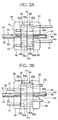
FIGs. 2A and 2B show a dual 2x2 optical switch in
accordance with an embodiment of the present invention. This
type of interlocking switch may be used as each of the
optical switches 13-18 within node N 10. The term
"interlocking type optical switch" is used herein to define a
composite switch that includes two or more unit switches
having a common driving mechanism. As illustrated in FIGs.
2A and 2B, the optical switch has a first ferrule 50, which
is fixed, and a second ferrule 60, which is movable in two
separate positions (i.e., shown in FIGs. 2A and 2B). A
refractive index matching oil (not shown) fills the gap
between the alignment side end surfaces of these ferrules.
As seen in FIG. 2A, the first ferrule 50 has four
strands of optical fibers 51-54 along with two loop- back
fibers 55 and 56. The first ferrule 50 also possesses two
sets of pin holes 50a and 50b formed in two side ends of each
of these fibers 51-56. The second ferrule 60 has four
strands of optical fibers 61-64 and loop- back fibers 65 and
66. Two sets of pin holes 60a and 60b, corresponding to the
two sets of pin holes 50a and 50b in the first ferrule, are
formed in two side ends of each of these fibers 61-66. The
other ends of the loop- back fibers 65 and 66 are spliced at
fusing points PFS to the other ends of the loop- back fibers
55 and 56.
As mentioned above, FIG. 2A shows a bar-state switching
state of a dual 2x2 optical switch, in accordance with an
embodiment of the present invention. In a bar-state, the two
ferrules 50 and 60 are positioned such that when pins 71 are
inserted into the corresponding pin holes 50a and 60a, the
optical fiber strands 51-54 align with optical fiber strands
61-64, respectively. Loop- back fibers 65 and 66 are not
aligned with any of the optical fiber strands 51-54.
To achieve a cross-state switching state (as shown in
FIG. 2B), the pins 71 are removed from pin hole 60a of the
second ferrule 60, and pin 72 is inserted into the pin holes
50b and 60b. The pins 71 and 72 have tapered tips for ease
of insertion upon forward movement into the corresponding
holes. In this configuration, the optical fibers 51-54 line
up at the alignment side end surfaces to the optical fibers
62, 61, 64, and 63, respectively. Unlike the bar-state, the
loop- back fibers 55, 56, 65, and 66 in the cross-state are
used to map optical fibers 52 and 54 to optical fibers 61 and
63, respectively. That is, in the optical fiber 52 to
optical fiber 61 mapping, a transmission path is formed by
the following sequence: optical fiber 52, loop-back fiber 65,
loop-back fiber 55, and optical fiber 61. The mapping of
optical fiber 54 to optical fiber 63 provides the following
sequence: optical fiber 54, loop-back fiber 66, loop-back
fiber 56, and optical fiber 63.
To manipulate the pins 71 and 72 in the manner described
above, a common driving element (not shown) is needed. One
exemplary mechanism, in accordance with an embodiment of the
present invention, is a solenoid coil, which moves the pins
71 and 72 forward and backward. These pins 71, 72 are fitted
to a common driving element so that the pins 71 and 72 are
driven together, whereby the forward movement of the pins 71
and the backward movement of the pins 72 are executed
simultaneously; likewise, the backward movement of the pin 71
and the forward movement of the pin 72 are executed
simultaneously. When a solenoid coil is utilized as the
common driving element, the solenoid coil requires electric
power to move the pins 71 and 72. One advantage of this type
of switching system is that no extra electric power is
required to retain the switching state. In other words, once
the pins 71 and 72 are in placed, their positions are
maintained until a change in switching state occurs without
any extra supply of voltage.
The alternative paths within node N 10 are created by
the various configuration of the multiple unit optical
switches that constitute an optical switch. The number of
operations of the optical switch when the protection function
is invoked can be reduced in half by controlling two unit
optical switches with a single common signal; for example, by
simultaneously applying a common voltage to both unit optical
switches. That is, a common driving element can be used to
perform simultaneously the switching operation of the unit
optical switches.
As mentioned above, the first and second ferrules 50 and
60 constitute two 2x2 type unit optical switches. The
optical fibers 51, 52, 61, and 62 form one set of I/O optical
fibers of the first 2x2 type unit optical switch. Another
2x2 type unit optical switch is constructed by use of the
optical fibers 53, 54, 63, and 64 as a second set of I/O
optical fibers. By using the interlocking type optical
switch of FIGs. 2A and 2B for the optical switches 13-18, two
switching operation patterns result, as shown in FIG. 3A.
One of ordinary skill in art would recognize that other
interlocking type switches, such as silica-based waveguide
type thermo-optic switches, can be readily utilized. Under
this implementation, an arrangement involving thermo-optic
phase shifter elements, which are composed of two pieces of
thin film heaters that are mounted respectively in the two
unit optical switches, are electrically wired in series.
As previously indicated, four switching states exist
with these interlocking type optical switches; According to
one embodiment, the 2-way switching operation patterns are
defined as independent switching operations. It should be
noted that the switching operation pattern in FIG. 3A is
never switched over to the switching operation pattern in FIG.
3B.
The optical switches 13-18 change their switching states,
depending on the conditions of the working and protection
fibers 5-8. Thus, a monitoring device is needed to track
whether a fault has occurred in the fibers 5-8. According to
one embodiment of the present invention, photo diodes 19-22
serve as the monitoring devices. These photo diodes 19-22
are attached to the working and protection fibers 5-8,
respectively, so that a fault in the line can be detected.
An electronic control unit 24 collects signal power
information from the photo diodes 19-22.
To monitor whether a fault has occurred on any of these
optical fibers 5-8, the photo diodes 19-22 receive input
optical signals into node N 10 from working optical fibers 5
and 6 and standby optical fibers 7 and 8. The photo diodes
19-22 are situated within the node N 10 so that they measure
the power levels of the optical signals entering the node N
10 (i.e., optical signals that are transmitted from nodes N-1
and N+1). These photo diodes 19-22 are connected to ECU 24;
the connections are not shown. Photo diodes 19-22 may also
output monitoring signals to an ECU that resides in an
adjacent node, depending on which optical fiber is being
monitored and where the optical fiber is located.
Based on the signals transmitted from the photo diodes
19-22, the electronic control unit 24 controls the switching
states of the optical switches 13-18 by outputting control
signals to one or more predetermined optical switches among
the optical switches 13-18. For example, if the power level
of the optical signals in any of the working optical fibers 5
and 6 or the protection optical fibers 7 and 8 falls below a
predetermined value, the ECU 24 generates control signals to
the appropriate optical switches to redirect the transmission
path in accordance with a ring protection scheme or a span
protection scheme to circumvent the failed links.
FIG. 1B shows the occurrence of line faults Os in the
working optical fibers 5, 6 and in the protection optical
fiber 7 in the node of FIG. 1A. In accordance with
Embodiment 1, the working and protection optical fibers 5 and
7, and the working and protection optical fibers 6 and 8 are
respectively independently paired. In other words, each of
the pairs of working and protection optical fibers 5/7 and
6/8 has the capability to independently perform the optical
protection scheme based upon the location of the fiber faults.
In this scenario, the electronic control unit 24, based on
the signals outputted from the photo diodes 19, 20 as well as
a photo diode of node N-1 (not shown), outputs control
signals to optical switches 13, 17, and 18 to change the
switching states from the bar-state to the cross-state.
Upon receiving the control signals, optical switches 13,
17, and 18 cooperatively to effect alternate transmission
paths (as indicated by the bold lines in FIG. 1B) to recover
from the faults Os. Because the faults Os affect both
working optical fiber 5 and protection optical fiber 7 on the
left side of the node N 10, optical signals that are carried
by protection optical fiber 7 travel to an optical amplifier
30. The optical amplifier 30, which is attached to the
protection optical fiber 7, compensates for signal loss
between the nodes (in this instance nodes N+1 and node N) and
relays the amplified optical signals to optical switch 13.
In this fault condition, the signal arriving at the right
side from node N+1 on fiber 7 is amplified by three
amplifiers 30, 26, and 28. The collective amplification by
these three amplifiers 30, 26, and 28 is too high.
Accordingly an attenuator 34 is needed to cancel the effect
of amplifier 30; this is also described below with respect to
FIG. 6B
As seen in FIG. 1B, optical switch 13 switches the
optical signals to optical switch 15. The optical signals
are looped back by optical switch 15 to a different port on
optical switch 13. The optical switch 13 then switches the
optical signals to the appropriate port that is connected to
optical signal processing device 11. Prior to reaching
optical signal processing device 11, the optical signals are
amplified by optical amplifier 26. After processing the
received optical signals, the optical signal processing
device 11 transmits the optical signals to optical amplifier
28 for amplification. Thereafter, the optical signals are
transmitted by the optical amplifier 28 to optical switch 14,
which then transmits the optical signals out of node N 10 via
optical fiber 5 to node N+1 (not shown).
With respect to fault Os in the working optical fiber 6,
on the right side of the node N 10, an alternative path is
constructed using optical switches 17 and 18 according to the
span protection scheme. Thus, optical signals in optical
fiber 8 are switched by optical switch 17 to optical switch
18; the switching states of both of these optical switches 17
and 18 are changed to the cross-state by ECU 24. In turn,
optical switch 18 switches the optical signals back to
optical switch 17 for forwarding to optical amplifier 27.
Optical signal processing device 12 receives the amplified
optical signals and performs the add/drop function as
necessary. Next, the optical signals undergo amplification
before being sent to optical switch 16. The optical switch
16 transmits the optical signals out of node N 10 over
working optical fiber 6.
In the nodes (e.g., node N-1 and node N+1) that are
proximal to the optical fiber segments where the faults Os
occur (as exemplified in Embodiment 1), the path is looped
back. Further, the optical amplifier 28 adjacent to the
optical signal processing device 11 compensates for the
transmission power up to the adjacent node. Therefore, node
N10 does not require amplification by the optical amplifier
30, and hence, the optical attenuator 34 attenuates the
corresponding gain of optical amplifier 30. According to
this embodiment, optical attenuators 34-37 may be an
attenuation quantity fixed type or an attenuation quantity
variable type.
As discussed above, the working and protection optical
fibers pairs 5/7, and 6/8 independently perform the
protection functions according to the ring and span
protection schemes, depending on the position of the fiber
fault. Table 1, below, shows the relationships between the
optical fiber fault positions and the switching states of the
optical switches to effect the various protection functions.
| Switching States of Optical Switches | Optical Fiber Fault Positions |
| 13, 17 | 14, 16 | 15, 18 |
| bar-state | bar-state | bar-state | Fault free condition |
| bar-state | cross-state | bar-state | Faults occurred both in working and protection optical fibers on downstream side of node (ring protection scheme) |
| cross-state | bar-state | bar-state | Faults occurred both in working and protection optical fibers on upstream side of node (ring protection scheme) |
| cross-state | bar-state | cross-state | Fault occurred in working optical fiber on upstream side of node (span protection scheme) |
| bar-state | cross-state | cross-state | Fault occurred in working optical fiber on downstream side of node (span protection scheme) |
| cross-state | cross-state | cross-state | Faults occurred in working optical fibers on both of upstream and downstream sides of node (span protection scheme) |
Based on the foregoing arrangement, the probability that the
protection schemes are not invoked as a result of an optical
switch not appropriately changing switching state is reduced.
Further, from the above description of Embodiment 1, it
is readily apparent that the reliability of the optical
communications network is enhanced. In addition, the
described arrangement decreases the probability of
malfunction in that the protection function is performed by a
minimal number of switching operations. Further, the above
node arrangement employs a minimal number of switches and
optical amplifiers, thereby reducing the costs.
Embodiment 2
According to Embodiment 2, the optical line switching
system 10 shown in FIG. 1A is modified with respect to the
placement of the optical attenuators. As illustrated in FIGs.
4A and 4B, in place of optical attenuators 34-37 of
Embodiment 1, optical attenuators 38 and 39 (which are of the
attenuation quantity variable type) are provided upstream
with respect to the transmitting direction of the optical
signals from the optical amplifiers 30 and 31 on the paths of
the protection optical fibers 7 and 8.
To avoid obscuring the description of the optical line
switching system 10 according to Embodiment 2 of the present
invention, the components that are the same as in the system
of the Embodiment 1 are given the same names and numerals
throughout this specification and the drawings. In addition,
repetitive discussion of the identical components are omitted.
In a fault free condition, the optical attenuators 38
and 39 do not attenuate the corresponding optical fibers
(other than intrinsic loss of the component). However, when
a protection scheme is invoked, the optical attenuators 38
and 39 operate to attenuate their respective optical fibers
by a quantity corresponding to the gain of each of the
optical amplifiers 30 and 31.
Under the fault conditions of FIG. 4B, which is
identical to the scenario of FIG. 1B. the faults Os occur in
the working optical fibers 5 and 6 and the protection optical
fiber 7. In response, the electronic control unit 24 outputs
control signals to optical switches 13, 17, and 18,
instructing each switch to change its switching state, from
bar-state to cross-state. Upon implementing the change of
switching states, the optical switches 13, 17, and 18 form
alternative transmission paths, similar to Embodiment 1
(shown in FIG. 1B).
Embodiment 3
Next, the optical line switching system according to
Embodiment 3 of the present invention is explained with
reference to block diagrams in FIGs. 5A and 5B. An optical
line switching system (i.e., node N) 40 is, as shown in FIGs.
5A and 5B, for example, can be utilized in a optical ring
network that employs a four fiber system: working optical
fibers 5 and 6 and the protection optical fibers 7 and 8.
The node N 40 includes four optical switches 13, 14, 16, and
17 and two optical signal processing devices 11 and 12.
Photo diodes 19 - 22, as monitoring devices, are distributed
at the input points in relation to the direction of
transmission of the optical signals. An electronic control
unit 24 outputs control signals to optical switches 13, 14,
16, and 17 in response to information that has been collected
by photo diodes 19 - 22. As with the Embodiments 1 and 2,
optical amplifiers 26 - 31 are utilized. Unlike Embodiments
1 and 2, the optical attenuators 34 - 37 connect two ports of
each of the optical switches 13, 14, 16, and 17. Similar to
Embodiment 1, the optical attenuators 34-37 according to
Embodiment 3 can be either the attenuation quantity variable
type or the attenuation quantity fixed type.
FIG. 5A shows a fault free condition, in which the
optical switches 13, 14, 16, and 17 are in the bar-state. In
contrast, FIG. 5B shows faults Os occurring in the working
optical fibers 5 and 6 and in the protection optical fibers 7
and 8. Upon detection of these faults Os using photo diodes
21, 22, the electronic control unit 24 generates control
signals to optical switches 14 and 16 to instruct the
switches 14 and 16 to change switching states, from the bar-state
to the cross-state. Thus, alternate transmission paths
are created such that traffic on working fiber 5 are switched
over to protection fiber 7, and traffic on working fiber 6
are now carried over protection fiber 8.
According to this embodiment of the present invention,
the working and protection
optical fibers 5 and 7 and the
working and protection
optical fibers 6 and 8, through which
the optical signals are transmitted in the opposite
directions, are respectively independently paired. Hence,
these two pairs of optical fibers are capable of
independently implementing the optical protection scheme,
based upon the position of the fiber fault. Table 2 lists
the relationship between the optical fiber fault positions
and the switching states of the optical switches.
| Switching States of Optical Switches | Optical Fiber Fault Positions |
| 13, 17 | 14, 16 |
| bar-state | bar-state | Fault free condition |
| bar-state | cross-state | Faults occurred both in working and protection fibers on downstream-side of node (ring protection scheme) |
| cross-state | bar-state | Faults occurred both in working and protection fibers on upstream side of node (ring protection scheme) |
Assuming use of the interlocking type optical switch shown in
FIGs. 2A and 2B, the optical line switching system 40 employs
only four optical switches 13, 14, 16, and 17. This
advantageously provides costs savings, while retaining fault
recovery functionalities.
Embodiment 4
Another embodiment of the present invention, is shown in
FIGs. 6A and 6B. In the optical line switching system 45
according to Embodiment 4, the transmission paths of the
optical signals are shown as bold lines. The optical line
switching system 45 is provided as a node N in an optical
communications network, which utilizes four optical fibers
for connectivity to adjacent nodes. In Embodiment 4, the
topology of the optical communications network is a ring, in
which optical fibers 5 and 6 are working links and optical
fibers 7 and 8 serve as protection links. The optical line
switching system 45 includes optical signal processing
devices 11 and 12, optical switches 81-84, photo diodes 19-22,
optical amplifiers 26-31, optical attenuators 34-37, and an
electronic control unit (ECU) 24. As previously discussed,
the ECU 24 receives information from the photo diodes 19-22,
and in response, instructs the optical switches 81 - 84 to
effect the ring and span protection functions. Because the
working and protection optical fiber pairs 5/7 and 6/8 are
independent, these protection functions can be performed
independently.
In Embodiment 4, the switch architecture of optical
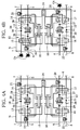
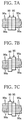
switches 81 - 84 is shown in FIGs. 7A-7C. Unlike the switch
architecture of FIGs. 2A and 2B, this architecture provides
for three switching states, corresponding to each of the FIGs.
7A-7C. As shown in FIG. 7A, a first ferrule 90 and a second
ferrule 95 are aligned at their alignment side end surfaces.
Also, a refractive index matching oil (not shown) is used to
fill in the gap between the alignment side end surfaces of
these ferrules 90 and 95. Further, the optical switches 81
- 84, which are used in this embodiment of the present
invention, is electrically switched by use of the pins (not
shown) that are driven by a solenoid coil. The pins (not
shown) can be manually moved if a knob is provided at a
member for connecting the pin and the coil, whereby the
switching operation can be performed even in an emergency
such as an interruption of service. It is therefore feasible
to provide the optical line switching system with high
reliability.
The first and second ferrules 90 and 95 each have six
strands of optical fibers (e.g., 90a and 95a) that are
equally spaced. The switching states shown in FIGs. 7A-7C
are denoted state I, state II, and state III, respectively.
In FIG. 6A, all of the four optical switches 81-84 are in
switching state I. Any one of the optical switches 81-84 can
transition from state I (which is a default state) to state
II or state III by a single movement of the second ferrule
95; i.e., by one single switching operation. State II is
achieved by moving the second ferrule 95 up one fiber spacing.
Further, a state I to state III occurs when the second
ferrule 95 is moved downward.
The operation of the optical switches 81-84 to invoke
the protection functions of a ring protection scheme and a
span protection scheme is described with respect to FIG. 6B.
If faults Os occur in the working optical fibers 5 and 6 and
in the protection optical fiber 7, the ECU 24, based on the
signals outputted from the photo diodes 19 and 20 and a photo
diode in node N-1 (not shown), sets up alternate transmission
paths. The ECU 24 transmits control signals to optical
switches 81 and 84 to alter their switching states, from
state I to state II.
To overcome the faults on optical fibers 5 and 7,
traffic on protection optical fiber 7 is redirected to
working optical fiber 5. This alternative transmission path
reroutes optical signals from node N-1 (not shown) that are
carried over protection fiber 7. Optical switch 82, which is
in state I, receives the optical signals and forwards them to
optical switch 81, which is in state II, via optical
amplifier 30.
The alternative transmission path from fiber 7 to fiber
5 requires three optical amplifiers 30, 26 and 28. Optical
amplifier 30 compensates for transmission loss associated
with the propagation of the optical signals over the
protection optical fiber 7 from the adjacent node, N-1.
Further, under normal operation (as described in Figure 6A),
low priority data is carried over the protection fiber 7, in
which case optical amplifier 30 is needed to boost the
corresponding degraded optical signals. Next, optical switch
81 switches the optical signals out a port that is connected
to an optical amplifier 26. Optical amplifier 26 compensates
for transmission loss as well as loss that is introduced by
the optical signal processing unit 11. The optical signal
processing unit 11 divides the optical signal into the
respective wavelengths, thereby reducing the signal strength
of the optical signals. After the optical add/dropped is
executed by the optical signal processing unit 11, optical
amplifier 28 amplifies the resultant optical signals for
transmission to the adjacent node.
The optical signal processing unit 11, in turn, sends
the resultant optical signals back to optical switch 82
through optical amplifier 28. Optical amplifier 28 boosts
the optical signals up for transmission to adjacent node N+1
(not shown). The optical switch 82 transmits the optical
signals over working fiber 5. The above alternate
transmission path follows a ring protection scheme.
It should be noted that although the optical signals
pass through only two optical amplifiers 26 and 28 in the
normal state, they also pass through the optical amplifier 30
under the ring protection scheme. Therefore, in order to
cancel the gain of the optical amplifier 30, it is necessary
that the optical signals pass through optical attenuators 34
and 35, depending on the location of the fault. Consequently,
the optical attenuators 34 and 35 are designed to offset
collectively the gain of optical amplifier 30. Because the
gain of optical amplifier 30 is known, the attenuation amount
can be fixed. In contrast, the optical attenuators 38 and 39
of the embodiment 2 (Figs. 4A and 4B), a variable attenuator
is used, in which the amount of attenuation is set to zero in
the normal state and some attenuation level equal to the
optical amplifier during execution of the ring protection
scheme. One of ordinary skill in the art would recognize
that if the distance between the adjacent nodes is short or
the optical processing devices exhibit low loss, optical
amplifiers may not be required.
As for the fault on working fiber 6 on the right side of
node N 45, optical switch 84 switches the optical signals
from protection fiber 8 to optical signal processing device
12 via optical amplifier 27. The operation of optical
amplifiers 31, 27, and 29 are identical to that of optical
amplifiers 30, 26, and 28, respectively. These optical
amplifiers 31, 27, and 29 operate with respect to optical
switches 83 and 84 and optical processing device 12. The
optical signal processing device 12 sends the optical signals
to optical amplifier 29, which forwards the optical signals
to optical switch 83. In turn, optical switch 83 sends the
optical signals over working fiber 6. The above switch
configuration implements the span protection scheme.
As discussed above, the working and protection optical
fibers pairs 5/7, and 6/8 independently perform the
protection functions according to the ring and span
protection schemes, depending on the position of the fiber
fault. Table 3 lists the optical fiber fault positions in
relation to the switching states of the optical switches.
| Switching States of Optical Switches | Optical Fiber Fault Positions |
| 81 | 82 | 83 | 84 |
| I | I | I | I | Fault free condition |
| I | II | III | I | Faults occurred both in working and protection fibers on downstream side of node (ring protection scheme) |
| II | I | I | III | Faults occurred both in working and protection fibers on upstream side of node (ring protection scheme) |
| II | I | I | II | Fault occurred in working fiber on upstream side of node (span protection scheme) |
| I |
| I | III | II | I | Fault occurred in working fiber on downstream side of node (span protection scheme) |
| II | III | II | II | Faults occurred in working fibers on both of upstream side and downstream side of node (span protection scheme) |
| I |
As evident from Table 3, in most cases the protection
function is invoked by changing only one optical switch. For
example, when faults occurred both in working and protection
fibers on the downstream-side of the node (as in the second
column of Table 3), the optical switch 82 transitions to
state II; however, switch 81 does not need to transition
state. Therefore, according to the optical line switching
system 45, there is a reduced probability of not invoking the
optical protection function resulting from a failure to
switch the optical switch. In other words, the fewer the
number of switches that need to transition, the less
likelihood that a switch malfunction will occur.
Based on the foregoing discussion, the number of optical
switches in the optical line switching systems, as
exemplified in Embodiments 1-4, can be reduced.
Embodiment 5
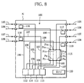
An optical line switching system 100, according to yet
another embodiment of the present invention is illustrated in
FIG. 8. The optical line switching system 100 is a node N
within an optical communications network, which utilizes
working optical fibers 105 and 106 and protection optical
fibers 107 and 108. Node N 100 can be configured as part of
a ring network with adjacent node N-1 (to the left) and node
N+1 (to the right). Node N 100 includes four optical signal
processing devices 111-114 (e.g., OADMs), which are connected
to a single 4x4 optical switch 115. Monitoring devices 116-119
(i.e., photo diodes) provide information about fault
conditions of optical fibers 105-108. respectively, to
electronic control unit (ECU) 120. The ECU 120 controls the
4x4 optical switch 115 to effect the ring protection scheme
and the span protection scheme.
The photo diodes 116-119 receive input optical signals
into node N 100 from working optical fibers 105 and 106 and
protection optical fibers 107 and 108 to monitor whether a
fault has occurred on any of these optical fibers 105-108.
That is, the photo diodes 116-119 are situated within the
node N 100 so that they measure the power levels of the
optical signals entering the node N 100 (i.e., optical
signals that are transmitted from nodes N-1 and N+1).
Although not shown, each of the photo diodes 116-119 is
connected to ECU 120; in addition, photo diodes 116-119 may
also output monitoring signals to an electronic control unit
that resides in an adjacent node, depending on the
implementation of the monitoring system.
The ECU 120 controls the switching operation of the 4x4
optical switch 115. Based on the power levels of the optical
signals transmitted from the photo diodes 116-119, the ECU
120 determines whether a fault exists by comparing these
power levels with a predetermined value. If the power levels
are at or below this predetermined value, then one or more of
the optical fibers 105-108 is faulty; and the ECU 120 outputs
a control signal to the 4x4 optical switch 115 to change its
switching state to effect a protection scheme.
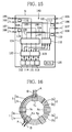
FIG. 8 illustrates a fault free condition, whereby all
the optical fibers 105-108 are properly functioning - i.e.,
can carry traffic. Focusing on the right side of node N 100,
optical signals are transmitted out of node N to node N+1
(not shown) over working optical fiber 105 and protection
optical fiber 107. Working optical fiber 106 and protection
optical fiber 108 deliver traffic to node N from node N+1
(not shown). From the perspective of the left side of node N,
the working fiber 105 and protection fiber 107 carry optical
signals into node N from node N-1 (not shown). Further,
working fiber 106 and protection optical fiber 108 transport
optical signals from node N-1 to node N 100.
The optical signal processing devices 111-114, as shown
in FIG. 8, performs an optical add/drop function of adding
and dropping the necessary optical signals without the need
to perform electrical conversion of the optical signals.
Particularly in a WDM system, the optical signal processing
devices 111-114 temporarily demultiplexes the composite
optical signals; after which the individual optical signals
with the proper wavelengths are added and dropped.
Subsequently, the individual optical signals are optically
multiplexed to form a new composite optical signal. A fiber
Bragg grating (FBG) can be used as the optical signal
processing device. Furthermore, the optical signal
processing devices 111-114 possess optical cross-connect
functionality to switch the optical signals in and out of the
ring network. The optical cross-connect capability, for
example, can be supplied by the optical switch 115. Optical
amplifiers (not shown) are disposed before and after each of
the optical signal processing devices 111-114. Because of
the low loss of optical switch 115, these optical amplifiers
(not shown) need not provide high signal amplification, which
advantageously permits use of inexpensive optical amplifiers.
As shown in FIG. 8, the 4x4 optical switch 115 has four
input ports PI1-PI4 and four output ports PO1-PO4. The 4x4
optical switch 115 is connected to the optical signal
processing devices 111-114. Under the fault free condition
of FIG. 8, the input port to output port bar-state (i.e.,
connection states) of the 4x4 optical switch 115 is as
follows: port PI1 to port PO1, port PI2 to port PO2, port PI3
to port PO3, and port PI4 to port PO4.
To effect the necessary optical protection functions, it
is not necessary to utilize a non-blocking switch. That is,
the 4x4 optical switch 115 need not exhibit non-blocking
connections between the input ports PI1-PI4 and the output
ports PO1-PO4. However, a one-to-one correspondence between
the input ports and the output ports is required in a fault
free condition. In the case of a fault, a predetermined
connection between the working optical fibers 105 and 106 and
the protection optical fibers 107 and 108 needs to be
established. Thus, in some applications, it may suffice that
some blocking occur within the 4x4 optical switch 115,
thereby reducing switching cost.
According to an exemplary embodiment, the 4x4 optical
switch 115 can be constructed of two interlocking type
optical switches SWA and SWB as shown in FIG. 9. Optical
switches SWA and SWB form a common switching fabric. Further,
each of the interlocking type optical switches SWA and SWB is
made by combining two 2x2 type unit optical switches SWU. A
2x2 type unit optical switch SWU has two input ports and two
output ports, as denoted by the circles. A common driving
mechanism drives the two unit optical switches SWU. In this
manner, it is feasible to simultaneously perform switching
operation of the unit optical switches SWU to change the
switching states of the optical switches SWA and SWB.
Optical fibers, Fop, connect to the optical switches SWA and
SWB. The ports PO1-PO4 and PI1-PI3 of the collective 4x4
optical matrix switch are shown as squares.
The 4x4 matrix optical switch 115, according to this
embodiment of the present invention, advantageously has low
insertion loss. Based upon experimentation, the interlocking
type optical switches with the structures shown in FIGs. 2A
and 2B exhibit typical insertion loss values around 0.3dB.
The insertion loss of the 4x4 matrix optical switch 115 is
about 0.6dB. Because of this low loss characteristics,
optical amplifiers, which are expensive, are not required to
offset loss that is attributable by the 4x4 matrix optical
switch.
FIG. 10 shows the occurrence of faults Os in the working
optical fibers 105 and 106 and the protection optical fibers
107 and 108 on the left side of node N 100. In this scenario,
the photo diodes 116 and 118 within node N 100 transmit
monitoring signals, which indicate the power levels of the
optical signals that carried over working optical fiber 105
and protection optical fiber 107, to ECU 120. The ECU 120
also receives signals from photo diodes that reside in the
left adjacent node N-1 and that correspond to working optical
fiber 106 and protection optical fiber 108. Node N 100 thus
needs to effect the ring protection scheme. To recover from
these faults, ECU 120 outputs control signals to the 4x4
optical switch 115, resulting in the following connection
states (i.e., I/O port mapping): port PI1 to port PO4, port
PI2 to port PO3, port PI3 to port PO2, and port PI4 to port
PO1.
As a result, two alternate transmission paths are
created, as indicated by the bold lines. First, optical
signals that are transmitted over working optical fiber 106
(from node N+1) are sent to optical signal processing device
112, which forwards the processed optical signals to optical
switch 115 at port PI1. The optical switch 115 then outputs
the optical signals via port PO4 onto protection optical
fiber 107. Secondly, optical signals that enter node N 100
via protection optical fiber 108 are handled by optical
signal processing device 114. After processing the received
optical signals, optical signal processing device 114 sends
them to port PI2 of optical switch 115; the optical switch
115 then transmits the optical signals out of port PO3 over
working optical fiber 105.
The above scenario concerned failures of all four
working and protection fibers on the left side of node N 100,
whereby the ring protection function was effected to
establish the alternative transmission paths. If the link
failures occurred on the right side of the node N 100, a ring
protection function is effected by ECU 120 in conjunction
with optical switch 115. In this case, the determination by
ECU 120 of whether and where faults have occurred is based
upon the monitoring signals that are outputted from the photo
diodes (not shown) contained in the adjacent right node N+1
(not shown) corresponding to optical fibers 105 and 107. In
addition, ECU 120 receive inputs from photo diodes 117 and
119 within node N 100. Because the power levels of the
optical signals that have been transported over optical
fibers 105-108 experience a reduction in intensity, ECU 120
outputs a control signal to optical switch 115, thereby,
changing the switching state of the switch 115 to the same
state as described in FIG. 10.
FIG. 11 shows a fault condition requiring use of the
span protection scheme, in which faults Os occur in the
working optical fibers 105 and 106 on the left side of the
node N. To recover from fault Os, ECU 120 outputs a control
signal to 4x4 optical switch 115 in response to monitoring
signals from the photo diode 116 within node N 100 and from a
photo diode (not shown) that corresponds to working optical
fiber 106 and is situated in the adjacent left node N-1 (not
shown). Upon receiving the control signal from ECU 120, the
4x4 optical switch 115 changes its switching state to the
following mapping: port PI1 to port PO2, port PI2 to port PO1,
port PI3 to port PO4, and the port PI4 to port PO3.
The resultant alternate paths are shown as bold lines.
The optical signals, which are transmitted via the working
optical fiber 106, enter node N 100 from adjacent right node
N+1 (not shown) and are processed by optical signal
processing device 112. Subsequently, optical signal
processing device 112 transmits the optical signals to port
PI1 of the 4x4 optical switch 115. In turn, the switch 115
sends the optical signals over optical fiber 108 through port
PO2. Under non-fault conditions, optical switch 115 would
have transmitted the optical signals out of port PO1. Thus,
in the alternative transmission path, optical signals that
enter node N over working optical fiber 106 (on the right
side) are switched to protection optical fiber 108, thus
rerouting around the faulty link 106 (on the left side).
Another alternative path is devised for optical signals
carried by protection optical fiber 107 into node N 100 from
the adjacent left node N-1. Upon entering the node N 100,
these optical signals are sent to optical signal processing
device 113, which forwards the optical signals to optical
switch 115 at port PI4. The optical switch 115, in the new
switching state, switches the optical signals out through
port PO3 and unto working optical fiber 105 for transport to
the adjacent right node N+1.
In the above discussion of FIG. 11, the span protection
scheme involved faults Os occurring on the left side of
node
N 100. However, in the case where the fault Os affect the
right side of
node N 100, a similar recovery mechanism is
invoked by
ECU 120.
ECU 120 receives monitoring signals from
photo diode 117 within
node N 100 and from a photo diode that
corresponds to
optical fiber 105 and resides on the adjacent
right node N+1 (not shown). Upon determination of an
occurrence of fault Os on working
optical fibers 105 and 106
(on the right side of node N 100),
ECU 120 correspondingly
generates a control signal to
optical switch 115 to change
switching state. The switching state, in this scenario, is
identical to the switching state that resulted from the
faults Os of FIG. 11. Table 4 lists the relationship between
the optical fiber fault positions and the switching states of
the optical switches during implementation of the various
protection functions.
| Switching States of Interlocking Type Optical Switches | Connection States of Ports in 4x4 Optical Switch 115 | Working Protection Function |
| SWA | SWB |
| bar-state | bar-state | PI1-PO1, PI2-PO2, PI3-PO3, PI4-PO4 | Fault free condition |
| cross-state | bar-state | PI1-PO4, PI2-PO3, PI3-PO2, PI4-PO1 | Ring protection |
| bar-cross | cross-state | PI1-PO2, PI2-PO1, P13-PO4, PI4-PO3 | Span protection |
The 4x4 optical switch 115 used in the optical line
switching system 100, according to Embodiment 5 of the
present invention, has the capability to implement the ring
protection scheme by changing the switching state of only one,
namely SWA, of the interlocking type optical switches SWA,
SWB from the bar-state to the cross-state. To implement the
span protection scheme, only the interlocking type optical
switch SWB of the two interlocking type optical switches SWA
and SWB, which constitute the 4x4 optical switch 115, changes
its switching state from the bar-state to the cross-state.
Thus, the switching state of the 4x4 optical switch can be
altered by applying a voltage to only some of the unit
optical switches that make up the 4x4 optical switch 115. In
contrast, the conventional 4x4 optical switch, which includes
multiple unit switches, requires supplying a voltage to all
the unit switches, when changing the switching state of the
conventional 4x4 optical switch. The arrangement of
Embodiment 5 of the present invention advantageously reduces
power consumption. Power efficiency is also realized by the
fact that a switching state is maintained without the need to
supply power.
In the optical line switching system 100, the use of two
optical switches SWA and SWB provides high reliability,
thereby avoiding misconnections resulting from switch failure.
In addition, the optical switches SWA and SWB exhibit smaller
insertion loss than the conventional 4x4 optical switch.
Embodiment 6
As shown in FIG. 12, an optical line switching system
130 has, in accordance to another embodiment of the present
invention, two optical switches 122 and 123 that are
connected to optical switch 115. These two optical switches
122 and 123 are located between optical switch 115 and the
optical signal processing devices 111-114. Each of the
optical switches 122 and 123 can be implemented using the
switch architecture of FIG. 9. That is, the optical switches
122 and 123 include interlocking type optical switches SWA
and SWB, with input ports PI1-PI4 and output ports PO1-PO4
(see FIGs. 13A-13C). The optical switches shown in FIGs. 2A
and 2B are usable as the interlocking type optical switches
SWA and SWB.
The optical line switching systems, as explained in this
embodiment and subsequent embodiments, have basically the
same architecture as the optical line switching system 100 of
Embodiment 5, with the exception of additional optical
switches; e.g., optical switches 122-124. For purpose of
explanation, only optical switch 122 and the optical signal
processing devices 112 and 114, which are defined by the
dotted line in FIG. 12, are discussed, as the operation of
optical switch 123 in conjunction with optical signal
processing devices 111 and 113 are similar. Optical switch
122 has port arrangement shown in FIGs. 13A-13C, which are
also applicable to optical switch 123.
Accordingly, FIGs. 13A-13C and Table 5 show the port
mappings of optical switch 122 associated with the various
switching states of the interlocking type optical switches
SWA, and SWB. In the optical line switching system 130, if
both of the interlocking type optical switches SWA and SWB
are in the bar-state, any received optical signals are not
forwarded to the optical signal processing devices 112 and
114 (as shown in FIG. 13A). Optical signals that are
transmitted via the working optical fiber 106 and the
protection optical fiber 108 are switched by the optical
switch 122 to bypass optical signal processing devices 112
and 114. Specifically, optical signals associated with
optical fiber 106 enter port PI4 of optical switch 122 and
are forwarded out of port PO4. In this switching state,
optical switch 122 receives optical signals from optical
fiber 108 at port PI2 and outputs these signals through port
PO2. Consequently, these optical signals are simply
transferred by 4x4 optical switch 115 to an adjacent node
(e.g., node N-1 or node N+1).
FIG. 13B reflects a switching state, whereby the
interlocking type optical switch SWA is in the cross-state.
In this scenario, optical signals that are carried over
optical fibers 106 and 108 are sent to optical signal
processing devices 112 and 114 by the optical switch 122.
That is, the optical switch 122 receives optical signals from
optical fiber 106 at port PI4 and transmits them out of port
PO1 to optical signal processing device 112. After the
optical signals are processed by optical signal processing
device 112, optical signal processing device 112 sends the
processed signals back to optical switch 122 at port PI1.
The optical switch 122, subsequently, switches the optical
signals out port PO4 to an adjacent node (e.g., node N-1 or
node N+1) via the 4x4 optical switch 115. In a similar
manner, optical signals that are transmitted into optical
switch 122 via protection optical fiber 108 are switched from
port PI2 to port PO3 to optical signal processing device 114,
which sends the optical signals back to optical switch 122 at
port PI3, after the optical signals are processed by optical
signal processing device 114. In turn, optical switch 122
switches the optical signals, which are destined to an
adjacent node (not shown) via the 4x4 optical switch 115, out
port PO2.
As illustrated in FIG. 13C, if the optical
signal
processing device 112 fails, switch SWB can be changed to the
cross-state. Accordingly, optical signals from
optical fiber
106 are switched by
optical switch 122 from port PI4 to port
PO3, which is connected to optical
signal processing device
114. The optical signals are processed by optical
signal
processing device 114, which sends the optical signals back
to
optical switch 122 at port PI3. In turn,
optical switch
122 switches the optical signals, which are destined to an
adjacent node (not shown) via the 4x4
optical switch 115, out
port PO4..
| Switching States of Interlocking Type Optical Switches | Connection States of Ports in Optical Switch 122 | Bypass of Optical Signal Processing Devices 112 and 114 |
| SWA | SWB |
| bar-state | bar-state | PI1-PO1, PI2-PO2, PI3-PO3, PI4-PO4 | Bypassed | FIG 13A |
| cross-state | bar-state | PI1-PO4, PI2-PO3, PI3-PO2, PI4-PO1 | Not bypassed | FIG. 13B |
| bar-state | cross-state | PI1-PO2, PI2-PO1, PI3-PO4, PI4-PO3 | Not bypassed (failure of optical signal processing device 112) | FIG. 13C |
Although the above discussion of Embodiment 6
specifically describes use of a 4 x 4 optical switch (shown
in FIG. 9), other types of optical switches may be employed.
In an alternative approach, the interlocking optical switch
of FIGs. 2A and 2B may be used as the optical switches 122
and 123. In this alternative approach, the optical line
switching system determines whether the wavelength-multiplexed
optical signals pass through the optical signal
processing devices 112 and 114 based upon the switching
states of the interlocking type optical switches. For
example, if the interlocking optical switches are in a bar-state,
the optical signal processing devices 112 and 114 are
bypassed; however, with the interlocking optical switches in
the cross-state, the optical signals are sent through the
optical signal processing devices 112 and 114.
Embodiment 7
FIG. 14 shows an optical line switching system 135, in
accordance with another embodiment of the present invention,
that employs an additional optical switch over the system of
Embodiment 5 in a manner that permits usage of any one of the
optical signal processing devices in the event of failure of
one or more of them. Optical switch 124, which is connected
to optical signal processing devices 111-114, possesses a
switch architecture as shown in FIG. 9. Further, the optical
switch 124 includes interlocking type optical switches SWA
and SWB and has input ports PI1-PI4 and output ports PO1-PO4,
as illustrated in FIG. 14.
Table 6 shows the relationship among the following
parameters: switching states of the optical switches, port
mappings associated with the switching states, optical
processing device failure, and optical fiber fault condition.
| Switching States of Interlocking Type Optical Switches | Connection States of Ports in 4x4 Optical Switch 124 | Breakdown in Optical Signal Processing Device | States of Faults in Optical Fibers |
| SWA | SWB |
| bar-state | bar-state | PI1-PO1 PI2-PO2, PI3-PO3 PI4-PO4 | no breakdown | No fault |
| cross-state | bar-state | PI1-PO4 PI2-PO3, PI3-PO2, PI4-PO1 | breakdown | Faults in working and protection optical fibers |
| bar-state | cross-state | PI1-PO2, PI2-PO1, PI3-PO4, PI4-PO3 | breakdown | Fault in working optical fiber. |
| cross-state | cross-state | PI1-PO3 PI2-PO4, PI3-PO1 PI4-PO2 | breakdown | No fault |
As shown in FIG. 15, an optical line switching system
140 in Embodiment 8 is constructed by adding an optical
switch 124 to the optical line switching system 130 of
Embodiment 6. Under this arrangement, optical switch 124
connects to optical switches 122 and 123. The optical line
switching system 140 is able to recover from a variety of
faults in the transmission lines (e.g., optical fibers 105-108),
as well as equipment (e.g., optical signal processing
devices 111-114) by creating alternative routes for the
optical signals.
In accordance with each of the Embodiments 5-8, optical
switch 115, which is provided on the downstream of optical
signal processing devices 111-114, operates to implement
fault recovery stemming from faults within working optical
fibers 105 and 106 and protection optical fibers 107 and 108.
Located upstream from optical signal processing devices 111-114,
optical switches 122, 123, and 124 serve to supply the
capability to bypass optical signal processing devices 111-114
and to direct traffic to an operable optical signal
processing device (e.g., 111-114).
It should be noted that each of the optical line
switching systems in the respective embodiments, as discussed
above, has been explained with respect to WDM optical signals.
However, these embodiments have applicability to code
division multiplexed optical signals as well as time division
multiplexed optical signals.
Additionally, in each of the embodiments discussed above,
the photo diodes provided in the intra-node transmission path
directly monitors the optical signals or some of them,
thereby detecting whether a fault has occurred in the
transmission path. The device for detecting such faults is
not limited to the embodiments described above. The
occurrence of the fault may be detected by use of, for
example, a pilot tone detecting circuit, which is provided in
the node. Such a circuit is described in Journal of Light
wave Technology, Vol.15, No.12, Dec., 1997, pp.2197-2205,
Yoshiyuki Hamazumi and Masafumi Koga, "Transmission Capacity
of optical Path Overhead Transfer Scheme Using Pilot Tone for
Optical Path Network", which is herein incorporated by
reference.
The techniques described herein provide several
advantages over prior approaches to implementing an optical
protection scheme, such as the ring and span protection
mechanisms. The optical communications network are populated
with nodes that introduce high network reliability. As
explained, the nodes utilize optical switches, in which each
optical switch includes dual unit optical switches that have
a common driving mechanism. The common driving mechanism is
configured to perform simultaneously switching operation of
the unit optical switches to alter a switching state of the
optical switch. Monitoring devices are used to detect faults
by outputting monitoring signals that indicate one or more
faults in the working optical fibers and the protection
optical fibers. A control device, in response to monitoring
signals, outputs control signals to the optical switches to
invoke an optical protection scheme. The control signals
instruct the optical switches to change switching states.
Therefore, the present invention presents an efficient and
economically feasible approach to recover from link failures
as well as intra-node equipment failure.
Obviously, numerous modifications and variations of the
present invention are possible in light of the above
teachings. It is therefore to be understood that within the
scope of the appended claims, the invention may be practiced
otherwise than as specifically described herein.
Where technical features mentioned in any claim are followed by reference signs, those
reference signs have been included for the sole purpose of increasing the intelligibility
of the claims and accordingly, such reference signs do not have any limiting effect on
the scope of each element identified by way of example by such reference signs.