EP1037330A2 - Impedance tuning in electrical switching connector - Google Patents
Impedance tuning in electrical switching connector Download PDFInfo
- Publication number
- EP1037330A2 EP1037330A2 EP00105058A EP00105058A EP1037330A2 EP 1037330 A2 EP1037330 A2 EP 1037330A2 EP 00105058 A EP00105058 A EP 00105058A EP 00105058 A EP00105058 A EP 00105058A EP 1037330 A2 EP1037330 A2 EP 1037330A2
- Authority
- EP
- European Patent Office
- Prior art keywords
- terminals
- switch
- connector
- ground
- ground terminal
- Prior art date
- Legal status (The legal status is an assumption and is not a legal conclusion. Google has not performed a legal analysis and makes no representation as to the accuracy of the status listed.)
- Withdrawn
Links
Images



Classifications
-
- H—ELECTRICITY
- H01—ELECTRIC ELEMENTS
- H01R—ELECTRICALLY-CONDUCTIVE CONNECTIONS; STRUCTURAL ASSOCIATIONS OF A PLURALITY OF MUTUALLY-INSULATED ELECTRICAL CONNECTING ELEMENTS; COUPLING DEVICES; CURRENT COLLECTORS
- H01R13/00—Details of coupling devices of the kinds covered by groups H01R12/70 or H01R24/00 - H01R33/00
- H01R13/66—Structural association with built-in electrical component
- H01R13/70—Structural association with built-in electrical component with built-in switch
- H01R13/703—Structural association with built-in electrical component with built-in switch operated by engagement or disengagement of coupling parts, e.g. dual-continuity coupling part
- H01R13/7031—Shorting, shunting or bussing of different terminals interrupted or effected on engagement of coupling part, e.g. for ESD protection, line continuity
-
- H—ELECTRICITY
- H01—ELECTRIC ELEMENTS
- H01R—ELECTRICALLY-CONDUCTIVE CONNECTIONS; STRUCTURAL ASSOCIATIONS OF A PLURALITY OF MUTUALLY-INSULATED ELECTRICAL CONNECTING ELEMENTS; COUPLING DEVICES; CURRENT COLLECTORS
- H01R13/00—Details of coupling devices of the kinds covered by groups H01R12/70 or H01R24/00 - H01R33/00
- H01R13/646—Details of coupling devices of the kinds covered by groups H01R12/70 or H01R24/00 - H01R33/00 specially adapted for high-frequency, e.g. structures providing an impedance match or phase match
- H01R13/6473—Impedance matching
-
- H—ELECTRICITY
- H01—ELECTRIC ELEMENTS
- H01R—ELECTRICALLY-CONDUCTIVE CONNECTIONS; STRUCTURAL ASSOCIATIONS OF A PLURALITY OF MUTUALLY-INSULATED ELECTRICAL CONNECTING ELEMENTS; COUPLING DEVICES; CURRENT COLLECTORS
- H01R13/00—Details of coupling devices of the kinds covered by groups H01R12/70 or H01R24/00 - H01R33/00
- H01R13/648—Protective earth or shield arrangements on coupling devices, e.g. anti-static shielding
- H01R13/658—High frequency shielding arrangements, e.g. against EMI [Electro-Magnetic Interference] or EMP [Electro-Magnetic Pulse]
- H01R13/6581—Shield structure
- H01R13/6585—Shielding material individually surrounding or interposed between mutually spaced contacts
-
- H—ELECTRICITY
- H01—ELECTRIC ELEMENTS
- H01R—ELECTRICALLY-CONDUCTIVE CONNECTIONS; STRUCTURAL ASSOCIATIONS OF A PLURALITY OF MUTUALLY-INSULATED ELECTRICAL CONNECTING ELEMENTS; COUPLING DEVICES; CURRENT COLLECTORS
- H01R2201/00—Connectors or connections adapted for particular applications
- H01R2201/02—Connectors or connections adapted for particular applications for antennas
-
- H—ELECTRICITY
- H01—ELECTRIC ELEMENTS
- H01R—ELECTRICALLY-CONDUCTIVE CONNECTIONS; STRUCTURAL ASSOCIATIONS OF A PLURALITY OF MUTUALLY-INSULATED ELECTRICAL CONNECTING ELEMENTS; COUPLING DEVICES; CURRENT COLLECTORS
- H01R2201/00—Connectors or connections adapted for particular applications
- H01R2201/24—Connectors or connections adapted for particular applications for radio transmission
Definitions
- This invention generally relates to the art of electrical connectors and, particularly, to a method of tuning the characteristic impedance of an electrical switching connector.
- Radio frequency electrical connectors are used in a wide variety of applications. Such connectors are used in mobile telephones, global positioning systems and the like. Basically, such a connector is a microwave connector.
- Such connectors is an electrical switching connector used in a transceiver of such devices which requires an antenna, such as a mobile telephone.
- the transceiver may be normally connected to an internal antenna, and switching terminals are provided for connecting the unit to an external antenna.
- the switching terminals are normally closed, and a terminal from a coaxial cable opens the normally closed terminals to disconnect the transceiver from the internal antenna and connect the transceiver to the external antenna.
- ground terminals also are employed in conjunction with the switching terminals.
- an ideal connector would be "transparent". In other words, the system would function as if circuitry ran through the interconnection and there would be no affect on the system whatsoever. However, such an ideal connector is impractical or impossible, and continuous efforts are made to develop an electrical connector which has as little affect on the system as possible.
- Impedance and inductance control are concerns in designing an ideal connector.
- an ideal connector would have little or no affect on the interconnection system regarding these characteristics. This is particularly true in radio frequency connectors as described above.
- the invention herein is directed to a method for tuning the impedance of an electrical connector, such as an electrical switching connector. It should be understood that the concepts of the invention as disclosed and claimed herein are not limited to radio frequency connectors in that the invention has a wide range of advantageous applications.
- An object, therefore, of the invention is to provide a new and improved method of tuning the characteristic impedance of an electrical connector, such as an electrical switching connector.
- the method comprises the steps of providing a pair of switch terminals having operatively engageable contact portions.
- a pair of ground terminals are juxtaposed alongside the switch terminals.
- the method includes the step of adjusting the spacing between at least one of the ground terminals and one of the switch terminals to adjust the capacitance therebetween and, thereby, adjust the impedance of the connector.
- the contact portion of the switch terminal is elongated
- the one ground terminal includes an elongated leg generally parallel to the contact portion of the one switch terminal.
- the adjusting step comprises adjusting the spacing between the elongated contact portion and the elongated leg.
- the pair of ground terminals are shown herein in the form of the legs of a generally U-shaped configuration.
- the ends of the legs are integrally joined by a cross portion of the U-shaped configuration.
- the invention contemplates tuning the connector by adjusting the spacing between the cross portion and an end of one of the switch terminals.
- the impedance also can be tuned by varying the size of the cross portion to adjust the impedance of the ground terminals.
- the invention also contemplates that at least a portion of the one of the switch terminals overlaps at least a portion of one of the ground terminals.
- the overlapping area can be adjusted to adjust the capacitance between the terminals and, thereby, adjust the impedance of the connector.
- the invention also contemplates overmolding a dielectric housing about at least portions of the ground terminals and the one switch terminal after the adjusting step(s).
- Such an overmolding step precisely fixes the terminals in their relative positions of adjustment. Therefore, nothing has to be changed in the size or shape of the connector or the connector housing to provide different connectors with different impedance characteristics which is accomplished simply by adjusting the location of the terminals within the mold in which the housing is overmolded about the terminals.
- an electrical switching connector generally designated 12, which includes a one-piece housing, generally designated 14.
- the housing is unitarily molded of dielectric material such as plastic or the like.
- the housing has a bottom mounting surface 16 for mounting the connector on the surface of a printed circuit board (not shown).
- the housing has a rear terminating end 18 (Fig. 1) and a front receptacle end 20 defining a receptacle 22 (Fig. 2) which receives at least a terminal blade of a complementary mating connector, such as for a coaxial cable coupled to an external antenna.
- switching connector 12 includes a first switch terminal, generally designated 24; a second switch terminal, generally designated 26; a first ground terminal, generally designated 28; and a second ground terminal, generally designated 30. All of the terminals are stamped and formed of conductive sheet metal material. All of the terminals 24-30 have coplanar tail portions 24a-30a, respectively, for connection to appropriate power and ground circuit traces on the printed circuit board, as by soldering.
- First switch terminal 24 is the "switched" terminal of the connector and includes an elongated body portion 24b extending through housing 14 and including a widened distal end 24c defining a contact portion located at receptacle 22 of the housing.
- Ground terminals 28 and 30 also have elongated body portions 28b and 30b, respectively, extending forwardly in the housing on opposite sides of the body portion 24b of switch terminal 24.
- Body portion 30b of ground terminal 30 is wider than body portion 28b of ground terminal 28 and includes a cut-out area 30c for accommodating the widened contact portion 24c of switch terminal 24. All of the body portions 24b, 28b and 30b of the respective switch and ground terminals are generally coplanar.
- Second switch terminal 26 is a "common" or power terminal of the connector and has an elongated body portion 26b which is elevated in a plane above the plane of the body portions of the other terminals.
- the body portion of the second switch terminal is flexible and has a downwardly projecting, bowed contact portion 26c which is normally in engagement with contact portion 24c of first switch terminal 24 to provide a normally closed switch for connector 12.
- transition portions 24d, 28d and 30d of switch terminal 24 and ground terminals 28 and 30, respectively, along with at least portions of the body portions of those terminals, are overmolded by molded plastic housing 14 to rigidify the terminals and maintain the terminals in precise position and spacing. This can be done easily in a molding die.
- second switch terminal 26 is inserted into a slot 32 at the rear of the housing so that body portion 26b of the terminal is free to flex relative to body portion 24b of the first switch terminal 24.
- the second switch terminal has an enlarged plate portion 26d which is insertable into slot 32 of the housing.
- a pair of rounded locking bosses 26e provide an interference fit within slot 32 to hold switch terminal 26 in the housing.
- body portion 28b and 30b of ground terminals 28 and 30 respectively, form the legs of a generally U-shaped configuration, with the ends of the legs being integrally joined by a cross portion 34 of the U-shaped configuration. Therefore, the unitary U-shaped ground terminal structure surrounds body portion 24b and contact portion 24c of first switch terminal 24.
- cross portion 34 of the ground terminal structure has a downwardly turned lip 34a and widened contact portion 24c of first switch contact 24 also has a downwardly turned lip 24d.
- Figure 5 is a duplicate of Figure 4 and simply highlights an area 36 whereat plate portion 26d of second switch terminal 26 overlaps body portion 30b of ground terminal 30. This overlapping area provides an increase in the capacitor area between those terminals which, in turn, lowers the characteristic impedance of the connector.
- FIG. 6 shows a terminal blade 38 of a complementary mating connector inserted into connector 12 and into engagement with contact portion 26c of second switch terminal 26. This lifts contact portion 26c off of contact portion 24c of first switch terminal 24 and, thereby, opens the switch therebetween.
- switching connector 12 may be a transceiver connector in a mobile telephone unit, for instance.
- the unit will have an internal antenna which is connected to switch terminal 24 and which is normally coupled in circuit by the normally closed switch terminals 24 and 26.
- Terminal blade 38 (Fig. 6) may be from a coaxial cable coupled to an external antenna. Therefore, when blade 38 engages contact portion 26c of switch terminal 26 to "open" the switch of connector 12, the engagement of blade 38 with second switch terminal 26 now disengages the connector from the internal antenna and couples the connector to the external or outside antenna.
- Figures 7-10 show an alternate embodiment of the invention and like numerals have been applied in Figures 7-10 corresponding to like components described above in relation to Figures 1-6.
- the main difference between the embodiment of Figures 7-10 and the embodiment of Figures 1-6 is the position of tail portions 26a and 30a of second switch terminal 26 and second ground terminal 30.
- the tails of the terminals define input leads to the connector.
- Figure 10 also shows a difference between the embodiment of Figures 7-10 and the embodiment of Figures 1-5. Specifically, an overlapping area 36A between second switch terminal 26 and second ground terminal 30 as highlighted in Figure 10 is slightly larger than the overlapping area 36 in Figure 5.
- FIGURES 11A and 11B show one method of tuning the characteristic impedance of electrical switching connector 14. Specifically, it can be seen that body portion 28b of ground terminal 28 extends alongside of and parallel to elongated body portion 24b of first switch terminal 24. It can be seen that the spacing between these elongated body portions of the two terminals is larger in Figure 11A as indicated by arrows "A" than the spacing in Figure 11B as indicated by arrows "B". The larger spacing "A” will result in a higher impedance and the smaller spacing "B” will result in a lower impedance. Therefore, the characteristic impedance of the connector can be tuned by changing this spacing between the elongated body portions of these two terminals.
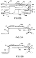
- FIGURES 12A and 12B show another method of tuning the characteristic impedance of connector 14. Specifically, it can be seen that a given spacing "C" between contact portion 24c of switch terminal 24 and the end of ground terminal 30 is greater than the spacing "D" in that area between the terminals in Figure 12B. The larger spacing "C” in Figure 12A will create a higher impedance than the smaller spacing "D” in Figure 12B. Therefore, the characteristic impedance of the connector can be tuned by adjusting this spacing between switch terminal 24 and ground terminal 30.
- FIGURES 13A and 13B show a third method of tuning the characteristic impedance of connector 14.
- Figure 13A shows a given spacing "E” between the downturned lip 34a of cross portion 34 of the U-shaped ground terminal configuration and the downturned lip 24d of the contact portion of switch terminal 24 (Fig. 3).
- Figure 13B shows a smaller spacing "F” between these downturned lips. Larger spacing "E” in Figure 13A will create a higher impedance than smaller spacing "F” between the downturned lips in Figure 13B. Therefore, the characteristic impedance of the connector can be tuned by adjusting the spacing between downturned lips 24d and 34a of switch terminal 24 and the ground terminals, respectively.
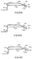
- FIGURES 14A-14C show a method of varying the size (i.e. volume) of the downturned lip 34a of cross portion 34 of the U-shaped ground terminal configuration.
- Figure 14A shows the size of the stamped and formed terminal as described above in relation to Figure 3, for instance.
- Figure 14B shows the downturned lip folded back upwardly, as at 40, to essentially double the thickness thereof. This increases the size/volume of the cross portion of the U-shaped ground terminal configuration and lowers the inductance thereof
- Figure 14C shows an alternate method wherein, rather than folding the downturned lip back upwardly, an additional strip 42 of conductive material is adhered to the outside of the downturned lip.
- the additional conductive strip 42 in Figure 14C will lower the inductance in the cross portion of the U-shaped ground terminal configuration.
- Figures 15A and 15B show a further method of tuning the impedance of connector 14.
- Figures 15A and 15B should be viewed in conjunction with Figures 5 and 10.
- Figure 15A shows overlapped area 36 corresponding to the overlapped area 36 in Figure 5, between second switch terminal 26 and second ground terminal 30.
- overlapping area 36A in Figure 10 between the second switch terminal and the second ground terminal is slightly larger than the overlapping area 36 in Figures 5 and 15A. This will result in a lower characteristic impedance because overlapping area 36A is larger than overlapping area 36.
- Figure 15B shows an overlapping area 36B which is smaller than overlapping area 36 in Figures 5 and 15A. This overlapping area 36B will result in a higher impedance because the "capacitor plate" area between the respective terminals is smaller.
Landscapes
- Details Of Connecting Devices For Male And Female Coupling (AREA)
- Coils Or Transformers For Communication (AREA)
Abstract
Description
Claims (15)
- A method of tuning the characteristic impedance of an electrical switching connector (12), comprising the steps of:providing a pair of switch terminals (24,26) having operatively engageable contact portions (24c,26c);providing a pair of ground terminals (28,30) juxtaposed alongside the switch terminals; andadjusting the spacing (A-F) between at least one of the ground terminals (28,30) and one of the switch terminals (24) to adjust the capacitance therebetween and, thereby, adjust the impedance of the connector.
- The method of claim 1 wherein the contact portion (24b,24c) of said one switch terminal (24) is elongated, and said at least one ground terminal (28,30) includes an elongated leg (28b,30b) generally parallel to the contact portion of the one switch terminal, and said adjusting step comprises adjusting the spacing (A-D) between the elongated contact portion and the elongated leg.
- The method of claim 1 wherein said pair of ground terminals (28,30) form the legs of a generally U-shaped ground terminal configuration with ends of the legs being integrally joined by a cross portion (34) of the U-shaped ground terminal configuration, and said adjusting step comprises adjusting the spacing (E,F) between the cross portion (34) and an end (24c) of one of the switch terminals (24).
- The method of claim 3, including the step of varying the size (40,42) of said cross portion (34) to adjust the inductance of the ground terminal configuration.
- The method of claim 1, including the step of overmolding a dielectric housing (14) about at least portions of said at least one ground terminal (28,30) and said one switch terminal (24) after said adjusting step.
- The method of claim 1 wherein at least a portion (26d) of one of said switch terminals (26) overlaps at least a portion of one of said ground terminals (30), and including the step of adjusting the overlapping area (36,36A,36B) to adjust the capacitance between the terminals and, thereby, adjust the impedance of the connector.
- A method of tuning the characteristic impedance of an electrical switching connector (12), comprising the steps of:providing a pair of switch terminals (24,26) having operatively engageable contact portions (24c,26c);providing a pair of ground terminals (28,30) juxtaposed alongside the switch terminals, the ground terminals forming the legs of a generally U-shaped ground terminal configuration with ends of the legs being integrally joined by a cross portion (34) of the U-shaped ground terminal configuration; andadjusting the spacing (E,F) between the cross portion (34) of the U-shaped ground terminal configuration and an end (24c) of one of the switch terminals (24).
- The method of claim 7, including the step of varying the size (40,42) of said cross portion (34) to adjust the inductance of the ground terminal configuration.
- The method of claim 7, including the step of overmolding a dielectric housing (14) about at least portions of said U-shaped ground terminal configuration and said one switch terminal (24) after said adjusting step.
- The method of claim 7 wherein at least a portion (26d) of one of said switch terminals (26) overlaps at least a portion of one of said ground terminals (30), and including the step of adjusting the overlapping area (36,36A,36B) to adjust the capacitance between the terminals and, thereby, adjust the impedance of the connector.
- A method of tuning the characteristic impedance of an electrical switching connector (12), comprising the steps of:providing a pair of switch terminals (24,26) having operatively engageable contact portions (24c,26c);providing a pair of ground terminals (28,30) juxtaposed alongside the switch terminals;overlapping at least a portion (26d) of one of the switch terminals (26) and at least a portion of one the ground terminals (30); andadjusting the overlapping area (36,36A,36B) between said overlapped terminals to adjust the capacitance between the terminals and, thereby adjust the impedance of the connector.
- The method of claim 11, including the step of overmolding a dielectric housing (14) about at least portions of at least said one ground terminal (30) after said adjusting step.
- The method of claim 12 wherein said pair of ground terminals (28,30) form the legs of a generally U-shaped ground terminal configuration with ends of the legs being integrally joined by a cross portion (34) of the U-shaped ground terminal configuration, and including the step of varying the size (40,42) of said cross portion (34) to adjust the inductance of the ground terminal configuration.
- A method of tuning the characteristic impedance of an electrical switching connector (12), comprising the steps of:providing a pair of switch terminals (24,26) having operatively engageable contact portions (24c,26c);providing a pair of ground terminals (28,30) juxtaposed alongside the switch terminals, the ground terminals forming the legs of a generally U-shaped ground terminal configuration with ends of the legs being integrally joined by a cross portion (34) of the U-shaped ground terminal configuration; andvarying the size (40,42) of said cross portion (34) to adjust the inductance of the ground terminal configuration.
- The method of claim 14, including the step of overmolding a dielectric housing (14) about at least portions of at least one ground terminal (28,30) and at least one switch terminal (24).
Applications Claiming Priority (2)
| Application Number | Priority Date | Filing Date | Title |
|---|---|---|---|
| US264947 | 1999-03-09 | ||
| US09/264,947 US6164995A (en) | 1999-03-09 | 1999-03-09 | Impedance tuning in electrical switching connector |
Publications (2)
| Publication Number | Publication Date |
|---|---|
| EP1037330A2 true EP1037330A2 (en) | 2000-09-20 |
| EP1037330A3 EP1037330A3 (en) | 2001-11-07 |
Family
ID=23008323
Family Applications (1)
| Application Number | Title | Priority Date | Filing Date |
|---|---|---|---|
| EP00105058A Withdrawn EP1037330A3 (en) | 1999-03-09 | 2000-03-09 | Impedance tuning in electrical switching connector |
Country Status (5)
| Country | Link |
|---|---|
| US (1) | US6164995A (en) |
| EP (1) | EP1037330A3 (en) |
| JP (1) | JP3381156B2 (en) |
| SG (1) | SG103254A1 (en) |
| TW (1) | TW457749B (en) |
Cited By (6)
| Publication number | Priority date | Publication date | Assignee | Title |
|---|---|---|---|---|
| WO2002082582A1 (en) * | 2001-04-09 | 2002-10-17 | Molex Incorporated | Antenna structures |
| EP1304770A3 (en) * | 2001-10-18 | 2004-02-04 | Hirose Electric Co., Ltd. | Coaxial connector with a switch |
| SG121756A1 (en) * | 2002-05-18 | 2006-05-26 | Molex Inc | Impedance tuned connector |
| EP2393167A2 (en) * | 2010-06-01 | 2011-12-07 | Hosiden Corporation | Connector |
| EP2621025B1 (en) * | 2012-01-26 | 2015-09-16 | Hosiden Corporation | Contact impedance adjusting method, contact, and connector having the same |
| EP2828934B1 (en) * | 2012-03-22 | 2018-08-01 | TE Connectivity Germany GmbH | Electrical connector having an integrated impedance equalisation element |
Families Citing this family (20)
| Publication number | Priority date | Publication date | Assignee | Title |
|---|---|---|---|---|
| DE60014385T2 (en) * | 1999-07-16 | 2006-02-23 | Molex Inc., Lisle | IMPEDANCE-CONNECTED CONNECTOR |
| US6280209B1 (en) | 1999-07-16 | 2001-08-28 | Molex Incorporated | Connector with improved performance characteristics |
| USD462053S1 (en) | 2000-11-16 | 2002-08-27 | J.S.T. Mfg. Co., Ltd. | Connector for printed circuit boards |
| USD461449S1 (en) | 2000-11-16 | 2002-08-13 | J.S.T. Mfg., Ltd. | Connector for printed circuit boards |
| USD461769S1 (en) | 2000-11-16 | 2002-08-20 | J.S.T. Mfg., Ltd. | Connector for printed circuit boards |
| US6358066B1 (en) * | 2001-02-28 | 2002-03-19 | Stratos Lightwave, Inc. | Surface mountable transceiver |
| US20030156787A1 (en) * | 2002-02-19 | 2003-08-21 | King Gregory A. | Systems and methods for aligning optical fiber to light source or detector |
| US20040092143A1 (en) * | 2002-06-11 | 2004-05-13 | Galen Fromm | High-density, impedance tuned connector |
| US7039417B2 (en) * | 2003-09-25 | 2006-05-02 | Lenovo Pte Ltd | Apparatus, system, and method for mitigating access point data rate degradation |
| WO2004001907A1 (en) * | 2002-06-21 | 2003-12-31 | Molex Incorporated | High-density, impedance-tuned connector having modular construction |
| US6863549B2 (en) * | 2002-09-25 | 2005-03-08 | Molex Incorporated | Impedance-tuned terminal contact arrangement and connectors incorporating same |
| KR100624876B1 (en) | 2004-06-21 | 2006-09-19 | 엘에스전선 주식회사 | Socket Connector with Improving Impedance Characteristics |
| JP5001740B2 (en) * | 2007-07-20 | 2012-08-15 | ホシデン株式会社 | Electrical connector |
| WO2009025868A1 (en) | 2007-08-23 | 2009-02-26 | Molex Incorporated | Board mounted electrical connector |
| JP4647675B2 (en) * | 2008-07-22 | 2011-03-09 | ホシデン株式会社 | connector |
| JP4795444B2 (en) * | 2009-02-09 | 2011-10-19 | ホシデン株式会社 | connector |
| JP5727765B2 (en) * | 2010-11-30 | 2015-06-03 | 富士通コンポーネント株式会社 | connector |
| CN103094734B (en) * | 2011-10-28 | 2016-08-10 | 富士康(昆山)电脑接插件有限公司 | Electric connector |
| JP7563322B2 (en) * | 2021-07-27 | 2024-10-08 | 株式会社オートネットワーク技術研究所 | connector |
| US20230198207A1 (en) * | 2021-12-17 | 2023-06-22 | Advanced Micro Devices, Inc. | One esd self-protect method for connector |
Family Cites Families (14)
| Publication number | Priority date | Publication date | Assignee | Title |
|---|---|---|---|---|
| US4708414A (en) * | 1987-01-30 | 1987-11-24 | Albert Lam | Electric wire connector for coaxial cable |
| US4946392A (en) * | 1988-08-09 | 1990-08-07 | Amp Incorporated | Coaxial connector in a housing block |
| JPH031460A (en) * | 1989-05-30 | 1991-01-08 | Amp Japan Ltd | Electric connector |
| JP2906469B2 (en) * | 1989-08-20 | 1999-06-21 | オムロン株式会社 | Shielded wire connector |
| JP2704305B2 (en) * | 1990-03-15 | 1998-01-26 | 日本エー・エム・ピー株式会社 | High frequency connector and method of manufacturing the same |
| MY109024A (en) * | 1992-03-24 | 1996-11-30 | Molex Inc | Impedance and inductance control in electrical connectors |
| US5522737A (en) * | 1992-03-24 | 1996-06-04 | Molex Incorporated | Impedance and inductance control in electrical connectors and including reduced crosstalk |
| US5267868A (en) * | 1992-10-01 | 1993-12-07 | Molex Incorporated | Shielded electrical connector assemblies |
| DE4236945A1 (en) * | 1992-11-02 | 1994-05-05 | Minnesota Mining & Mfg | Connection element for a high-frequency signal transmission path |
| JP3356476B2 (en) * | 1993-02-23 | 2002-12-16 | 松下電工株式会社 | TV coaxial plug |
| JPH078961U (en) * | 1993-07-14 | 1995-02-07 | 日本エー・エム・ピー株式会社 | Coaxial cable connector |
| US5304069A (en) * | 1993-07-22 | 1994-04-19 | Molex Incorporated | Grounding electrical connectors |
| NL9302115A (en) * | 1993-12-06 | 1995-07-03 | Connector Systems Tech Nv | Coax connector with impedance control. |
| US6011698A (en) * | 1996-11-12 | 2000-01-04 | Delco Electronics Corp. | Circuit protection from radio frequency energy |
-
1999
- 1999-03-09 US US09/264,947 patent/US6164995A/en not_active Expired - Fee Related
-
2000
- 2000-02-03 SG SG200000652A patent/SG103254A1/en unknown
- 2000-02-23 TW TW089103162A patent/TW457749B/en not_active IP Right Cessation
- 2000-03-03 JP JP2000058855A patent/JP3381156B2/en not_active Expired - Fee Related
- 2000-03-09 EP EP00105058A patent/EP1037330A3/en not_active Withdrawn
Cited By (8)
| Publication number | Priority date | Publication date | Assignee | Title |
|---|---|---|---|---|
| WO2002082582A1 (en) * | 2001-04-09 | 2002-10-17 | Molex Incorporated | Antenna structures |
| US6486837B2 (en) | 2001-04-09 | 2002-11-26 | Molex Incorporated | Antenna structures |
| EP1304770A3 (en) * | 2001-10-18 | 2004-02-04 | Hirose Electric Co., Ltd. | Coaxial connector with a switch |
| US6761571B2 (en) | 2001-10-18 | 2004-07-13 | Hirose Electric Co., Ltd. | Coaxial connector with a switch |
| SG121756A1 (en) * | 2002-05-18 | 2006-05-26 | Molex Inc | Impedance tuned connector |
| EP2393167A2 (en) * | 2010-06-01 | 2011-12-07 | Hosiden Corporation | Connector |
| EP2621025B1 (en) * | 2012-01-26 | 2015-09-16 | Hosiden Corporation | Contact impedance adjusting method, contact, and connector having the same |
| EP2828934B1 (en) * | 2012-03-22 | 2018-08-01 | TE Connectivity Germany GmbH | Electrical connector having an integrated impedance equalisation element |
Also Published As
| Publication number | Publication date |
|---|---|
| SG103254A1 (en) | 2004-04-29 |
| US6164995A (en) | 2000-12-26 |
| TW457749B (en) | 2001-10-01 |
| JP3381156B2 (en) | 2003-02-24 |
| EP1037330A3 (en) | 2001-11-07 |
| JP2000294346A (en) | 2000-10-20 |
Similar Documents
| Publication | Publication Date | Title |
|---|---|---|
| US6164995A (en) | Impedance tuning in electrical switching connector | |
| EP0814535B1 (en) | Surface-mount antenna and a communication apparatus using the same | |
| US5537123A (en) | Antennas and antenna units | |
| KR101413531B1 (en) | Electric connector | |
| US6751317B2 (en) | Movable terminal, coaxial connector, and communication apparatus incorporating the same | |
| US6392603B1 (en) | Module antenna device | |
| US6142804A (en) | Electrical switching connector | |
| JPH0653733A (en) | Resonator antenna | |
| NL9302115A (en) | Coax connector with impedance control. | |
| EP0545289A1 (en) | Coaxial microstrip line transducer | |
| US5668557A (en) | Surface-mount antenna and communication device using same | |
| US5278527A (en) | Dielectric filter and shield therefor | |
| EP0707355A1 (en) | Antenna device | |
| EP0940877A1 (en) | Nonreciprocal circuit device | |
| EP1821368A1 (en) | Connector between substrates, and circuit board device using connector between substrates | |
| EP1067621A2 (en) | Nonreciprocal device and communication device using the same | |
| CN217427092U (en) | Antenna coupling electric conductor and radio frequency device | |
| US11909097B2 (en) | Monolithic antenna integrated radio frequency connector | |
| US20060232481A1 (en) | Wideband antenna module for the high-frequency and microwave range | |
| WO1999022418A1 (en) | Matching device for a multi-frequency antenna | |
| KR100734917B1 (en) | DW-H antenna for mobile communication terminal | |
| EP1146588A2 (en) | Snap-fit antenna for portable communications devices | |
| WO2003073556A1 (en) | Low profile antenna and interconnect | |
| JPH0676888A (en) | Coaxial connector | |
| CN118040319A (en) | Antenna assembly for 5G mobile terminal |
Legal Events
| Date | Code | Title | Description |
|---|---|---|---|
| PUAI | Public reference made under article 153(3) epc to a published international application that has entered the european phase |
Free format text: ORIGINAL CODE: 0009012 |
|
| AK | Designated contracting states |
Kind code of ref document: A2 Designated state(s): AT BE CH CY DE DK ES FI FR GB GR IE IT LI LU MC NL PT SE Kind code of ref document: A2 Designated state(s): DE FR GB IT |
|
| AX | Request for extension of the european patent |
Free format text: AL;LT;LV;MK;RO;SI |
|
| PUAL | Search report despatched |
Free format text: ORIGINAL CODE: 0009013 |
|
| AK | Designated contracting states |
Kind code of ref document: A3 Designated state(s): AT BE CH CY DE DK ES FI FR GB GR IE IT LI LU MC NL PT SE |
|
| AX | Request for extension of the european patent |
Free format text: AL;LT;LV;MK;RO;SI |
|
| 17P | Request for examination filed |
Effective date: 20020427 |
|
| AKX | Designation fees paid |
Free format text: DE FR GB IT |
|
| STAA | Information on the status of an ep patent application or granted ep patent |
Free format text: STATUS: THE APPLICATION IS DEEMED TO BE WITHDRAWN |
|
| 18D | Application deemed to be withdrawn |
Effective date: 20031001 |