EP1037281A1 - Capacitor trench-top dielectric for self-aligned device isolation - Google Patents
Capacitor trench-top dielectric for self-aligned device isolation Download PDFInfo
- Publication number
- EP1037281A1 EP1037281A1 EP00103964A EP00103964A EP1037281A1 EP 1037281 A1 EP1037281 A1 EP 1037281A1 EP 00103964 A EP00103964 A EP 00103964A EP 00103964 A EP00103964 A EP 00103964A EP 1037281 A1 EP1037281 A1 EP 1037281A1
- Authority
- EP
- European Patent Office
- Prior art keywords
- trench
- trenches
- deep
- substrate
- dielectric layer
- Prior art date
- Legal status (The legal status is an assumption and is not a legal conclusion. Google has not performed a legal analysis and makes no representation as to the accuracy of the status listed.)
- Granted
Links
Images


Classifications
-
- H—ELECTRICITY
- H10—SEMICONDUCTOR DEVICES; ELECTRIC SOLID-STATE DEVICES NOT OTHERWISE PROVIDED FOR
- H10B—ELECTRONIC MEMORY DEVICES
- H10B12/00—Dynamic random access memory [DRAM] devices
- H10B12/01—Manufacture or treatment
- H10B12/02—Manufacture or treatment for one transistor one-capacitor [1T-1C] memory cells
- H10B12/03—Making the capacitor or connections thereto
- H10B12/038—Making the capacitor or connections thereto the capacitor being in a trench in the substrate
- H10B12/0385—Making a connection between the transistor and the capacitor, e.g. buried strap
-
- H—ELECTRICITY
- H10—SEMICONDUCTOR DEVICES; ELECTRIC SOLID-STATE DEVICES NOT OTHERWISE PROVIDED FOR
- H10W—GENERIC PACKAGES, INTERCONNECTIONS, CONNECTORS OR OTHER CONSTRUCTIONAL DETAILS OF DEVICES COVERED BY CLASS H10
- H10W10/00—Isolation regions in semiconductor bodies between components of integrated devices
-
- H—ELECTRICITY
- H10—SEMICONDUCTOR DEVICES; ELECTRIC SOLID-STATE DEVICES NOT OTHERWISE PROVIDED FOR
- H10W—GENERIC PACKAGES, INTERCONNECTIONS, CONNECTORS OR OTHER CONSTRUCTIONAL DETAILS OF DEVICES COVERED BY CLASS H10
- H10W10/00—Isolation regions in semiconductor bodies between components of integrated devices
- H10W10/01—Manufacture or treatment
-
- H—ELECTRICITY
- H10—SEMICONDUCTOR DEVICES; ELECTRIC SOLID-STATE DEVICES NOT OTHERWISE PROVIDED FOR
- H10B—ELECTRONIC MEMORY DEVICES
- H10B12/00—Dynamic random access memory [DRAM] devices
- H10B12/01—Manufacture or treatment
- H10B12/02—Manufacture or treatment for one transistor one-capacitor [1T-1C] memory cells
- H10B12/03—Making the capacitor or connections thereto
- H10B12/038—Making the capacitor or connections thereto the capacitor being in a trench in the substrate
- H10B12/0383—Making the capacitor or connections thereto the capacitor being in a trench in the substrate wherein the transistor is vertical
Definitions
- the invention relates to semiconductor devices.
- the present invention relates to dynamic random access memory (DRAM) devices.
- DRAM dynamic random access memory
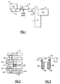
- a merged isolation node trench (MINT) cell is illustrated in Fig. 1.
- the MINT cell illustrated in Fig. 1 includes a planar transfer device.
- the device shown in Fig. 1 includes a deep trench capacitor 1 a shallow trench isolation region 2 used to define the active area, a bit line contact (CB) 3, a word line (WL) 5, or transfer device gate, gate oxide 7 and N+ source/drain regions 9 and 11.
- a buried strap 12 connects the deep trench capacitor storage trench node 1 to the source/drain diffusion 11 of the transfer device.
- MINT buried strap resistance may be a function of the overlap of the deep trench 1 and the shallow trench isolation region 2 of the memory cell.
- the invention addresses MINT buried strap resistance as a function of overlay between the deep trench and active area overlay making the shallow trench isolation pattern self-aligned to the deep trench to ensure full trench width for buried strap formation.
- the present invention provides a semiconductor device including a substrate. At least one pair of deep trenches is arranged in the substrate. A collar lines at least a portion of a wall of each deep trench. The trenches contain a conductive fill material. A buried strap extends completely across each trench over each trench fill and each collar. An isolation region is arranged between the deep trenches. A dielectric region overlies each buried strap in each deep trench.
- aspects of the present invention also provide a process for forming an active area and shallow trench isolation self-aligned to a deep trench.
- the process includes forming at least one pair of adjacent deep trenches in a substrate and through a first dielectric layer on a surface of the substrate.
- a dielectric collar is provided on at least a portion of a side wall of each deep trench.
- the deep trenches are filled.
- a top surface of the deep trench fill is recessed.
- a portion of the deep trench collars is etched.
- a strap material is deposited on the deep trench fill and within the recessed deep trench collars.
- a second dielectric layer is deposited on exposed surfaces of the strap material, the substrate, and the first dielectric layer.
- the structure is planarized, thereby removing portions of the second dielectric layer, such that the second dielectric layer only remains in the deep trenches.
- a layer of photoresist is deposited. The photoresist is patterned to expose portions of the second dielectric layer in the deep trenches and portions of the first dielectric layer such that at least a portion of the photoresist remains overlapping the deep trench. Portions of the first dielectric layer between the trenches are selectively removed. A portion of the second dielectric layer in the trenches and a portion of the substrate between the trenches are selectively removed.
- a third dielectric layer is deposited in spaces created by removal of the portions of the first dielectric layer and portions of the second dielectric layer. The third dielectric layer is then planarized. Remaining portions of the first dielectric layer are removed.
- the deep trench and active area pattern may be misaligned.
- buried strap resistance is a function of deep trench-active area overlay. Therefore, misalignment of the deep trench-active area overlay may alter buried strap resistance, and cause an increase in the variation of the series resistance of the buried strap due to the manufacturing tolerance of the misalignment.
- Fig. 2 illustrates an overhead view of a portion of a semiconductor device structure showing a plurality of deep trenches and illustrating deep trench-active area overlay.
- Fig. 2 illustrates deep trenches 14, gate conductors 16, active areas 18 and diffusion contact (CB) regions 20.
- Fig. 2 also illustrates two examples of deep trench-active area overlay.
- Deep trench-active area overlay area 22 illustrates a more favorable amount of overlay between the active area and the deep trench. On the other hand, deep trench-active area region 24 is less desirable.
- Fig. 3 illustrates a cross-sectional view of an example of less favorable deep trench-active area overlay 32.
- Fig. 3 illustrates filled deep trenches 26 each having an associated collar region 28.
- Shallow trench isolation region 30 overlies deep trenches 26 as well as a region between the deep trenches.
- the present invention provides a solution for ensuring favorable deep trench-active area overlay by providing a process for making the active area pattern self-aligned to the deep trench to ensure the full trench width for buried strap formation.
- Processes according to the present invention would be utilized to form a MINT-based deep trench capacitor and shallow trench isolation region using a trench top oxide region as a masking layer for the shallow trench isolation region.
- Processes according to the present invention may also be utilized for forming other semiconductor devices.
- a substrate 34 may be provided.
- a dielectric layer 36 may be provided on the top surface of the substrate.
- the dielectric layer is a nitride.
- nitride that may be utilized as the dielectric layer 36 is silicon nitride SiN.
- additional thin dielectric layers, such as silicon dioxide, may be included in the dielectric layer 36.
- deep trenches 38 may be formed through dielectric layer 36 into substrate 34 using standard lithographic and dry etch techniques, such as reactive ion etching (RIE).
- RIE reactive ion etching
- a collar 40 may be formed on a portion of the surface 42 of each deep trench 38.
- the collar may be formed of a dielectric material, such as silicon dioxide.
- the collar may be formed by oxidation of the trench wall.
- the collar is formed in an upper region of each deep trench 38 such that the collar, when formed, extends all of the way to the top of the deep trenches 38.
- the substrate material forming the walls 42 of deep trenches 38 may be oxidized to form the collar 40.
- the deep trenches are filled with a conductive material.
- Fig. 6 illustrates an example of filled deep trenches.
- the deep trenches may first be filled with a desired material. Examples of materials that may be utilized to fill the deep trenches include various semiconductor materials. For example, polycrystalline silicon may be utilized as a deep trench fill.
- the upper surface of the structure illustrated in Fig. 6 may be planarized to remove any deep trench fill that may have been deposited the upper surface of the structure.
- the deep trench fill may then be recessed below the opening of the deep trench at the upper level of the substrate.
- the recessing may be carried out utilizing a dry etch technique, such as RIE.
- the deep trench fill may be recessed below the interface of substrate 34 and dielectric layer 36.
- Fig. 6 illustrates recessed deep trench fill 44.
- the collars 40 may be isotropically etched away from the exposed sidewalls of the trenches such that the top surface of the collars is below the top surface of the trench fill. Etching of the collars 40 may be carried out with a wet etch process.
- Fig. 7 illustrates recessed collar structures 40.
- a buried strap may be formed in each deep trench.
- the deep strap may be formed so as to extend entirely across the deep trenches.
- the buried straps may be formed of a semiconductor material.
- the buried straps may be formed of silicon.
- any suitable technique may be utilized for forming the buried strap.
- chemical vapor deposition may be utilized.
- low pressure chemical vapor deposition LCVD
- LCVD low pressure chemical vapor deposition
- the buried strap may be formed so as to cover the trench fill 44 as well as the collar structures 40.
- the material may be recessed.
- Fig. 8 illustrates an example of buried straps 46 formed over the trench fill 44 and recessed collar 40 after the strap silicon has been isotropically removed from the wafer surface and trench sidewalls.
- a liner 48 may be formed over dielectric layer 36, surfaces of the dielectric layer 36 lining the opening above the deep trenches, the walls of the deep trenches above the strap 46, and the surface of the straps although this is not shown in the Figures. It is not necessary that the present invention include a liner. Rather, the liner is an optional structure.
- the liner may be formed of a dielectric material. According to one example, the liner is formed of an LPCVD nitride having a thickness of about 2 nm to about 10 nm.
- One particular nitride that may be utilized in the liner is silicon nitride SiN.
- a dielectric material 50 may be deposited over the liner. If the present invention does not include a liner, then the dielectric layer would be deposited over the same structures described above that the liner would be deposited on. Any suitable dielectric may be utilized. According to one example, an oxide may be utilized to form dielectric layer 50. One example of an oxide that may be utilized is silicon dioxide.
- Fig. 9 illustrates a structure including the liner 48 and dielectric region 50.
- portions of dielectric 50 lying above dielectric region 36 may be removed by planarizing, such as by chemical mechanical polishing (CMP), the dielectric region 50.
- CMP chemical mechanical polishing
- regions of the liner lying on top of the dielectric region 36 may also be removed, if the structure includes a liner.
- Fig. 10 illustrates the structure resulting from planarization of the dielectric region 50. As can be seen in Fig. 10, the remaining portions of dielectric region 50 lie within the deep trench and within the opening in the dielectric region 36 lying above the deep trenches. These dielectric regions 52 may form a trench top region at the top of each deep trench. In the event that dielectric material 50 was an oxide, regions 52 may be referred to as a trench top oxide (TTO).
- TTO trench top oxide
- photoresist 54 may be deposited over the entire upper surface of the structure. After depositing the photoresist, the photoresist may be patterned to form an active area and shallow trench isolation pattern on the structure.
- Fig. 11 illustrates an example of pattern photoresist 54 on a structure. The photoresist illustrated in Fig. 11 has been patterned to expose a portion of each trench top region 52 as well as a region of dielectric 36 between the deep trenches. Traditional photolithography processes may be utilized to pattern the photoresist to form the mask.
- the regions of the structure exposed by removal of portions of the photoresist may be etched.
- a reactive ion etch is utilized.
- the etch may includes fluorine, carbon and oxygen feed gas. Examples of such gasses can include CF 4 , CHF 3 , Ar, O 2 , CO, C 2 F 6 , C 4 F 6 , and/or C 3 F 8 .
- the etch process may be carried out in a plurality of steps. For example, a first etch may be utilized to etch only the portions of dielectric region 36 but not portions of dielectric 52. Such an etch may be considered to etch the dielectric 36 selective to dielectric 52. At least a portion of the substrate underlying regions of dielectric layer 36 may be removed by the etch. This etch may also be considered to be selective to the photoresist.
- Fig. 12 illustrates a region 56 adjacent the deep trenches created by the etch.
- the resulting structures may now be considered to represent to portions of a semiconductor device divided by line 58. These portions are the array 60 and the supporting structure 62.
- the region 56 created by the etch represents a part of the supporting structures.
- the support structures may include conventional transistors and shallow trench isolation regions.
- a second etch may now carried out to etch the silicon substrate.
- This second etch will be selective to the exposed portions of the trench top structures 52.
- the substrate may be etched down to a level that lies below the strap structure 46 and below the top of the collar regions 40.
- the region between the deep trenches as well as the support structure opening 56 may be etched to the same level. Alternatively, these two regions may be etched to differential levels.
- at least a portion of the trench top regions 52 may also be etched.
- This second etch may be considered to be an etch of the silicon selective to the dielectric 52 as well as photoresist 54 and can be dry etch using feed gases, such as Cl 2 , HCl, HBr, and/or BCl 3 .
- region 64 may form an isolation region, typically a shallow isolation region, between the deep trenches. Material filling isolation region 64 may also be utilized to fill support structure trench 56. The regions 56 and 64 may be filled simultaneously.
- the material deposited in region 64 may be a dielectric material.
- the dielectric material deposited in region 64 is an oxide, such as silicon oxide.
- the dielectric material forms a shallow trench isolation region.
- the upper surface of the structure may be planarized to remove regions of dielectric material lying outside of the space forming the isolation region. The planarization may be carried out using CMP.
- dielectric region 36 may be removed from the upper surface of the substrate. Planarization of dielectric material filling the isolation region 64 may also remove portions of the trench top regions 52 as well as dielectric region 36. This planarization step may be useful to result in co-planar top surfaces of the trench top regions 52 and isolation regions 64. The planarization step may also help to make the top of the support structure 56 co-planar with the trench top regions 52 and isolation region 64.
- Fig. 14 illustrates an embodiment of the device structure at this stage in the process.
- transistor and other devices may then be formed over at least one of the deep trenches and over the support structure.
- the device structures formed over the structure illustrated in Fig. 15 may include gate conductor regions. Middle of line regions including contacts to diffusion regions and to the gate conductor and the first level of interconnect wiring, typically known as metal 0 (M0) may also be formed over the deep trenches and/or supporting structure using standard processing techniques.
- M0 metal 0
- the present invention also provides a process for forming an active area in shallow trench isolation self-aligned to a deep trench.
- the process includes providing a substrate having a layer of nitride on the surface. At least one pair of adjacent deep trenches is formed through the nitride and in the substrate.
- An oxide collar is provided on at least a portion of a sidewall of each trench.
- the trenches are filled with polycrystalline silicon.
- a top surface of the trench fill is recessed.
- a portion of the trench collars is etched.
- An oxide strap material is deposited on the trench fill and over the recessed trench collars.
- a liner may be deposited on exposed surfaces of the strap material, the substrate, and the nitride layer on the substrate.
- An oxide layer is deposited on the liner or on the structures that the liner is deposited on if the invention does not include a liner. The entire structure is planarized to remove portions of the oxide layer on the liner and portions of the liner, such that the oxide layer only remains in the trenches. If the structure does not include a liner, then only portions of the oxide layer would be removed.
- Photoresist is deposited over the structure.
- the photoresist is patterned to expose portions of the oxide layer in the trenches and the nitride layer on the substrate such that at least a portion of the photoresist remains overlapping the deep trench.
- Portions of the nitride layer on the substrate between the trenches are selectively removed.
- a portion of the oxide layer in the trenches and a portion of the substrate between the trenches are selectively removed.
- An oxide is deposited in spaces created by removal of the nitride layer on a substrate between the trenches and in the portions of the oxide layer in the trenches.
- the oxide is then planarized. Nitride remaining on the surface of the substrate is removed.
- Transistor devices are formed over at least one of the deep trenches.
- the present invention also includes a semiconductor device formed by a process as described above.
- a semiconductor device according to the present invention may be formed according to the above described processes. Alternatively, other processes may be utilized to form a semiconductor device according to the present invention.
- a semiconductor device includes a substrate. At least one pair of deep trenches is arranged in the substrate. The deep trenches may be parallel or substantially parallel as described above. A trench fill may be arranged in each deep trench. An isolation region may be arranged between the trenches.
- the present invention may include a plurality of pairs of deep trenches. Each pair being as described above.
- a buried plate structure may be arranged in each substrate in association with each pair of deep trenches.
- a collar region lines at least a portion of a wall of each deep trench.
- the collar may be arranged in each deep trench in the vicinity of an upper portion of each deep trench.
- the collar may be formed of a dielectric material.
- the dielectric material may be an oxide.
- One example of an dielectric material that may be utilized is silicon dioxide SiO 2 .
- a buried strap extending completely across each deep trench over each deep trench fill and each collar.
- a dielectric region may overlay each buried strap in each deep trench.
- a liner may be arranged between each strap and each dielectric region.
- Transistor devices and interconnection structures may be formed above at least one of the deep trenches.
- a support structure may be formed in the substrate remote from deep trenches.
- the support structure isolation trenches may be filled with a dielectric material.
- the dielectric material may be an oxide.
- One example of an oxide that may be utilized is silicon dioxide SiO 2 .
- the array region is shown as region 60, and the support structures are shown as region 61 in Fig. 15.
- the materials comprising each region of a semiconductor device according to the present invention may be as described above in relation to a process of the present invention.
- the advantages of the present invention are that it is not necessary to rely on critical alignment of the AA pattern level to the deep trench pattern level. As long as part of the AA pattern overlaps the deep trench, this may provide a strap. Additionally, according to the present invention, the deep trench may be made smaller in diameter because the critical overlap tolerance between the AA level and deep trench level is increased.
- the present invention a greater amount of misalignment can be tolerated than according to prior methods and structures because the active area photoresist pattern need only cover the edge of the trench top structure over the deep trench in order to ensure that there is a good conduction path from the active area through the strap and into the deep trench storage capacitor.
- the shallow trench isolation may only lie between back-to-back trenches and as such will not cut into strap width as in DRAM cells, such as those illustrated in Figs. 2 and 3.
- the present invention may also help to eliminate the active area-deep trench overlay sensitivity of the buried strap resistance by merging the active area and deep trench patterns.
Landscapes
- Engineering & Computer Science (AREA)
- Manufacturing & Machinery (AREA)
- Semiconductor Memories (AREA)
- Element Separation (AREA)
Abstract
Description
- This application is related to U.S. patent application serial number 09/233,887, for Improved Process For Buried Strap Self-Aligned To Deep Storage Trench, tiled January 20, 1999, the entire contents of the disclosure of which is hereby incorporated by reference.
- The invention relates to semiconductor devices. In particular, the present invention relates to dynamic random access memory (DRAM) devices.
- Increasing numbers of semiconductor devices, such as individual memory cells, are being created on a single chip. As a result, dimensions of the devices continue to shrink. Shrinking device dimensions can increase the difficulty of ensuring proper alignment over an adequate functional area of the structures included in the semiconductor devices.
- For example, a merged isolation node trench (MINT) cell is illustrated in Fig. 1. The MINT cell illustrated in Fig. 1 includes a planar transfer device. The device shown in Fig. 1 includes a deep trench capacitor 1 a shallow
trench isolation region 2 used to define the active area, a bit line contact (CB) 3, a word line (WL) 5, or transfer device gate, gate oxide 7 and N+ source/drain regions 9 and 11. In the structure illustrated in Fig. 1, a buriedstrap 12 connects the deep trench capacitorstorage trench node 1 to the source/drain diffusion 11 of the transfer device. In a MINT cell, MINT buried strap resistance may be a function of the overlap of thedeep trench 1 and the shallowtrench isolation region 2 of the memory cell. - The invention addresses MINT buried strap resistance as a function of overlay between the deep trench and active area overlay making the shallow trench isolation pattern self-aligned to the deep trench to ensure full trench width for buried strap formation.
- In accordance with these and other objects and advantages, the present invention provides a semiconductor device including a substrate. At least one pair of deep trenches is arranged in the substrate. A collar lines at least a portion of a wall of each deep trench. The trenches contain a conductive fill material. A buried strap extends completely across each trench over each trench fill and each collar. An isolation region is arranged between the deep trenches. A dielectric region overlies each buried strap in each deep trench.
- Aspects of the present invention also provide a process for forming an active area and shallow trench isolation self-aligned to a deep trench. The process includes forming at least one pair of adjacent deep trenches in a substrate and through a first dielectric layer on a surface of the substrate. A dielectric collar is provided on at least a portion of a side wall of each deep trench. The deep trenches are filled. A top surface of the deep trench fill is recessed. A portion of the deep trench collars is etched. A strap material is deposited on the deep trench fill and within the recessed deep trench collars. A second dielectric layer is deposited on exposed surfaces of the strap material, the substrate, and the first dielectric layer. The structure is planarized, thereby removing portions of the second dielectric layer, such that the second dielectric layer only remains in the deep trenches. A layer of photoresist is deposited. The photoresist is patterned to expose portions of the second dielectric layer in the deep trenches and portions of the first dielectric layer such that at least a portion of the photoresist remains overlapping the deep trench. Portions of the first dielectric layer between the trenches are selectively removed. A portion of the second dielectric layer in the trenches and a portion of the substrate between the trenches are selectively removed. A third dielectric layer is deposited in spaces created by removal of the portions of the first dielectric layer and portions of the second dielectric layer. The third dielectric layer is then planarized. Remaining portions of the first dielectric layer are removed.
- Further aspects of the present invention provide a semiconductor device formed by the above process.
- Still other objects and advantages of the present invention will become readily apparent by those skilled in the art from the following detailed description, wherein it is shown and described only the preferred embodiments of the invention, simply by way of illustration of the best mode contemplated of carrying out the invention. As will be realized, the invention is capable of other and different embodiments, and its several details are capable of modifications in various obvious respects, without departing from the invention. Accordingly, the drawings and description are to be regarded as illustrative in nature and not as restrictive.
- The above-mentioned objects and advantages of the present invention will be more clearly understood when considered in conjunction with the accompanying drawings, in which:
- Fig. 1 represents a cross-sectional view of an example of a known DRAM cell structure;
- Fig. 2 represents an overhead view of an embodiment of a DRAM cell structure illustrating examples of more desirable and less desirable overlaps of deep trenches and active areas;
- Fig. 3 represents a cross-sectional view of a less desirable deep trench to active area overlay; and
- Figs. 4-15 represent cross-sectional views of an embodiment of a semiconductor device structure according to the present invention at various stages of an embodiment of a process according to the present invention.
-
- As semiconductor device dimensions decrease and an increasing number of devices are packed into one space, problems may arise as a result of device crowding and aligning devices and portions of devices with ever decreasing dimensions. For example, in some memory cells, the deep trench and active area pattern may be misaligned. One problem resulting from this is that buried strap resistance is a function of deep trench-active area overlay. Therefore, misalignment of the deep trench-active area overlay may alter buried strap resistance, and cause an increase in the variation of the series resistance of the buried strap due to the manufacturing tolerance of the misalignment.
- Fig. 2 illustrates an overhead view of a portion of a semiconductor device structure showing a plurality of deep trenches and illustrating deep trench-active area overlay. Fig. 2 illustrates
deep trenches 14,gate conductors 16,active areas 18 and diffusion contact (CB)regions 20. Fig. 2 also illustrates two examples of deep trench-active area overlay. Deep trench-activearea overlay area 22 illustrates a more favorable amount of overlay between the active area and the deep trench. On the other hand, deep trench-active area region 24 is less desirable. - Fig. 3 illustrates a cross-sectional view of an example of less favorable deep trench-
active area overlay 32. Fig. 3 illustrates filleddeep trenches 26 each having an associatedcollar region 28. Shallowtrench isolation region 30 overliesdeep trenches 26 as well as a region between the deep trenches. - The present invention provides a solution for ensuring favorable deep trench-active area overlay by providing a process for making the active area pattern self-aligned to the deep trench to ensure the full trench width for buried strap formation. Processes according to the present invention would be utilized to form a MINT-based deep trench capacitor and shallow trench isolation region using a trench top oxide region as a masking layer for the shallow trench isolation region. Processes according to the present invention may also be utilized for forming other semiconductor devices.
- According to the structure of the present invention illustrated in Figs. 4-15, a
substrate 34 may be provided. Adielectric layer 36 may be provided on the top surface of the substrate. According to one example, the dielectric layer is a nitride. In particular, nitride that may be utilized as thedielectric layer 36 is silicon nitride SiN. Although not shown in the figures, additional thin dielectric layers, such as silicon dioxide, may be included in thedielectric layer 36. After providing asubstrate 34 withdielectric layer 36 arranged on the top surface thereof,deep trenches 38 may be formed throughdielectric layer 36 intosubstrate 34 using standard lithographic and dry etch techniques, such as reactive ion etching (RIE). - After formation of
deep trenches 38, acollar 40 may be formed on a portion of thesurface 42 of eachdeep trench 38. The collar may be formed of a dielectric material, such as silicon dioxide. - The collar may be formed by oxidation of the trench wall. Typically, the collar is formed in an upper region of each
deep trench 38 such that the collar, when formed, extends all of the way to the top of thedeep trenches 38. In other words, the substrate material forming thewalls 42 ofdeep trenches 38 may be oxidized to form thecollar 40. - After formation of the
collar regions 40, the deep trenches are filled with a conductive material. Fig. 6 illustrates an example of filled deep trenches. The deep trenches may first be filled with a desired material. Examples of materials that may be utilized to fill the deep trenches include various semiconductor materials. For example, polycrystalline silicon may be utilized as a deep trench fill. - After filling the deep trenches, the upper surface of the structure illustrated in Fig. 6 may be planarized to remove any deep trench fill that may have been deposited the upper surface of the structure. The deep trench fill may then be recessed below the opening of the deep trench at the upper level of the substrate. The recessing may be carried out utilizing a dry etch technique, such as RIE. In other words, the deep trench fill may be recessed below the interface of
substrate 34 anddielectric layer 36. Fig. 6 illustrates recessed deep trench fill 44. - After filling the deep trenches and recessing the trench fill to a desired level, the
collars 40 may be isotropically etched away from the exposed sidewalls of the trenches such that the top surface of the collars is below the top surface of the trench fill. Etching of thecollars 40 may be carried out with a wet etch process. Fig. 7 illustrates recessedcollar structures 40. - After recessing the
collar structures 40, a buried strap may be formed in each deep trench. According to the present invention, the deep strap may be formed so as to extend entirely across the deep trenches. The buried straps may be formed of a semiconductor material. According to one embodiment, the buried straps may be formed of silicon. - Any suitable technique may be utilized for forming the buried strap. For example, chemical vapor deposition may be utilized. According to one embodiment, low pressure chemical vapor deposition (LP CVD) may be utilized to form the buried strap.
- The buried strap may be formed so as to cover the trench fill 44 as well as the
collar structures 40. In one embodiment of the invention, after depositing the buried strap material, the material may be recessed. Fig. 8 illustrates an example of buriedstraps 46 formed over the trench fill 44 and recessedcollar 40 after the strap silicon has been isotropically removed from the wafer surface and trench sidewalls. - After formation of the buried
strap structures 46, aliner 48 may be formed overdielectric layer 36, surfaces of thedielectric layer 36 lining the opening above the deep trenches, the walls of the deep trenches above thestrap 46, and the surface of the straps although this is not shown in the Figures. It is not necessary that the present invention include a liner. Rather, the liner is an optional structure. The liner may be formed of a dielectric material. According to one example, the liner is formed of an LPCVD nitride having a thickness of about 2 nm to about 10 nm. One particular nitride that may be utilized in the liner is silicon nitride SiN. In addition, it may be desired to form a thin thermal oxidation of about 2 nm to about 10 nm prior to deposition of the liner. - After formation of the
liner structure 48, adielectric material 50 may be deposited over the liner. If the present invention does not include a liner, then the dielectric layer would be deposited over the same structures described above that the liner would be deposited on. Any suitable dielectric may be utilized. According to one example, an oxide may be utilized to formdielectric layer 50. One example of an oxide that may be utilized is silicon dioxide. - Fig. 9 illustrates a structure including the
liner 48 anddielectric region 50. - After deposition of
dielectric layer 50, portions of dielectric 50 lying abovedielectric region 36 may be removed by planarizing, such as by chemical mechanical polishing (CMP), thedielectric region 50. During this planarization step, regions of the liner lying on top of thedielectric region 36 may also be removed, if the structure includes a liner. Fig. 10 illustrates the structure resulting from planarization of thedielectric region 50. As can be seen in Fig. 10, the remaining portions ofdielectric region 50 lie within the deep trench and within the opening in thedielectric region 36 lying above the deep trenches. Thesedielectric regions 52 may form a trench top region at the top of each deep trench. In the event thatdielectric material 50 was an oxide,regions 52 may be referred to as a trench top oxide (TTO). - After removing portions of the
dielectric region 50 to create trenchtop regions 52,photoresist 54 may be deposited over the entire upper surface of the structure. After depositing the photoresist, the photoresist may be patterned to form an active area and shallow trench isolation pattern on the structure. Fig. 11 illustrates an example ofpattern photoresist 54 on a structure. The photoresist illustrated in Fig. 11 has been patterned to expose a portion of eachtrench top region 52 as well as a region of dielectric 36 between the deep trenches. Traditional photolithography processes may be utilized to pattern the photoresist to form the mask. - After formation of desired
mask pattern 54 over the deep trench and other underlying structures, the regions of the structure exposed by removal of portions of the photoresist may be etched. Typically, a reactive ion etch is utilized. The etch may includes fluorine, carbon and oxygen feed gas. Examples of such gasses can include CF4, CHF3, Ar, O2, CO, C2F6, C4F6, and/or C3F8. - The etch process may be carried out in a plurality of steps. For example, a first etch may be utilized to etch only the portions of
dielectric region 36 but not portions ofdielectric 52. Such an etch may be considered to etch the dielectric 36 selective to dielectric 52. At least a portion of the substrate underlying regions ofdielectric layer 36 may be removed by the etch. This etch may also be considered to be selective to the photoresist. Fig. 12 illustrates aregion 56 adjacent the deep trenches created by the etch. - The resulting structures may now be considered to represent to portions of a semiconductor device divided by
line 58. These portions are thearray 60 and the supportingstructure 62. Theregion 56 created by the etch represents a part of the supporting structures. The support structures may include conventional transistors and shallow trench isolation regions. - A second etch may now carried out to etch the silicon substrate. This second etch will be selective to the exposed portions of the
trench top structures 52. As illustrated in Fig. 13, the substrate may be etched down to a level that lies below thestrap structure 46 and below the top of thecollar regions 40. The region between the deep trenches as well as thesupport structure opening 56 may be etched to the same level. Alternatively, these two regions may be etched to differential levels. As illustrated in Fig. 13, during the etching of the substrate, at least a portion of thetrench top regions 52 may also be etched. This second etch may be considered to be an etch of the silicon selective to the dielectric 52 as well asphotoresist 54 and can be dry etch using feed gases, such as Cl2, HCl, HBr, and/or BCl3. - After etching of the
dielectric region 36, substrate, and trenchtop regions 52, remainingphotoresist 54 may be removed from the upper surface of the structure. Also after etching the dielectric 36, substrate and trench top regions, material may be deposited inregion 64.Region 64 may form an isolation region, typically a shallow isolation region, between the deep trenches. Material fillingisolation region 64 may also be utilized to fillsupport structure trench 56. Theregions - The material deposited in
region 64 may be a dielectric material. According to one example, the dielectric material deposited inregion 64 is an oxide, such as silicon oxide. The dielectric material forms a shallow trench isolation region. After depositing the dielectric to formregion 64, the upper surface of the structure may be planarized to remove regions of dielectric material lying outside of the space forming the isolation region. The planarization may be carried out using CMP. - After filling
isolation region 64,dielectric region 36 may be removed from the upper surface of the substrate. Planarization of dielectric material filling theisolation region 64 may also remove portions of thetrench top regions 52 as well asdielectric region 36. This planarization step may be useful to result in co-planar top surfaces of thetrench top regions 52 andisolation regions 64. The planarization step may also help to make the top of thesupport structure 56 co-planar with thetrench top regions 52 andisolation region 64. Fig. 14 illustrates an embodiment of the device structure at this stage in the process. - After formation of the structure shown in Fig. 14, transistor and other devices may then be formed over at least one of the deep trenches and over the support structure. The device structures formed over the structure illustrated in Fig. 15 may include gate conductor regions. Middle of line regions including contacts to diffusion regions and to the gate conductor and the first level of interconnect wiring, typically known as metal 0 (M0) may also be formed over the deep trenches and/or supporting structure using standard processing techniques.
- According to one particular embodiment, the present invention also provides a process for forming an active area in shallow trench isolation self-aligned to a deep trench. The process includes providing a substrate having a layer of nitride on the surface. At least one pair of adjacent deep trenches is formed through the nitride and in the substrate.
- An oxide collar is provided on at least a portion of a sidewall of each trench. The trenches are filled with polycrystalline silicon. A top surface of the trench fill is recessed. A portion of the trench collars is etched. An oxide strap material is deposited on the trench fill and over the recessed trench collars. A liner may be deposited on exposed surfaces of the strap material, the substrate, and the nitride layer on the substrate. An oxide layer is deposited on the liner or on the structures that the liner is deposited on if the invention does not include a liner. The entire structure is planarized to remove portions of the oxide layer on the liner and portions of the liner, such that the oxide layer only remains in the trenches. If the structure does not include a liner, then only portions of the oxide layer would be removed.
- Photoresist is deposited over the structure. The photoresist is patterned to expose portions of the oxide layer in the trenches and the nitride layer on the substrate such that at least a portion of the photoresist remains overlapping the deep trench. Portions of the nitride layer on the substrate between the trenches are selectively removed. A portion of the oxide layer in the trenches and a portion of the substrate between the trenches are selectively removed. An oxide is deposited in spaces created by removal of the nitride layer on a substrate between the trenches and in the portions of the oxide layer in the trenches. The oxide is then planarized. Nitride remaining on the surface of the substrate is removed. Transistor devices are formed over at least one of the deep trenches.
- The present invention also includes a semiconductor device formed by a process as described above. A semiconductor device according to the present invention may be formed according to the above described processes. Alternatively, other processes may be utilized to form a semiconductor device according to the present invention.
- A semiconductor device according to the present invention includes a substrate. At least one pair of deep trenches is arranged in the substrate. The deep trenches may be parallel or substantially parallel as described above. A trench fill may be arranged in each deep trench. An isolation region may be arranged between the trenches.
- The present invention may include a plurality of pairs of deep trenches. Each pair being as described above. A buried plate structure may be arranged in each substrate in association with each pair of deep trenches.
- A collar region lines at least a portion of a wall of each deep trench. The collar may be arranged in each deep trench in the vicinity of an upper portion of each deep trench. The collar may be formed of a dielectric material. The dielectric material may be an oxide. One example of an dielectric material that may be utilized is silicon dioxide SiO2.
- A buried strap extending completely across each deep trench over each deep trench fill and each collar. A dielectric region may overlay each buried strap in each deep trench. A liner may be arranged between each strap and each dielectric region.
- Transistor devices and interconnection structures may be formed above at least one of the deep trenches.
- A support structure may be formed in the substrate remote from deep trenches. The support structure isolation trenches may be filled with a dielectric material. The dielectric material may be an oxide. One example of an oxide that may be utilized is silicon dioxide SiO2.
- The array region is shown as
region 60, and the support structures are shown asregion 61 in Fig. 15. The materials comprising each region of a semiconductor device according to the present invention may be as described above in relation to a process of the present invention. - Among the advantages of the present invention are that it is not necessary to rely on critical alignment of the AA pattern level to the deep trench pattern level. As long as part of the AA pattern overlaps the deep trench, this may provide a strap. Additionally, according to the present invention, the deep trench may be made smaller in diameter because the critical overlap tolerance between the AA level and deep trench level is increased.
- According to the present invention, a greater amount of misalignment can be tolerated than according to prior methods and structures because the active area photoresist pattern need only cover the edge of the trench top structure over the deep trench in order to ensure that there is a good conduction path from the active area through the strap and into the deep trench storage capacitor. According to the present invention, unlike the embodiment illustrated in Figs. 2 and 3, the shallow trench isolation may only lie between back-to-back trenches and as such will not cut into strap width as in DRAM cells, such as those illustrated in Figs. 2 and 3. Furthermore, the present invention may also help to eliminate the active area-deep trench overlay sensitivity of the buried strap resistance by merging the active area and deep trench patterns.
- The foregoing description of the invention illustrates and describes the present invention. Additionally, the disclosure shows and describes only the preferred embodiments of the invention, but as aforementioned, it is to be understood that the invention is capable of use in various other combinations, modifications, and environments and is capable of changes or modifications within the scope of the inventive concept as expressed herein, commensurate with the above teachings, and/or the skill or knowledge of the relevant art. The embodiments described hereinabove are further intended to explain best modes known of practicing the invention and to enable others skilled in the art to utilize the invention in such, or other, embodiments and with the various modifications required by the particular applications or uses of the invention. Accordingly, the description is not intended to limit the invention to the form disclosed herein. Also, it is intended that the appended claims be construed to include alternative embodiments.
Claims (28)
- A semiconductor device, comprising:a substrate;at least one pair of deep trenches in the substrate;a collar lining at least a portion of a wall of each deep trench;a deep trench fill in each deep trench;a buried strap extending completely across each deep trench over each deep trench fill and each collar;an isolation region between the deep trenches; anda dielectric region in each deep trench overlying each buried strap.
- The semiconductor device according to claim 1, wherein an active area over each trench and the isolation region between the pair of trenches are self-aligned to the deep trenches.
- The semiconductor device according to claim 1, further comprising:transistor devices formed above each deep trench.
- The semiconductor device according to claim 1, further comprising:a plurality of pairs of deep trenches each having a collar,a trench fill, a buried strap, and a dielectric region andan isolation region between each pair of trenches.
- The semiconductor device according to claim 1, further comprising:a liner between each strap and each dielectric region.
- The semiconductor device according to claim 1, further comprising:a support structure in the substrate, the support structure including an isolation trench in the substrate in the vicinity of the pair of deep trenches, the support structure trench being filled.
- The semiconductor device according to claim 6, wherein the support structure isolation trench is filled with SiO2.
- The semiconductor device according to claim 6, further comprising:transistor devices formed over a portion of the support structure trench.
- The semiconductor device according to claim 1, further comprising:a buried plate structure associated with each pair of deep trenches.
- The semiconductor device according to claim 1, wherein the collar is arranged in the vicinity of an upper portion of each deep trench and is formed of dielectric material.
- The semiconductor device according to claim 1, wherein the collar is formed of SiO2.
- The semiconductor device according to claim 1, wherein the trenches are filled with polycrystalline silicon.
- The semiconductor device according to claim 1, wherein the straps are formed of polycrystalline silicon.
- The semiconductor device according to claim 1, wherein the liners are formed of a dielectric material.
- The semiconductor device according to claim 14, wherein the liners are formed of silicon nitride.
- The semiconductor device according to claim 1, wherein the isolation region is a shallow trench isolation region.
- The semiconductor device according to claim 14, wherein the isolation region is filled with SiO2.
- The semiconductor device according to claim 1, wherein the dielectric region is an oxide.
- The semiconductor device according to claim 1, wherein the deep trenches are parallel or substantially parallel.
- The semiconductor device according to claim 1, wherein the semiconductor device is a DRAM.
- A process for forming an active area and shallow trench isolation self-aligned to a deep trench, the process comprising:forming at least one pair of adjacent deep trenches in a substrate and through a first dielectric layer on a surface of the substrate;providing a dielectric collar on at least a portion of a sidewall of each deep trench;filling the deep trenches;recessing a top surface of the trench fill;etching a portion of the trench collars;depositing a strap material on the trench fill and within the recessed trench collars;depositing a second dielectric layer on exposed surfaces of the strap material, the substrate, and the first dielectric layer;planarizing the structure thereby removing portions of the second dielectric layer, such that the second dielectric layer only remains in the deep trenches;depositing a layer of photoresist;patterning the photoresist to expose portions of the second dielectric layer in the deep trenches and portions the first dielectric layer such that at least a portion of the photoresist remains overlapping the deep trench;selectively removing portions of the first dielectric layer between the trenches;selectively removing a portion of the substrate between the trenches;depositing and planarizing a third dielectric layer in spaces created by removal of portions of the first dielectric layer and portions of the second dielectric layer; andremoving remaining portions of the first dielectric layer.
- The process according to claim 21, further comprising the step of:forming a buried plate in the substrate in association with the pair of deep trenches.
- The process according to claim 21, further comprising the step of:forming transistor devices over at least one of the deep trenches.
- The process according to claim 21, wherein a wet etch process is utilized to etch the top surface of the collars.
- The process according to claim 21, wherein a low pressure chemical vapor deposition is utilized to form the collars.
- The process according to claim 21, further comprising:depositing a liner on exposed surfaces of the strap material, the substrate, and the first dielectric layer, wherein the second dielectric layer is deposited on the liner and portions of the liner and the second dielectric layer are removed during the planarization.
- A semiconductor device formed by a process comprising:forming at least one pair of adjacent deep trenches in a substrate and through a first dielectric layer on a surface of the substrate;providing a dielectric collar on at least a portion of a sidewall of each trench;filling the trenches;recessing a top surface of the trench fill;etching a portion of the trench collars;depositing a strap material on the trench fill and over the recessed trench collars;depositing a second dielectric layer on exposed surfaces of the strap material, the substrate, and first dielectric layer;planarizing the structure thereby removing portions of the second dielectric layer, such that the second dielectric layer only remains in the trenches;depositing a layer of photoresist;patterning the photoresist to expose portions of the second dielectric layer in the trenches and the first dielectric layer such that at least a portion of the photoresist remains overlapping the deep trench;selectively removing portions of the first dielectric layer between the trenches;selectively removing a portion of the substrate between the trenches;depositing and planarizing a third dielectric layer in spaces created by removal of portions of the first dielectric layer and portions of the second dielectric layer; andremoving remaining portions of the first dielectric layer.
- A process for forming an active area and shallow trench isolation self-aligned to a deep trench, the process comprising:providing a substrate having a layer of nitride on a surface;forming at least one pair of adjacent deep trenches through the nitride and the substrate;providing an oxide collar on at least a portion of a sidewall of each trench;filling the trenches;recessing a top surface of the trench fill;etching a portion of the trench collars;depositing a strap material on the trench fill and over the recessed trench collars;depositing an oxide layer on exposed surfaces of the strap material, the substrate, and nitride layer on the substrate;planarizing the structure to remove portions of the oxide layer, such that the oxide layer only remains in the trenches;depositing photoresist over the structure;patterning the photoresist to expose portions of the oxide layer in the trenches and the nitride layer on the substrate such that at least a portion of the photoresist remains overlapping the deep trench;selectively removing portions of the nitride layer on the substrate between the trenches;selectively removing a portion of the substrate between the trenches;depositing and planarizing oxide in spaces created by removal of the nitride layer on the substrate between the trenches and in the portions of the oxide layer in the trenches;removing nitride remaining on the surface of the substrate; andforming transistor devices over one of the deep trenches.
Applications Claiming Priority (2)
| Application Number | Priority Date | Filing Date | Title |
|---|---|---|---|
| US09/271,124 US6184107B1 (en) | 1999-03-17 | 1999-03-17 | Capacitor trench-top dielectric for self-aligned device isolation |
| US271124 | 1999-03-17 |
Publications (2)
| Publication Number | Publication Date |
|---|---|
| EP1037281A1 true EP1037281A1 (en) | 2000-09-20 |
| EP1037281B1 EP1037281B1 (en) | 2011-08-03 |
Family
ID=23034293
Family Applications (1)
| Application Number | Title | Priority Date | Filing Date |
|---|---|---|---|
| EP00103964A Expired - Lifetime EP1037281B1 (en) | 1999-03-17 | 2000-02-25 | Process for forming an active area and a shallow trench isolation self-aligned to a deep trench |
Country Status (6)
| Country | Link |
|---|---|
| US (1) | US6184107B1 (en) |
| EP (1) | EP1037281B1 (en) |
| JP (1) | JP3496754B2 (en) |
| KR (1) | KR100382294B1 (en) |
| AT (1) | ATE519228T1 (en) |
| TW (1) | TW466680B (en) |
Cited By (2)
| Publication number | Priority date | Publication date | Assignee | Title |
|---|---|---|---|---|
| WO2001020643A3 (en) * | 1999-09-14 | 2001-10-04 | Infineon Technologies Ag | Method for producing a memory, comprising a memory cell and a trench isolation |
| DE10152549A1 (en) * | 2001-10-24 | 2003-05-15 | Infineon Technologies Ag | Production of electrical contact region in micro-electronic semiconductor used in integrated circuit comprises producing trench in substrate, forming insulating layer partially covering trench wall and filling trench with conductive filler |
Families Citing this family (21)
| Publication number | Priority date | Publication date | Assignee | Title |
|---|---|---|---|---|
| US6602434B1 (en) * | 1998-03-27 | 2003-08-05 | Applied Materials, Inc. | Process for etching oxide using hexafluorobutadiene or related fluorocarbons and manifesting a wide process window |
| US6153902A (en) * | 1999-08-16 | 2000-11-28 | International Business Machines Corporation | Vertical DRAM cell with wordline self-aligned to storage trench |
| KR100436291B1 (en) * | 1999-11-09 | 2004-06-16 | 주식회사 하이닉스반도체 | Method of manufacturing a transistor in a semiconductor device |
| US6432318B1 (en) * | 2000-02-17 | 2002-08-13 | Applied Materials, Inc. | Dielectric etch process reducing striations and maintaining critical dimensions |
| US6573137B1 (en) * | 2000-06-23 | 2003-06-03 | International Business Machines Corporation | Single sided buried strap |
| TW452879B (en) * | 2000-07-27 | 2001-09-01 | Promos Technologies Inc | Method for removing polishing stop layer |
| US6509226B1 (en) * | 2000-09-27 | 2003-01-21 | International Business Machines Corporation | Process for protecting array top oxide |
| JP4008352B2 (en) * | 2000-12-21 | 2007-11-14 | 東京エレクトロン株式会社 | Insulating film etching method |
| US7015145B2 (en) * | 2001-01-08 | 2006-03-21 | Infineon Technologies Ag | Self-aligned collar and strap formation for semiconductor devices |
| US6541810B2 (en) * | 2001-06-29 | 2003-04-01 | International Business Machines Corporation | Modified vertical MOSFET and methods of formation thereof |
| DE10212610C1 (en) * | 2002-03-21 | 2003-11-06 | Infineon Technologies Ag | Producing horizontal insulation layer on conducting material in trench, deposits insulant layer over trench- and sidewall structures, followed by controlled removal |
| US6849518B2 (en) * | 2002-05-07 | 2005-02-01 | Intel Corporation | Dual trench isolation using single critical lithographic patterning |
| US6620677B1 (en) * | 2002-05-31 | 2003-09-16 | Infineon Technologies Ag | Support liner for isolation trench height control in vertical DRAM processing |
| US6635525B1 (en) | 2002-06-03 | 2003-10-21 | International Business Machines Corporation | Method of making backside buried strap for SOI DRAM trench capacitor |
| TW589716B (en) * | 2003-06-10 | 2004-06-01 | Nanya Technology Corp | Method of fabricating memory device having a deep trench capacitor |
| US6864151B2 (en) * | 2003-07-09 | 2005-03-08 | Infineon Technologies Ag | Method of forming shallow trench isolation using deep trench isolation |
| US7034352B2 (en) * | 2004-02-11 | 2006-04-25 | Infineon Technologies Ag | DRAM with very shallow trench isolation |
| US7679130B2 (en) | 2005-05-10 | 2010-03-16 | Infineon Technologies Ag | Deep trench isolation structures and methods of formation thereof |
| US7947569B2 (en) * | 2008-06-30 | 2011-05-24 | Infineon Technologies Austria Ag | Method for producing a semiconductor including a foreign material layer |
| US7943449B2 (en) * | 2008-09-30 | 2011-05-17 | Infineon Technologies Austria Ag | Semiconductor component structure with vertical dielectric layers |
| US20130187159A1 (en) | 2012-01-23 | 2013-07-25 | Infineon Technologies Ag | Integrated circuit and method of forming an integrated circuit |
Citations (5)
| Publication number | Priority date | Publication date | Assignee | Title |
|---|---|---|---|---|
| US5360758A (en) * | 1993-12-03 | 1994-11-01 | International Business Machines Corporation | Self-aligned buried strap for trench type DRAM cells |
| EP0715350A2 (en) | 1994-11-30 | 1996-06-05 | Kabushiki Kaisha Toshiba | Method of forming a shallow trench, for isolating adjacent deep trenches, using a silicidation step |
| EP0764981A2 (en) * | 1995-09-21 | 1997-03-26 | Siemens Aktiengesellschaft | Application of thin crystalline Si3N4 liners in shallow trench isolation (STI) structures |
| US5874758A (en) | 1995-12-20 | 1999-02-23 | International Business Machines Corporation | Buried strap trench cell yielding an extended transistor |
| JPH1174474A (en) * | 1997-07-18 | 1999-03-16 | Internatl Business Mach Corp <Ibm> | High density semiconductor device formation process |
Family Cites Families (3)
| Publication number | Priority date | Publication date | Assignee | Title |
|---|---|---|---|---|
| US5831301A (en) * | 1998-01-28 | 1998-11-03 | International Business Machines Corp. | Trench storage dram cell including a step transfer device |
| US5945707A (en) * | 1998-04-07 | 1999-08-31 | International Business Machines Corporation | DRAM cell with grooved transfer device |
| US6074909A (en) * | 1998-07-31 | 2000-06-13 | Siemens Aktiengesellschaft | Apparatus and method for forming controlled deep trench top isolation layers |
-
1999
- 1999-03-17 US US09/271,124 patent/US6184107B1/en not_active Expired - Lifetime
-
2000
- 2000-02-25 EP EP00103964A patent/EP1037281B1/en not_active Expired - Lifetime
- 2000-02-25 AT AT00103964T patent/ATE519228T1/en not_active IP Right Cessation
- 2000-02-29 TW TW089103475A patent/TW466680B/en not_active IP Right Cessation
- 2000-03-16 KR KR10-2000-0013368A patent/KR100382294B1/en not_active Expired - Fee Related
- 2000-03-16 JP JP2000073717A patent/JP3496754B2/en not_active Expired - Fee Related
Patent Citations (6)
| Publication number | Priority date | Publication date | Assignee | Title |
|---|---|---|---|---|
| US5360758A (en) * | 1993-12-03 | 1994-11-01 | International Business Machines Corporation | Self-aligned buried strap for trench type DRAM cells |
| EP0715350A2 (en) | 1994-11-30 | 1996-06-05 | Kabushiki Kaisha Toshiba | Method of forming a shallow trench, for isolating adjacent deep trenches, using a silicidation step |
| EP0764981A2 (en) * | 1995-09-21 | 1997-03-26 | Siemens Aktiengesellschaft | Application of thin crystalline Si3N4 liners in shallow trench isolation (STI) structures |
| US5874758A (en) | 1995-12-20 | 1999-02-23 | International Business Machines Corporation | Buried strap trench cell yielding an extended transistor |
| JPH1174474A (en) * | 1997-07-18 | 1999-03-16 | Internatl Business Mach Corp <Ibm> | High density semiconductor device formation process |
| US5909044A (en) * | 1997-07-18 | 1999-06-01 | International Business Machines Corporation | Process for forming a high density semiconductor device |
Non-Patent Citations (2)
| Title |
|---|
| PATENT ABSTRACTS OF JAPAN vol. 1999, no. 08 30 June 1999 (1999-06-30) * |
| PATENT ABSTRACTS OF JAPAN, vol. 1999, no. 8, 30 June 1999 (1999-06-30) |
Cited By (2)
| Publication number | Priority date | Publication date | Assignee | Title |
|---|---|---|---|---|
| WO2001020643A3 (en) * | 1999-09-14 | 2001-10-04 | Infineon Technologies Ag | Method for producing a memory, comprising a memory cell and a trench isolation |
| DE10152549A1 (en) * | 2001-10-24 | 2003-05-15 | Infineon Technologies Ag | Production of electrical contact region in micro-electronic semiconductor used in integrated circuit comprises producing trench in substrate, forming insulating layer partially covering trench wall and filling trench with conductive filler |
Also Published As
| Publication number | Publication date |
|---|---|
| US6184107B1 (en) | 2001-02-06 |
| JP3496754B2 (en) | 2004-02-16 |
| JP2000277708A (en) | 2000-10-06 |
| EP1037281B1 (en) | 2011-08-03 |
| ATE519228T1 (en) | 2011-08-15 |
| KR100382294B1 (en) | 2003-05-01 |
| TW466680B (en) | 2001-12-01 |
| KR20000076882A (en) | 2000-12-26 |
Similar Documents
| Publication | Publication Date | Title |
|---|---|---|
| US6184107B1 (en) | Capacitor trench-top dielectric for self-aligned device isolation | |
| US6348374B1 (en) | Process for 4F2 STC cell having vertical MOSFET and buried-bitline conductor structure | |
| US7153727B2 (en) | Semiconductor device and method of manufacturing the same | |
| JP3683829B2 (en) | Method for forming an oxide layer on a trench sidewall | |
| EP1732124B1 (en) | Method for forming word lines in a semiconductor memory device | |
| JP4321804B2 (en) | Memory cell structure and manufacturing method thereof | |
| US6573545B2 (en) | Semiconductor memory device for eliminating floating body effect and method of fabricating the same | |
| US5529944A (en) | Method of making cross point four square folded bitline trench DRAM cell | |
| JPH11312794A (en) | Method of forming buried layer | |
| US20140030865A1 (en) | Method of manufacturing semiconductor device having cylindrical lower capacitor electrode | |
| JP3238066B2 (en) | Semiconductor storage device and method of manufacturing the same | |
| US6953959B2 (en) | Integrated circuit devices including self-aligned contacts with increased alignment margin | |
| JP4362127B2 (en) | Method for forming semiconductor device | |
| US7087486B2 (en) | Method for scalable, low-cost polysilicon capacitor in a planar DRAM | |
| US20060211196A1 (en) | Semiconductor memory device and manufacturing method thereof | |
| US6303424B1 (en) | Method for fabricating a buried bit line in a DRAM cell | |
| US20250120070A1 (en) | Memory device and fabrication method thereof | |
| JP4600836B2 (en) | Manufacturing method of semiconductor memory device | |
| JPH0637273A (en) | Semiconductor device and manufacture thereof | |
| US8093639B2 (en) | Method for fabricating a semiconductor device | |
| US6277717B1 (en) | Fabrication method for a buried bit line | |
| US6429478B1 (en) | Semiconductor device which increases the capacity of a capacitor without deepening the contact hole | |
| JP2001345433A (en) | Semiconductor integrated circuit device and method of manufacturing the same | |
| US20020130343A1 (en) | Semiconductor device which increases the capacity without deepening the contact hole | |
| CN119997507A (en) | Memory device and method of manufacturing the same |
Legal Events
| Date | Code | Title | Description |
|---|---|---|---|
| PUAI | Public reference made under article 153(3) epc to a published international application that has entered the european phase |
Free format text: ORIGINAL CODE: 0009012 |
|
| AK | Designated contracting states |
Kind code of ref document: A1 Designated state(s): AT BE CH CY DE DK ES FI FR GB GR IE IT LI LU MC NL PT SE |
|
| AX | Request for extension of the european patent |
Free format text: AL;LT;LV;MK;RO;SI |
|
| RIN1 | Information on inventor provided before grant (corrected) |
Inventor name: MANDELMAN, JACK Inventor name: GRUENING, ULRIKE Inventor name: DIVAKARUNI, RAMA Inventor name: RADENS, CARL Inventor name: NESBIT, LARRY Inventor name: KIM, BYEONG Y. |
|
| 17P | Request for examination filed |
Effective date: 20010119 |
|
| AKX | Designation fees paid |
Free format text: AT BE CH CY DE DK ES FI FR GB GR IE IT LI LU MC NL PT SE |
|
| 17Q | First examination report despatched |
Effective date: 20010906 |
|
| 17Q | First examination report despatched |
Effective date: 20010906 |
|
| RAP1 | Party data changed (applicant data changed or rights of an application transferred) |
Owner name: INTERNATIONAL BUSINESS MACHINES CORPORATION Owner name: INFINEON TECHNOLOGIES AG |
|
| GRAP | Despatch of communication of intention to grant a patent |
Free format text: ORIGINAL CODE: EPIDOSNIGR1 |
|
| RTI1 | Title (correction) |
Free format text: PROCESS FOR FORMING AN ACTIVE AREA AND A SHALLOW TRENCH ISOLATION SELF-ALIGNED TO A DEEP TRENCH |
|
| GRAS | Grant fee paid |
Free format text: ORIGINAL CODE: EPIDOSNIGR3 |
|
| GRAA | (expected) grant |
Free format text: ORIGINAL CODE: 0009210 |
|
| AK | Designated contracting states |
Kind code of ref document: B1 Designated state(s): AT BE CH CY DE DK ES FI FR GB GR IE IT LI LU MC NL PT SE |
|
| REG | Reference to a national code |
Ref country code: GB Ref legal event code: FG4D |
|
| REG | Reference to a national code |
Ref country code: CH Ref legal event code: EP |
|
| REG | Reference to a national code |
Ref country code: IE Ref legal event code: FG4D |
|
| REG | Reference to a national code |
Ref country code: DE Ref legal event code: R096 Ref document number: 60046285 Country of ref document: DE Effective date: 20110929 |
|
| REG | Reference to a national code |
Ref country code: NL Ref legal event code: VDEP Effective date: 20110803 |
|
| REG | Reference to a national code |
Ref country code: DE Ref legal event code: R084 Ref document number: 60046285 Country of ref document: DE Effective date: 20110922 |
|
| PG25 | Lapsed in a contracting state [announced via postgrant information from national office to epo] |
Ref country code: FI Free format text: LAPSE BECAUSE OF FAILURE TO SUBMIT A TRANSLATION OF THE DESCRIPTION OR TO PAY THE FEE WITHIN THE PRESCRIBED TIME-LIMIT Effective date: 20110803 Ref country code: NL Free format text: LAPSE BECAUSE OF FAILURE TO SUBMIT A TRANSLATION OF THE DESCRIPTION OR TO PAY THE FEE WITHIN THE PRESCRIBED TIME-LIMIT Effective date: 20110803 Ref country code: SE Free format text: LAPSE BECAUSE OF FAILURE TO SUBMIT A TRANSLATION OF THE DESCRIPTION OR TO PAY THE FEE WITHIN THE PRESCRIBED TIME-LIMIT Effective date: 20110803 Ref country code: PT Free format text: LAPSE BECAUSE OF FAILURE TO SUBMIT A TRANSLATION OF THE DESCRIPTION OR TO PAY THE FEE WITHIN THE PRESCRIBED TIME-LIMIT Effective date: 20111205 |
|
| REG | Reference to a national code |
Ref country code: AT Ref legal event code: MK05 Ref document number: 519228 Country of ref document: AT Kind code of ref document: T Effective date: 20110803 |
|
| PG25 | Lapsed in a contracting state [announced via postgrant information from national office to epo] |
Ref country code: CY Free format text: LAPSE BECAUSE OF FAILURE TO SUBMIT A TRANSLATION OF THE DESCRIPTION OR TO PAY THE FEE WITHIN THE PRESCRIBED TIME-LIMIT Effective date: 20110803 Ref country code: GR Free format text: LAPSE BECAUSE OF FAILURE TO SUBMIT A TRANSLATION OF THE DESCRIPTION OR TO PAY THE FEE WITHIN THE PRESCRIBED TIME-LIMIT Effective date: 20111104 Ref country code: AT Free format text: LAPSE BECAUSE OF FAILURE TO SUBMIT A TRANSLATION OF THE DESCRIPTION OR TO PAY THE FEE WITHIN THE PRESCRIBED TIME-LIMIT Effective date: 20110803 |
|
| PG25 | Lapsed in a contracting state [announced via postgrant information from national office to epo] |
Ref country code: BE Free format text: LAPSE BECAUSE OF FAILURE TO SUBMIT A TRANSLATION OF THE DESCRIPTION OR TO PAY THE FEE WITHIN THE PRESCRIBED TIME-LIMIT Effective date: 20110803 |
|
| PG25 | Lapsed in a contracting state [announced via postgrant information from national office to epo] |
Ref country code: IT Free format text: LAPSE BECAUSE OF FAILURE TO SUBMIT A TRANSLATION OF THE DESCRIPTION OR TO PAY THE FEE WITHIN THE PRESCRIBED TIME-LIMIT Effective date: 20110803 |
|
| PLBE | No opposition filed within time limit |
Free format text: ORIGINAL CODE: 0009261 |
|
| STAA | Information on the status of an ep patent application or granted ep patent |
Free format text: STATUS: NO OPPOSITION FILED WITHIN TIME LIMIT |
|
| PG25 | Lapsed in a contracting state [announced via postgrant information from national office to epo] |
Ref country code: DK Free format text: LAPSE BECAUSE OF FAILURE TO SUBMIT A TRANSLATION OF THE DESCRIPTION OR TO PAY THE FEE WITHIN THE PRESCRIBED TIME-LIMIT Effective date: 20110803 |
|
| 26N | No opposition filed |
Effective date: 20120504 |
|
| REG | Reference to a national code |
Ref country code: DE Ref legal event code: R097 Ref document number: 60046285 Country of ref document: DE Effective date: 20120504 |
|
| PG25 | Lapsed in a contracting state [announced via postgrant information from national office to epo] |
Ref country code: MC Free format text: LAPSE BECAUSE OF NON-PAYMENT OF DUE FEES Effective date: 20120229 |
|
| REG | Reference to a national code |
Ref country code: CH Ref legal event code: PL |
|
| PG25 | Lapsed in a contracting state [announced via postgrant information from national office to epo] |
Ref country code: LI Free format text: LAPSE BECAUSE OF NON-PAYMENT OF DUE FEES Effective date: 20120229 Ref country code: CH Free format text: LAPSE BECAUSE OF NON-PAYMENT OF DUE FEES Effective date: 20120229 |
|
| REG | Reference to a national code |
Ref country code: IE Ref legal event code: MM4A |
|
| PG25 | Lapsed in a contracting state [announced via postgrant information from national office to epo] |
Ref country code: IE Free format text: LAPSE BECAUSE OF NON-PAYMENT OF DUE FEES Effective date: 20120225 |
|
| PG25 | Lapsed in a contracting state [announced via postgrant information from national office to epo] |
Ref country code: ES Free format text: LAPSE BECAUSE OF FAILURE TO SUBMIT A TRANSLATION OF THE DESCRIPTION OR TO PAY THE FEE WITHIN THE PRESCRIBED TIME-LIMIT Effective date: 20111114 |
|
| PG25 | Lapsed in a contracting state [announced via postgrant information from national office to epo] |
Ref country code: LU Free format text: LAPSE BECAUSE OF NON-PAYMENT OF DUE FEES Effective date: 20120225 |
|
| REG | Reference to a national code |
Ref country code: FR Ref legal event code: PLFP Year of fee payment: 17 |
|
| REG | Reference to a national code |
Ref country code: FR Ref legal event code: PLFP Year of fee payment: 18 |
|
| REG | Reference to a national code |
Ref country code: FR Ref legal event code: PLFP Year of fee payment: 19 |
|
| PGFP | Annual fee paid to national office [announced via postgrant information from national office to epo] |
Ref country code: DE Payment date: 20190214 Year of fee payment: 20 Ref country code: GB Payment date: 20190228 Year of fee payment: 20 |
|
| PGFP | Annual fee paid to national office [announced via postgrant information from national office to epo] |
Ref country code: FR Payment date: 20190225 Year of fee payment: 20 Ref country code: DE Payment date: 20190214 Year of fee payment: 20 |
|
| REG | Reference to a national code |
Ref country code: DE Ref legal event code: R071 Ref document number: 60046285 Country of ref document: DE |
|
| REG | Reference to a national code |
Ref country code: GB Ref legal event code: PE20 Expiry date: 20200224 |
|
| PG25 | Lapsed in a contracting state [announced via postgrant information from national office to epo] |
Ref country code: GB Free format text: LAPSE BECAUSE OF EXPIRATION OF PROTECTION Effective date: 20200224 |