BACKGROUND OF THE INVENTION
1. Field of the Invention
The present invention relates to an equalizer and more particularly, to a
monolithic active equalizer which allows for increased data rates and longer cable
lengths in coaxial cable based data transmission systems that is amenable to being
monolithically fabricated using heterojunction bipolar transistor (HBT) technology.
2. Description of the Prior Art
There is an ever increasing number of data communication applications
in the GHz range, particularly in light of the evolying gigabit ethernet standard, which
relate to short distance local area network (LAN) as well as long distance trunk
applications. Optical data transmission systems are known to be used in the long
distance applications. However, such optical data communication systems are
relatively complex making such systems relatively unattractive for relatively short
connections, such as in LAN applications. Copper-wire transmission links are
relatively simple and much less expensive than optical systems making such copper-based
links preferable to optical links in relatively short distance applications.
Unfortunately, such copper-wire communication links are known to have relatively
high attenuation and limited bandwidth which causes pulse spreading or intersymbol
interference. More particularly, the attenuation of a wired communication link is
known to be directly related to the length of the wire and the data rate, which severely
limits the application of such wire communication links.
Equalizers are known which compensate for the attenuation effects of a
wire communications link. Such equalizers are used to increase the data rate by
conditioning the received signals and are known to allow higher data rates and long
cable lengths. In the gigahertz range, equalizers have typically been implemented as
RLC filters. The size and performance of on-chip spiral inductors used in such RLC
filters makes monolithic fabrication of such equalizers difficult, if not impossible.
Thus, there is a need for a cable equalizer for use in a data transmission system which
provides increased data rates and longer cable distances.
SUMMARY OF THE INVENTION
The present invention relates to a cable equalizer formed as an active
filter. The active filter is amenable to being fabricated from heterojunction bipolar
transistor (HBT) technology and thus, can be rather easily fabricated as a monolithic
integrated circuit, consuming only nominal amounts of power and chip area. The
active filter includes a pair of differentially connected transistors, such as HBT
transistors, configured with a degeneration resistor and a shunt capacitance. The
active filter is able to provide a high frequency boost with linear phase performance.
DESCRIPTION OF THE DRAWINGS
These and other advantages of the present invention will be readily
understood with reference to the following specification and attached drawing
wherein:
DETAILED DESCRIPTION
The present invention relates to a cable equalizer for compensating for
attenuation of a coaxial cable in a data transmission system which allows for increased
cable length and higher data rates relative to known cable equalizers. The cable
equalizer is formed as an active lead lag filter from bipolar technology, such as
heterojunction bipolar transistor (HBT) technology, which enables it to be fabricated
monolithically as well as integrated with other components to form a monolithic
receiver, as will be discussed in more detail below. The cable equalizer in accordance
with the present invention is simplistic relative to other known equalizers and is
adapted to operate at relatively high frequencies, up to, for example, 10GHz, while
only consuming nominal amounts of power and chip area relative to known cable
equalizers.
The equalizer architecture in accordance with the present invention is
illustrated in FIG. 1 and generally identified with the reference numeral 20. The
equalizer 20 is adapted to be integrated into a receiver, for example, the receiver 40,
41 illustrated in FIGS. 2 and 3, to provide relatively error free data transmission rates
up to 10 Gbps over a RG-316 coaxial cable with lengths up to 30 feet. An important
aspect of the invention is that the equalizer 20, as well as the receivers 40, 41, are
adapted to be monolithically formed, for example from GaAs heterojunction bipolar
transistor (HBT) technology, which has inherently higher bandwidth relative to
silicon-based technologies and thus, allows for relatively higher data transmission
rates. It should be understood, however, that the principles of the present invention
are also applicable to silicon based bipolar junction transistor (BJT) based
applications.
Referring to FIG. 1, the equalizer 20 includes a pair of differentially
connected transistors Q1A and Q1B. The differentially connected transistors Q1A
and Q1B are connected in a common emitter configuration. The base terminals of
each of the transistors Q1A and Q1B form bipolar input terminals Vin+ and Vin-. An
emitter degeneration resistor 2RD is connected between the emitter terminals of the
differentially connected transistors Q1A and Q1B. A shunt capacitance CD/2 is
connected in parallel across the degeneration resistor 2RD. The emitters of the
differentially connected transistors Q1A and Q1B are each connected to a current
source I1 and 12 which, in turn, are connected to a common voltage source VEE. The
collector terminals of the differentially connected transistors Q1A and Q1B are each
connected to a load resistor RL, which, in turn are connected to a supply voltage
source VCC. The output Vout of the equalizer 20 is available across the collector
terminals of the differentially connected transistors Q1A and Q1B.
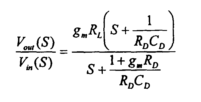
The transfer function of the
equalizer 20 in the S domain is illustrated in
equation 1 below:
The transfer function has a zero at 1/2 π RD CD. For a fixed value of the
emitter degeneration resistor RD, varying the shunt capacitance CD results in an
increase in a high frequency boost. Parasitic capacitance on the output node creates a
second high frequency pole with the load resistor RL which rolls off the high
frequency response. Due to the simplicity of the equalizer design and its
accompanying transfer function, the equalizer 20 can be designed to operate at
relatively high frequencies while consuming only nominal amounts of power and chip
area.
As will be discussed in more detail below, the equalizer 20 is adapted to
compensate for electrical cable attenuation. More particularly, as is generally known
in the art, all electrical cable is known to attenuate signals, for example, as shown in
FIG. 5. The amount of attenuation is a function of the signal frequency and the length
of the cable. The relationship to length is known to be linear while the relationship to
frequency is known to be inversely proportional to the frequency of the signal. FIGS.
4A and 4B illustrate the frequency response of both the attenuation as well as the
group delay of 30 foot of type RG-316 coaxial cable. Both the measured and model
characteristics are illustrated. FIG. 4A illustrates the signal attenuation as a function
of frequency (i.e. the S21 parameter) while FIG. 4B illustrates the group delay as a
function of frequency. As shown in FIG. 4A, the cable has somewhat of a low pass
filter characteristic. The group delay plot illustrated in FIG. 4B indicates that the
phase response is relatively linear. As will be discussed in more detail below, these
exemplary cable characteristics are amenable to being compensated by the equalizer
20 for a variety of cable lengths and data rates.
An exemplary receiver 40 incorporating the equalizer 20 in accordance
with the present invention is illustrated in FIG. 2. A corresponding schematic
diagram of the receiver 40 is illustrated in FIG. 3 with the exception that FIG. 3
illustrates a two stage equalizer. As discussed above, the receiver 40 including the
equalizer 20 in accordance with the present invention is amenable to being fabricated
monolithically using various technologies including HBT technology.
The receiver 40 includes an input impedance matching network 42. The
input matching network 42 is illustrated in FIG. 3 to provide 50Ω input impedance
matching to match the characteristic impedance of a typical coaxial cable. In the case
of single-ended connections, the receiver 40 also includes a single to differential
converter 43 since all signal processing in the equalizer 20 is done on a differential
basis. Interstage buffer amplifiers 45 and 47 are disposed on the input and output of
the equalizer 20. A slicer 49 is provided to decode whether the received signal is a
logical 1 or 0. In accordance with an important aspect of the invention, the equalizer
20 is disposed upstream of the slicer 49. By disposing the equalizer 20 upstream of
the slicer 49, the low pass attenuation affects of the cable are compensated prior to the
decoding of the received signal.
A schematic diagram of the receiver is illustrated in FIG. 3. FIG. 3
corresponds to the block diagram illustrated in FIG. 2 with the exception that two
equalizer stages 20 and 22 are provided. As shown in FIG. 4A, the signal attenuation
at 5GHz is about 24dB for 10 Gbps operation. The equalizer 20 must be able to
provide roughly this amount of boost at this frequency. In order to receive that much
frequency boost at 5GHz, two equalizer stages are required. It should be understood
by those of ordinary skill in the art that the receivers 20 and 41 illustrated in FIGS. 2
and 3 are merely exemplary and that the number of equalizers will be dependent on
the particular type of cable, the length of cable as well as the data transfer rate.
Turning to FIG. 3, the input impedance matching circuit 42 includes a
pair of differentially connected transistors 44 and 46 connected in a common emitter
configuration. A pair of resistors 48 and 50 are connected between the base and
collector terminals of the differentially connected transistors 44 and 46. The collector
terminals of the differential transistor pair 44, 46 are connected to a supply voltage
VCC. The emitter terminals are connected to a pair of common emitter configured
transistors 52, 54, whose emitters are connected to the common voltage source VEE
by way of a pair of emitter degeneration resistors 56 and 58. A constant voltage
source Vbias is applied to the base terminals of the common emitter configured
transistors 52 and 54 to provide a constant current source for each of the differentially
connected transistors 44 and 46. The input to the impedance matching network 42 is
applied to the base of the transistor 44 as indicated by Vin.
While the input to the receiver 20, 41 is single ended, all internal signal
processing is differential as discussed above. Thus, the single to differential converter
43 converts the single-ended input to a pair of differential outputs. The single to
differential converter 43 includes a pair of differentially connected transistors 60 and
62. The collectors of the differentially connected transistors 60 and 62 are connected
to the supply voltage VCC by way of a pair of resistors 64 and 66. The inputs for the
differentially connected transistor 60 and 62 are from the emitter terminals of the
transistors 44, 46 in the input impedance matching circuit 42. The differentially
connected transistors 66 and 62 are connected in a common emitter configuration and
connected to a common current source which includes a transistor 68 and a resistor
70. The collector terminals of each of the transistors 66 and 62 form the differential
inputs for the balance of the circuit.
In accordance with an important aspect of the invention, the receiver 20,
41 may include one or more equalizer stages, such as the equalizer stages 20 and 22
and interstage buffering. Interstage buffering is provided by a buffer 47 between the
equalizer stages 20 and 22. Interstage buffering is also provided by a pair of buffers
45 and 51 relative to the input and output of the equalizer stages 20 and 22. As
discussed above, the equalizers 20, 22 compensate for the low pass attenuation
characteristics of the cable.
Each of the buffers 45, 47 and 51 are configured as simple emitter
followers and perform level shifting and interstage buffering of the equalizer stages 20
and 22 to maintain high bandwidth. The buffer 45 includes a pair of transistors 72
and 74 connected to a pair of constant current sources formed from a pair of
transistors 76 and 78 and a pair of resistors 80 and 82. Similarly, the buffer 47
includes a pair of emitter follower transistors 84 and 86 connected to a pair of
constant current sources which include the transistors 88 and 90 coupled to the
common voltage source VEE by way of a pair of resistors 92 and 94. The buffer 51
is also similar and includes a pair of transistors 96 and 98 configured as emitter
followers connected to a pair of constant current sources. The constant current
sources for the buffer 51 are formed from a pair of transistors 100, 102 connected to
the common voltage source VEE by way of a pair of resistors 104 and 106.
Each equalizer stage 20, 22 includes a pair of differentially connected
transistor Q1A, Q1B and Q2A, Q2B as well as a pair of load resistors RL1, RL2.
Emitter degeneration resistors 2RD1, 2RD2 are connected between the emitter
terminals of each of the differential transistor pairs Q1A, Q1B and Q2A, Q2B. Shunt
capacitors CD 1/2 and CD2/2 are connected in parallel with the emitter degeneration
resistors 2RD1, 2RD2. Each transistor in the transistor pairs Q1A, Q1B and Q2A,
Q2B are connected to constant current sources formed from a plurality of transistors
108, 110, 112 and 114 and a plurality of resistors 116, 118, 120 and 122.
As discussed above, a slicer 49 decodes the input signal and outputs
either a logical 1 or a logical 0 voltage at its output Vout. The slicer 49 is a relatively
high gain stage with well-defined full scale output levels. The slicer 49 includes a
pair of differentially connected transistors 124, 126 connected in a common emitter
configuration. The base inputs to the differentially connected transistor pair 124 and
126 are connected to the emitter terminals of the transistors 96 and 98 forming the
interstage buffer 51. A pair of load resistors 128 and 130 are connected between the
collector terminals and the supply voltage source VCC. The common emitter terminal
of the transistor pair 124 and 126 is connected to a constant current source formed
from a transistor 132 and a resistor 134. The receiver 20, 41 may also include output
buffers (not shown), for example, to drive external electrical devices.
As discussed above, the
equalizer 20 as well as the
receivers 40 and 41
are amenable to being fabricated monolithically, for example using HBT technology.
Alternatively, the
equalizer 20 as well as the
receivers 40 and 41 may also be
fabricated using bipolar technology, for example, from bipolar junction transistors.
The exemplary receiver illustrated in FIG. 3 is adapted to be fabricated on a die
having dimensions 600 µm x 1250 µm as illustrated in FIG. 6. For the exemplary
equalizer illustrated in FIG. 3 formed from 1µm GaAs HBT technology, the
approximate active areas and power consumption of the various receiver blocks is
illustrated in the table below.
| BLOCK | AREA | POWER |
| Input match/single to differential converter | 200µm x 200µm | 42mW |
| Two stage EQ/interstage buffer | 300µm x 200µm | 52mW |
| Slicer | 100µm x 200µm | 21mW |
| Total active area Excluding output drivers | 600µm x 200µm | 116mW |
FIGS. 7A-7D are measured eye diagrams from a 250mV peak to peak
single-ended input over 30 feet of RG-316 coaxial cable. In particular, FIGS. 7A and
7C illustrate the input signal at 5 and 10 Gbps, respectively, while FIGS. 7B and 7D
illustrate the output of the equalizer. The test setup consisted of a random bit
generator connected to the exemplary receiver 40, 41 by way of a length of 30 feet of
RG-316 coaxial cable and a sampling scope to monitor the signal at the input to the
receiver 40/41 as well as at the output of the equalizer 20. An Anritsu MP1755A type
random bit generator was used to provide single-ended binary outputs with a 250 mV
peak to peak voltage swing into the coaxial cable. A Tektronix type 11801B
oscilloscope was used to measure and plot the eye diagrams at the receiver input as
well as the equalizer output. As shown from the FIGS. 7A-7D there is an increase in
jitter at 10Gbps which may be attributed to the non-ideal phase equalization in the
cable/equalizer combination. However, despite the increase in jitter, FIGS. 7B and
7D clearly indicate that the equalizer 20, in accordance with the present invention, is
effective in opening the data eye at the various data rates. At lower data rates and
shorter cable lengths, the performance is even better.
As mentioned above, the cable equalizer, in accordance with one
embodiment of the present invention, is adapted to be fabricated from heterojunction
bipolar transistor (HBT) technology which enables the equalizer to be fabricated
monolithically as well as integrated with other components to form a monolithic
receiver. The process steps for forming an equalizer in accordance with the present
invention, for example from GaAs technology, are illustrated in FIGS. 8a-8h, 9a-9f
and 10a-10c and described below. Initially, a GaAs wafer (not shown) is obtained for
use as a substrate. An alignment key structure is placed on the wafer in a well-known
fashion prior to processing. Referring to FIG. 8a, a vertical stack of semiconductor
layers for example, a sub-collector layer 142, a collector layer 144, a collector layer
144, a base layer 146 and an emitter layer 148 are grown on top of substrate layer 150
(FIG. 9a), for example, by molecular beam epitaxy (MBE). Subsequently, as
illustrated in FIG. 8b, an emitter mesa 152 with a nitride layer 154 is formed by
conventional photolithography techniques and etched. In particular, the emitter mesa
152 may be formed by wet chemical etching techniques to form the undercuts as
shown relative to the nitride layer 154. The nitride is etched by dry etching
techniques. An emitter photoresist 156 is spun on top of the structure and developed
with a slight overhang as shown in FIG. 8b. As discussed in more detail below, the
emitter photoresist layer 156 is used in part to provide automatic spacing of the base
ohmic contacts 158 and 160 as shown in FIG. 8c. An additional layer of photoresist
164 is spun off the device as shown in FIG. 8c. The photoresist, for example, self-aligned
base metal (SABM), is developed by conventional techniques and in
cooperation with the emitter photoresist layer 156 determines the location of the base
ohmic metal contacts 158 and 160. After the SABM photoresist layer 164 is
developed and exposed, the base metal ohmic contacts is deposited on the structure.
The excess metal layer 166 and photoresist 164 are lifted off by conventional
techniques as illustrated in FIG. 8d, leaving the base ohmic metal contacts 158 and
160.
Subsequently, as shown in FIG. 8e, the nitride layer 154 is etched
completely off the emitter mesa 152. Subsequently, a second nitride layer 162 is
deposited on the device. In preparation of the formation of non-ohmic contacts as
discussed below, a photoresist 165 is spun onto the device in preparation for
formation of the collector ohmic metal contacts, as generally shown in FIG. 8e. As
shown, FIG. 8f, the photoresist layer 165 is exposed and developed in a conventional
manner in preparation of a base mesa etch. In particular, as shown in FIG. 8f, the
second nitride layer 162 is etched followed by etching of the base layer 146 and
collector layer 144 to form a base mesa 167. The photoresist 165 is then stripped by
conventional techniques resulting in the structure illustrated in FIG. 8f.
Another photoresist layer 168 is spun onto the device as shown in FIG.
8g. The photoresist layer 168 is patterned and developed to locate the collector ohmic
contact 170. A collector ohmic metal layer 172 is deposited on the device and lifted
off by conventional techniques as shown in FIG. 8h to form the collector ohmic metal
contact 170.
Next, isolation regions are formed in the device. These isolation regions
formed by way of a photoresist layer 174 which is spun onto the device. The
photoresist 174 is patterned and exposed as shown in FIG. 9a. Boron ions, for
example, are implanted into the device to form the isolation regions. A thin film
resistor may optionally be formed on the device. The thin film resistor may be
formed by stripping the photoresist layer 174 applied in FIG. 9a and depositing
another silicon nitride layer 180. After the silicon nitride layer 180 is deposited on
the device, another photoresist layer 182 is spun on the device as illustrated in FIG.
9b. The photoresist layer 182 may be used to define the location of the thin film
resistor 194. The thin film resistor may be formed by depositing a CERMET film
194, for example (CrSIO), on top of the device is generally shown in FIG. 9b. The
excess metal and photoresist are removed by conventional techniques as shown in
FIG. 9c, leaving the thin film resistor and the structure as basically shown in FIG. 9c.
Another photoresist (not shown) is spun on top of the device to define
the locations of the interconnect metal. The nitride layer 180 is etched as shown in
FIG. 9d. A photoresist 188 is applied to the device as shown in FIG. 9e and
patterned to define the interconnect metals. The photoresist 188 is developed in a
conventional matter in a layer of interconnect metal 190, for example Ti/Pt/Au/Ti, is
deposited on the device as generally shown in FIG. 9e. The excess metal and
photoresist layer 188 are lifted off by conventional techniques. Subsequently, a fourth
nitride layer 192 is deposited as shown in FIG. 9f. As shown in FIG. 10a, vias 196
and 198 are formed in the interconnect metal layer. These vias 196 and 198 are
formed by spinning a photoresist on top of the device; patterning the photoresist with
conventional techniques to define the vias 196 and 198; developing the photoresist and
subsequently etching the nitride layer 150 to form the vias 196 and 198, as generally
shown in FIG. 10a. Next, as shown in FIG. 10b, an air bridge is formed. The air
bridge is formed by spinning a photoresist 200 on top of the device and patterning the
photoresist to form an air bridge. A metal layer 202 is then deposited on top of the
photoresist 200 to form the air bridge. The photoresist is then removed by
conventional techniques. A passivation pattern nitride layer may be deposited on the
device. A photoresist may be used to form the dice streets to enable the chips to be
diced.
Obviously, many modifications and variations of the present invention
are possible in light of the above teachings. Thus, it is to be understood that, within
the scope of the appended claims, the invention may be practiced otherwise than as
specifically described above.
What is claimed and desired to be covered by a Letters Patent is as
follows: