EP1030458A2 - Wideband parallel processing digital tuner - Google Patents
Wideband parallel processing digital tuner Download PDFInfo
- Publication number
- EP1030458A2 EP1030458A2 EP00102866A EP00102866A EP1030458A2 EP 1030458 A2 EP1030458 A2 EP 1030458A2 EP 00102866 A EP00102866 A EP 00102866A EP 00102866 A EP00102866 A EP 00102866A EP 1030458 A2 EP1030458 A2 EP 1030458A2
- Authority
- EP
- European Patent Office
- Prior art keywords
- filters
- wideband
- digital
- recited
- tuner
- Prior art date
- Legal status (The legal status is an assumption and is not a legal conclusion. Google has not performed a legal analysis and makes no representation as to the accuracy of the status listed.)
- Withdrawn
Links
Images






Classifications
-
- H—ELECTRICITY
- H04—ELECTRIC COMMUNICATION TECHNIQUE
- H04B—TRANSMISSION
- H04B1/00—Details of transmission systems, not covered by a single one of groups H04B3/00 - H04B13/00; Details of transmission systems not characterised by the medium used for transmission
- H04B1/06—Receivers
- H04B1/16—Circuits
- H04B1/26—Circuits for superheterodyne receivers
- H04B1/28—Circuits for superheterodyne receivers the receiver comprising at least one semiconductor device having three or more electrodes
-
- H—ELECTRICITY
- H04—ELECTRIC COMMUNICATION TECHNIQUE
- H04B—TRANSMISSION
- H04B1/00—Details of transmission systems, not covered by a single one of groups H04B3/00 - H04B13/00; Details of transmission systems not characterised by the medium used for transmission
Definitions
- This invention relates generally to tuner circuits in data communications systems.
- the present invention relates to a wide-band digital tuner in a communications satellite.
- a tuner in general, is capable of down converting from any frequency within a specified frequency range.
- the tuners in satellite data transmission systems are usually analog or digital with a single serial input received from the output of an analog-to-digital converter (ADC).
- ADC analog-to-digital converter
- ADC analog to digital converter
- the tuner 14 receives the digitized signal IF in outputted by the analog to digital converter 12 and processes it into quadrature signal processing paths 16 and 18 which each contain a frequency converter 20 which downwardly shifts the input signal IF in to a lower frequency.
- the frequency converters 20 of the I signal processing path 16 and the Q signal processing path 18 respectively receive input carriers COS( ⁇ T) and SIN( ⁇ T) from the quadrature digital sinewave generator which cause the frequency converters to produce the quadrature I and Q signals which are downshifted in frequency to a lower carrier frequency.
- the input to the quadrature digital sinewave generator 22 is a frequency command F in which commands the quadrature digital sinewave generator 22 to output the quadrature carriers COS( ⁇ T) and SIN( ⁇ T) of the appropriate frequency to cause the frequency converters to shift the input signal IF in to the lower carrier frequency for further signal processing.
- the envelopes of the lower frequency quadrature carriers produced by connection of COS( ⁇ T) and SIN( ⁇ T) to the frequency converters 20 are modulated with the quadrature components of data present in the intermediate frequency input signal IF in .
- the outputs from the frequency converters 20 are applied to suitable low pass filters 24 which attenuate frequency components outside the desired lower carrier frequency band to which the I and Q data components are shifted. (Alternatively, tuner 14 could utilize bandpass filters instead of lowpass filters 24.)
- the output I and Q signals are applied to downstream demodulator processing 26 of a conventional nature including channelization, discrete Fourier transformation (DFT) and other known signal processing techniques.
- DFT discrete Fourier transformation
- the bandwidth of tuner 14 is limited and switching between multiple IF frequencies is typically accomplished before the payload is converted in ADC 12 to the single serial digital signal provided to tuner 14.
- These multiple IF frequencies may, but need not, be located at uniformly-spaced positions in frequency.
- the process of switching between different IF frequencies is sometimes referred to as "hopping".
- hopping is often performed in a quick random pattern known only to the transmitting and receiving stations.
- Analog components impart the disadvantages of signal attenuation, heightened noise and lower reliability. These problems are exacerbated when the data transmission system utilizes frequency hopping among different channels.
- Channelizers are commonly used to separate an input wideband signal of a specific spectrum received from an antennae into a plurality of narrowband channels.
- the wideband signal may carry different channels using different frequency bands, different time slots, different spread spectrum coding, or a combination of any two or more of these techniques.
- the channelizers may be wideband channelizers and/or narrowband channelizers used to separate a wideband signal into smaller sections of constituent channels.
- the channel distribution in a wideband satellite communications application may be a plurality of 2 GHz channel groups, each comprised of twenty (20) 100 MHz sub-band channels, or 320 MHz channel groups, each comprised of four (4) 80 MHz sub-band channels.
- Each sub-band channel in these implementations may be channelized into smaller sections of narrower band channels, such as, for example, four (4) narrowband channels of 20 MHz each.
- narrowband signals are limited to any particular spectral range and may separately determined for different applications.
- a preferred application of the present invention is in a wideband satellite communications system transmitting payload data over a number of different frequency channels at extremely high data rates.
- it also has application to any frequency-hopped communications system in which the transmitted waveform requires dehopping.
- it may be used to prepare channel information from a waveform containing channels at non-uniformly spaced frequencies.
- a communications satellite has an analog front-end, an ADC located functionally "closer” to the antennae, and a serial-to-parallel converter, also known as a demultiplexer or demux, providing several digital output signals in parallel.
- the analog front-end is simplified to perform a coarse tuning or "de-hop", thus avoiding many of the disadvantages associated with the conventional analog front-end.
- the ADC is a modern commercially available unit or a specially designed unit able to sample at extremely high speed data rates.
- the single input from the ADC is quickly switched by the demux to a number of output branches. Each output switch outputs at a slower rate than the ADC even though the aggregate rate remains the same. This reduction in data sampling rate permits the processing of wide bandwidth signals resulting from coarse tuning.
- the fine tuning is performed in an advanced digital tuner receiving the plurality of parallel digital signals inputs from the demultiplexer.
- Parallel architecture and processing in the advanced digital tuner allows the high sample rate data to be processed at a much slower clock rate.
- the digital tuner filters out half of the spectrum with a complex band-pass filter, such as a Hilbert Transform filter, and down converts the other half to complex baseband.
- An alternative architecture would allow downconversion first and then filtering out half of the spectrum with a half-band filter. Because the "half-spectrum" is less than one-half of the Nyquist rate, the tuner can down sample by 2 and no aliasing occurs. This prepares the output signal from the tuner for downstream demodulator processing such as channelization and data detection
- Fig. 2 is a block diagram of the major components of the receiving circuitry in a wideband communications device such as, but not limited to, a satellite.
- a wideband communications device such as, but not limited to, a satellite.
- input devices may be used for intercepting or capturing electromagnetic radiation for subsequent input and down conversion in the exemplary receiver. Examples of such input devices may include antennas, waveguides, coaxial cables, optical fibers, or infrared frequency transducers.
- an exemplary wideband, high data rate, communications satellite receiver may comprise an analog front end section 10 which downconverts the received frequencies and extracts a selected frequency spectrum.
- the passed wideband signal may inherently contain a plurality of narrowband channels.
- the analog front end section 10 may be controlled in such a manner that it sequentially selects frequency spectrums of interest to carry out a hopping procedure. It also performs a coarse tuning of the received frequencies.
- a high-speed ADC converter 12 samples the wideband signal at a sampling rate set within the Nyquist criterion of at least twice the highest desired frequency to produce a digitized signal.
- the digitized signal may be represented by a sequence of n-bit data samples, where n>0.
- the sequence of n-bit data samples produced by ADC 12 is input to demultiplexer 13, which may produce a plurality of parallel data outputs 13 1 -13 n .
- the demultiplexer may be implemented as a multiple tapped delay line with each parallel output being outputted from a different tap of the delay line.
- the input samples of the demultiplexer are inputted serially at the ADC sampling rate and outputted in parallel at a slower rate.
- the demultiplexed data outputs 13 1 -13 n of the demultiplexer 13 may be applied to an advanced digital tuner 14' constructed according to the principles of the present invention.
- the advanced digital tuner 14' converts the demultiplexed data outputs 13 1 -13 n of the demultiplexer 13 from real data to complex (real and imaginary) data representations.
- the output of advanced digital tuner 14' can be forwarded, for example, to a channelizer for separation into a plurality of narrowband channels, where each narrowband channel may convey one of the channels conveyed by the wideband signal, and/or to other types of signal processing circuits (not shown).
- the advanced digital tuner 14' uses a parallel architecture of filter blocks to process digital data from ADC 12 at sample rates which are, for example, in the gigabit per second range.
- the sample rates may be higher or lower, of course, depending on the speed of the implementing technology.
- a filter block encompasses a filter which greatly attenuates nearly one half of the wide bandwidth digital spectrum of the incoming digital signal, places the remaining half at complex baseband and down samples by 2. There is no aliasing since the complex baseband signal is less than one-half the Nyquist rate and since the filter greatly attenuates the spectrum where aliasing would have occurred.
- a detailed description of the parallel architecture of tuner 14' is provided later in this description. But first, two separate embodiments of the filter blocks utilized in the parallel architecture are now described.
- FIG. 3 A first exemplary embodiment of a filter block in advanced digital tuner 14' according to the present invention is illustrated in a simplified form in Fig. 3. It should be understood that separate I and Q channels are present in Fig. 3 but have been omitted to simplify the illustration.
- the filter block in Fig. 3 receives only one stream of samples from the output signals 13 1 -13 n of demultiplexer 13 as an input data signal.
- the branches of demultiplexer 13 provide an interleaved stream of samples, e.g., x0, x4, x8, x12, etc. for a 1-to-4 DEMUX.
- the input data signal is applied to a frequency converter 36 where it is multiplied by a complex sinusoidal waveform to shift it to a lower carrier frequency.
- the signal is then filtered by a halfband filter (HBF) 37, a special lowpass filter as exemplified in Fig. 5.
- the output of halfband filter 37 is then down sampled by 2 in down sampler 42. Finally, the signal undergoes a selected frequency shift in F s /4 shift circuit 44.
- Figs. 4a - 4d The frequency band operation of the first embodiment is illustrated in Figs. 4a - 4d.
- Fig. 4a shows the frequency band content of the input signal to the filter block after the ADC and demuxing operations.
- Fig. 4b shows the band content after the frequency shift (multiplying by sinusoid) and applying of the HBF 37.
- Figs. 4c and 4d then show the bands after down sampling and F s /4 shift.
- Fig. 5 shows the transcripts of two runs of a computer program used to design and create the half-band filter 37 using the Chebyshev (equi-ripple) error criterion and the Parks-McClellan algorithm.
- the runs show the respective characteristics of 15-tap and 19-tap half-band filters with equal single-sided 160 MHz pass band, transition band, and stop band.
- the 15-tap filter has a 0.03 dB pass band ripple and -49.1 dB stop band rejection, while the 19-tap filter has a 0.01 dB pass band ripple and a -59.5 dB stop band rejection.
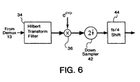
- FIG. 6 A second preferred embodiment of the filter block of an advanced digital tuner according to the present invention is illustrated in simplified form in Fig. 6. It is similar to the first embodiment except that it uses a Hilbert Transform Filter (HTF) 34 before the frequency converter 36, instead of a half-band filter 37 after the frequency converter 36.
- HTF Hilbert Transform Filter
- Hilbert Transform Filters are known to those in the art.
- the Hilbert Transform Filter (HTF) 34 converts real data input signals 13 1 -13 n into complex data signals with real and imaginary components, and greatly attenuates nearly one half of the wideband digital spectrum of the signal.
- the imaginary part of the Fourier Transform of a complex signal is the real part phase-shifted by -90 degrees. Therefore, to create a complex signal from a real signal, the real signal is simply passed through an HTF with the above response. The output represents the imaginary part of the newly created complex signal. The original signal is delayed by the group delay of the HTF and is used as the real part of the final output. In the frequency domain, the created signal has a one-sided spectrum, equivalent to one side of the original signal's spectrum.
- At least one digital frequency synthesizer 38 in the filter block supplies digitally synthesized quadrature sinusoidal waveforms, representing a complex exponential, to the frequency converter 36.
- the sinusoids are then multiplied with the data output from HTF 34 to modulate them downwardly to complex baseband.
- the particular specified frequency to which the data outputted from HTF 34 is shifted down is specified by the input FREQUENCY CONTROL WORD 40.
- the output from the frequency converter is down sampled by a factor of 2 by down sampler 42 which eliminates the excess half of the data samples.
- the circuit thus operates as a decimation as well as a tuner.
- the output of down sampler 42 is applied to a frequency shift 44 which shifts up the frequency of the output from the down sampler 42 by a frequency shift equal to one quarter of data sampling rate F s .
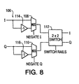
- a frequency shift controller 45 produces control signals SWITCH RAILS, NEGATE Q and NEGATE I which operate in accordance with the relationship set forth in the table below to produce a cyclical output of +1, +j, -1 and -j which is clocked at the data sampling rate F s .
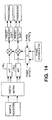
- the circuitry for generating the control signals is discussed below in conjunction with Fig. 8. Multiplier Control Signals +1 do not negate, nor swap rails +j negate Q-rail, swap rails (i.e. I and Q are switched) -1 negate both rails, do not swap rails -j negate I-rail, swap rails
- the frequency shift 44 outputs I and Q data signals which are shifted to a correct frequency position to align the I and Q data in frequency with channels to be produced by a channelizer (not shown).
- the digital spectrum produced by the frequency conversion 36 has channels positively and negatively spaced about baseband but does not have a channel at baseband.
- a channelizer requires alignment of the input data with a channel centered at baseband in order to function properly.
- the frequency shift 44 is further capable of performing a frequency shift equal to one quarter, one half, or zero, of the data sampling rate F s , where F s is the data sample rate of data outputted from the down sampler 42.
- the frequency shift is flexible in terms of which frequencies it can shift to and from. It positions the waveform for the next stage, such as channelization.
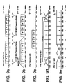
- Figs. 9a - 9e The frequency band operation of the second embodiment is illustrated in Figs. 9a - 9e.
- Fig. 9a shows the frequency band content of the input signal to the filter block after the ADC and demuxing operations.
- Fig. 9b shows the band content after applying HTF 34.
- Fig. 9c shows the band content after frequency shift (multiplying by sinusoid).
- Figs. 9d and 9e then show the bands after down sampling and F s /4 shift, respectively.
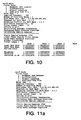
- Fig. 10 is a transcript of a run of the same computer program utilized in Fig. 5, and shows a Hilbert Transform Filter with the same two-sided pass band bandwidth and 19 taps as the half-band filter in the first embodiment of the filter block.
- the pass band ripple and stop band rejection are slightly worse than those of the first embodiment.
- Figs. 11A-11C are run transcripts which show how many taps are required to achieve the filter characteristics of the 19-tap half-band filter of the first embodiment. It can be seen that the run extends from 19 taps to 35 taps in order to achieve nearly identical filter characteristics.
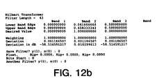
- Figs. 12A and 12B take into consideration a 10 MHz offset and widens the pass band. Although HTF 34 can be made into a general, non-symmetric, complex band-pass filter, then every tap value will become non-zero, implying a large increase in hardware for implementation.
- the second embodiment of the filter block exploits the symmetry and zero-valued-taps of the Hilbert Transform Filter as well as the down sampling by 2 to achieve an efficient implementation, provide a more compact filter design (lower gate count) and more efficient power usage.
- the down sampling and filter characteristics also provide a method of efficient input ordering and data storage.
- the tuner can be partitioned such that only half of the implementation requires a unique design. The other half is a hardware copy of the first, thereby shortening design and test time.
- tuner 14' an important feature of the preferred embodiments of tuner 14' is the parallel architecture in which the filter blocks are implemented.
- a respective filter block could be provided for an equal number of the output signals 13 1 -13 n of the demultiplexer 13 input to the tuner 14'.
- the number of filter blocks and hence filters, frequency synthesizers, multipliers, etc.
- the number of filter blocks is either greater than, equal to, or less than the number of output signals of the demultiplexer.
- the tuner 14' in accordance with the preferred embodiments of the invention utilizes a strategic combination of elements rather than the mere repetition of a filter block for each signal input into the tuner. Furthermore, the tuner operates in a pipeline fashion. As one sample enters a filter as input, one output sample must be generated. The filter blocks in tuner 14' span multiple input samples in each clock cycle to generate that single output sample. The invention parallelizes the processing by having many filters operating on data simultaneously. The tuner store those samples it needs to determine the outputs of the parallel processed filters in a collection of sample registers and each filter spans a multiple number of input samples from different output branches of demultiplexer 13.
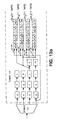
- tuner 14' Exemplary embodiments of tuner 14' are shown in Figs. 13a and 13b.
- demultiplexer 13 is a 1-to-4 demultiplexer having only four (4) output signals and that HTF filters 34 have only 11 taps.
- the tuner includes a number of sample registers, each sample register connected to a respective output signal of demultiplexer 13 or in series to a sample register connected to a respective output signal of demultiplexer 13. As a group of four samples are read into the first sample register in a series of sample registers, the samples are read out of the last sample register in a series of sample registers. If one output sample is processed for every input sample, a succession of filtering operations can be obtained which are shifted by one input sample.
- a group of four successive outputs can be obtained all at the same time as long as there are sufficient and the input samples can feed those filtering operations. (It is impossible to filter individual branches of the DEMUX, since the DEMUX branches would provide interleaved samples, e.g., x0, x4, x8, x12, etc. for a 1-to-4 DEMUX.)
- demultiplexer 13 simply provides a series of sequential samples (a-m) in time multiplexed fashion
- the sample registers store the samples respectively as shown in Figs. 13a and 13b. This process of storing the samples creates a bank of samples so that they can be provided at the appropriate time to the appropriate filter.
- a connection matrix is formed so that the sample stored in each sample register can be selectively provided to any one of the Hilbert Transform Filters. The samples are then provided to the Hilbert Transform filters at the proper timing and input position.
- the sequence of connections can be determined and the connection matrix controlled so that the proper order and sequence of connections is carried out.
- Fig. 13a Without down sampling, four filters are utilized as shown in Fig. 13a. If four input samples came into the filters from the DEMUX, implying that the filter rate is 4 times slower than the ADC sampling rate, then 4 output samples need to be determined during that same time to prevent data overflow or underflow. Not all 10 samples are used in every filter, and potentially need to be stored for the next cycle of filter operations. This is implemented in the switch fabric for linking the correct input samples to the appropriate filters.
- Both Hilbert Transform Filters and Half-Band Filters are symmetric finite-impulse response filters; one half is the mirror image of the other half. Hence, by "pre-folding" the inputs, i.e. adding them appropriately prior to the filtering operation, the number of taps can be reduced by 2. Secondly, if they have an odd number of taps, every other tap has a value of zero. This reduces the number of unique tap values to process by another factor of 2.
- DA distributed arithmetic
- All process bits can be processed in one clock cycle.
- frequency shift control can negate filter outputs as necessary when configuring the Hilbert Transform Filter to choose which side-band, positive or negative, is passed and which side-band is rejected.
- the complex exponential that multiplies the signal to down convert it in frequency is preferably implemented with a digital direct frequency synthesizer (DDFS).
- DDFS maps a phase index (integers representing phase increments) to the amplitude of a sinusoidal signal having that particular phase.
- phase index increments in constant intervals
- a frequency is represented, and the output of the DDFS forms a sinusoidal signal.
- the DDFS produces both sine and cosine outputs to duplicate the complex exponential.
- a common phase accumulator holds the respective phase index for each DDFS.
- the input samples are multiplied individually by samples of a sinusoid that represent different phases. In this way, the frequency does not change. Just as the phase interval between any two consecutive samples is identical, the phase interval between samples separated by N samples is identical. Hence, only constant offsets are required for each individual DDFS.
- Each complex multiplier also has a unique architecture. It does not perform the conventional (ad-bc) + j(ac+bd) computation where 4 multiplies and two adds are necessary.
- the F s /4 frequency shift circuitry does not have to be redundantly provided for each branch. Since the down sampling may be accommodated in the filtering operations, it is not necessary to provide the entire selectable frequency shift circuit and controller shown in Fig. 8 for each filter output. Instead, it is possible to a priori set the appropriate shift (either 1, -1, j or -j) for each filter branch.
Landscapes
- Engineering & Computer Science (AREA)
- Computer Networks & Wireless Communication (AREA)
- Signal Processing (AREA)
- Circuits Of Receivers In General (AREA)
- Digital Transmission Methods That Use Modulated Carrier Waves (AREA)
Abstract
Description

| Multiplier | Control Signals |
| +1 | do not negate, nor swap rails |
| +j | negate Q-rail, swap rails (i.e. I and Q are switched) |
| -1 | negate both rails, do not swap rails |
| -j | negate I-rail, swap rails |
Claims (16)
- A wideband digital tuner comprising:a demultiplexer circuit receiving a high rate wideband digital signal and outputting a plurality (n) of parallel digital signals, each of the parallel digital signals having a rate which is 1/n the rate of the high rate wideband digital signal;a bank of sample registers, each sample register storing one sample of the high rate wideband digital signal;a plurality of filters, said plurality of filters attenuating one half of the wideband digital signal spectrum;a connection matrix connecting the bank of sample registers and said plurality of filters, the connection matrix simultaneously providing each of said plurality of filters with a respective one of the samples stored in said bank of sample registers; andat least two frequency shift circuits, each for shifting the output of one of said plurality of filters.
- The wideband digital tuner recited in claim 1, wherein said plurality of filters comprise Hilbert Transform filters.
- The wideband digital tuner recited in claim 1, wherein said plurality of filters comprise complex bandpass filters.
- The wideband digital tuner recited in claim 1, wherein the number of filters is less than the number of parallel data signals output by the demultiplexer.
- The wideband digital tuner recited in claim 4, wherein the samples are decimated by down sampling performed by said plurality of filters.
- The wideband digital tuner recited in claim 1, wherein the frequency shift circuit is configurable to perform a selectable frequency shift.
- A wideband communications receiver comprising:an antenna;an analog bandpass filter filtering the analog signal received by the antenna;a high speed analog-to-digital converter converting the filtered analog signal to a digital signal;a demultiplexer converting the digital signal to a plurality (n) of parallel digital signals, the data rate of the parallel digital signals being 1/n of the rate of the digital signal;at least two filters connected to the parallel digital signals, the filters attenuating one half of the wideband digital signal spectrum; andat least one processing circuit processing the outputs of said at least two filters.
- A wideband communications receiver as recited in claim 7, further comprising a connection matrix connecting the bank of sample registers and said at least two filters, the connection matrix simultaneously providing each of said at least two filters with a respective one of the samples stored in said bank of sample registers; andat least two frequency shift circuits, each for shifting the output of one of said at least two filters.
- The wideband communications receiver recited in claim 7, wherein the number of filters is less than the number of parallel data signals output by the demultiplexer.
- The wideband communications receiver recited in claim 9, wherein the samples are decimated by down sampling performed by said at least two filters.
- The wideband communications receiver recited in claim 8, wherein the frequency shift circuit is configurable to perform a selectable frequency shift.
- The wideband communications receiver recited in claim 7, wherein the processing circuit comprises a channelizer.
- The wideband communications receiver recited in claim 7, wherein the receiver sequentially switches between a number of different frequencies.
- The wideband communications receiver recited in claim 13, wherein the analog bandpass filter performs a coarse tuning and said at least two filters perform a fine tuning of the signal passed by the analog bandpass filter.
- The wideband communications receiver recited in claim 7, further comprising a plurality of complex multiplexers respectively corresponding to the plurality of filters and placing the remaining half of the incoming wideband digital signal spectrums at complex baseband, at least one complex multiplexer being configured to perform only 3 multiplication operations.
- The wideband communications receiver recited in claim 15, wherein each one of the plurality of complex multiplexers comprises a digital frequency synthesizer, the digital frequency synthesizers sharing a common phase accumulator.
Applications Claiming Priority (2)
| Application Number | Priority Date | Filing Date | Title |
|---|---|---|---|
| US09/249,904 US6263195B1 (en) | 1999-02-12 | 1999-02-12 | Wideband parallel processing digital tuner |
| US249904 | 1999-02-12 |
Publications (2)
| Publication Number | Publication Date |
|---|---|
| EP1030458A2 true EP1030458A2 (en) | 2000-08-23 |
| EP1030458A3 EP1030458A3 (en) | 2003-01-29 |
Family
ID=22945509
Family Applications (1)
| Application Number | Title | Priority Date | Filing Date |
|---|---|---|---|
| EP00102866A Withdrawn EP1030458A3 (en) | 1999-02-12 | 2000-02-11 | Wideband parallel processing digital tuner |
Country Status (4)
| Country | Link |
|---|---|
| US (1) | US6263195B1 (en) |
| EP (1) | EP1030458A3 (en) |
| JP (1) | JP2000244368A (en) |
| CA (1) | CA2296968A1 (en) |
Cited By (5)
| Publication number | Priority date | Publication date | Assignee | Title |
|---|---|---|---|---|
| GB2382961A (en) * | 2001-12-05 | 2003-06-11 | Matsushita Electric Industrial Co Ltd | Multirate digital transceiver |
| WO2004082189A3 (en) * | 2003-03-10 | 2004-12-29 | Thomson Licensing Sa | Receiver and method for concurrent receiving of multiple channels |
| FR2937812A1 (en) * | 2008-10-28 | 2010-04-30 | Thales Sa | TRANSPONDER AND ASSOCIATED SIGNAL REPRODUCTION METHOD |
| CN102281096A (en) * | 2011-08-31 | 2011-12-14 | 西安空间无线电技术研究所 | Resource multiplexing digital channelized implementation system |
| EP3113371A1 (en) * | 2015-07-01 | 2017-01-04 | Televés, S.A. | System for amplifying telecommunication signals |
Families Citing this family (24)
| Publication number | Priority date | Publication date | Assignee | Title |
|---|---|---|---|---|
| AU2820701A (en) * | 2000-01-18 | 2001-07-31 | National Research Council Of Canada | Parallel correlator archtitecture |
| US6694488B1 (en) * | 2000-03-03 | 2004-02-17 | Nec Corporation | System for the design of high-performance communication architecture for system-on-chips using communication architecture tuners |
| US20020056135A1 (en) * | 2000-03-06 | 2002-05-09 | Alok Sharma | Transceiver channel bank with reduced connector density |
| US7149223B2 (en) * | 2000-03-06 | 2006-12-12 | Juniper Networks, Inc. | Enhanced fiber nodes with CMTS capability |
| US7099340B2 (en) * | 2000-03-06 | 2006-08-29 | Juniper Networks, Inc. | Enhanced CMTS for reliability, availability, and serviceability |
| US6993016B1 (en) | 2000-11-16 | 2006-01-31 | Juniper Networks, Inc. | Methods and apparatus for transmission of analog channels over digital packet networks |
| ATE341854T1 (en) | 2000-12-13 | 2006-10-15 | Juniper Networks Inc | TUNER FOR DIGITAL RECEIVER WITH MULTIPLE INPUT CHANNELS AND OUTPUT CHANNELS |
| US20020193090A1 (en) * | 2001-05-23 | 2002-12-19 | Sugar Gary L. | System and method for dynamic sampling rate adjustment to minimize power consumption in wideband radios |
| JP4682448B2 (en) * | 2001-05-25 | 2011-05-11 | 株式会社豊田中央研究所 | Receiver |
| US6704372B2 (en) * | 2001-09-18 | 2004-03-09 | Broadlogic Network Technologies Inc. | Digital implementation of multi-channel demodulators |
| US7627817B2 (en) * | 2003-02-21 | 2009-12-01 | Motionpoint Corporation | Analyzing web site for translation |
| US7425995B2 (en) * | 2003-02-28 | 2008-09-16 | Silicon Laboratories, Inc. | Tuner using a direct digital frequency synthesizer, television receiver using such a tuner, and method therefor |
| US7447493B2 (en) * | 2003-02-28 | 2008-11-04 | Silicon Laboratories, Inc. | Tuner suitable for integration and method for tuning a radio frequency signal |
| KR20050115258A (en) * | 2003-02-28 | 2005-12-07 | 실리콘 래버래토리즈 , 인코포레이티드 | Tuner for radio frequency and associated method |
| US7430254B1 (en) | 2003-08-06 | 2008-09-30 | Lockheed Martin Corporation | Matched detector/channelizer with adaptive threshold |
| EP1533916A1 (en) * | 2003-11-18 | 2005-05-25 | Mitsubishi Electric Information Technology Centre Europe B.V. | Diversity switch combiner |
| EP1533917A1 (en) * | 2003-11-18 | 2005-05-25 | Mitsubishi Electric Information Technology Centre Europe B.V. | Antenna diversity switch for a receiver system and method using this switch |
| US7903764B2 (en) * | 2004-05-10 | 2011-03-08 | Broadcom Corporation | Integrated burst FSK receiver |
| US7672268B2 (en) | 2004-06-18 | 2010-03-02 | Kenneth Stanwood | Systems and methods for implementing double wide channels in a communication system |
| US8543012B2 (en) * | 2010-05-14 | 2013-09-24 | Verizon Patent And Licensing Inc. | Compensating for end-to-end group delay ripples |
| US8792008B2 (en) * | 2011-09-08 | 2014-07-29 | Maxlinear, Inc. | Method and apparatus for spectrum monitoring |
| US8711995B2 (en) | 2011-12-22 | 2014-04-29 | Landis+ Gyr Technologies, LLC | Powerline communication receiver |
| US11290903B2 (en) * | 2019-07-17 | 2022-03-29 | SiTune Corporation | Spectrum monitoring |
| CN113472354A (en) * | 2021-07-23 | 2021-10-01 | 杭州万高科技股份有限公司 | Synchronous sampling method, device, equipment and medium for multipath signals |
Family Cites Families (11)
| Publication number | Priority date | Publication date | Assignee | Title |
|---|---|---|---|---|
| US4316282A (en) * | 1979-11-23 | 1982-02-16 | Rca Corporation | Multichannel frequency translation of sampled waveforms by decimation and interpolation |
| US4785447A (en) * | 1987-02-17 | 1988-11-15 | Nec Corporation | FDM demultiplexer using oversampled digital filters |
| US5247515A (en) * | 1991-01-28 | 1993-09-21 | Rockwell International Corporation | Apparatus for extracting one from many multiplexed signals |
| US5535240A (en) * | 1993-10-29 | 1996-07-09 | Airnet Communications Corporation | Transceiver apparatus employing wideband FFT channelizer and inverse FFT combiner for multichannel communication network |
| US5590156A (en) * | 1994-04-22 | 1996-12-31 | Carney; Ronald | Multichannel wideband digital receiver making use of multiple wideband tuners having individually selectable gains to extend overall system dynamic range |
| CA2191721C (en) * | 1994-06-01 | 2003-05-20 | Ronald R. Carney | Wideband wireless basestation making use of time division multiple-access bus to effect switchable connections to modulator/demodulator resources |
| US5592480A (en) * | 1995-03-13 | 1997-01-07 | Carney; Ronald R. | Wideband wireless basestation making use of time division multiple-access bus having selectable number of time slots and frame synchronization to support different modulation standards |
| US5577031A (en) * | 1995-03-22 | 1996-11-19 | Smith; Jeffrey W. | Wideband channelizer incorporating diversity switch |
| AU7681596A (en) * | 1995-12-11 | 1997-07-03 | Airnet Communications Corporation | Multichannel broadband transceiver system making use of a distributed control architecture for digital signal processor array |
| US6112086A (en) * | 1997-02-25 | 2000-08-29 | Adc Telecommunications, Inc. | Scanning RSSI receiver system using inverse fast fourier transforms for a cellular communications system with centralized base stations and distributed antenna units |
| US6147713A (en) * | 1998-03-09 | 2000-11-14 | General Instrument Corporation | Digital signal processor for multistandard television reception |
-
1999
- 1999-02-12 US US09/249,904 patent/US6263195B1/en not_active Expired - Lifetime
-
2000
- 2000-01-25 CA CA002296968A patent/CA2296968A1/en not_active Abandoned
- 2000-02-11 EP EP00102866A patent/EP1030458A3/en not_active Withdrawn
- 2000-02-14 JP JP2000034877A patent/JP2000244368A/en active Pending
Cited By (10)
| Publication number | Priority date | Publication date | Assignee | Title |
|---|---|---|---|---|
| GB2382961A (en) * | 2001-12-05 | 2003-06-11 | Matsushita Electric Industrial Co Ltd | Multirate digital transceiver |
| GB2382961B (en) * | 2001-12-05 | 2005-01-19 | Matsushita Electric Industrial Co Ltd | Multirate digital transceiver |
| GB2405061A (en) * | 2001-12-05 | 2005-02-16 | Matsushita Electric Industrial Co Ltd | Multirate digital transceiver |
| GB2405061B (en) * | 2001-12-05 | 2005-05-18 | Matsushita Electric Industrial Co Ltd | Multirate digital transceiver |
| US7616720B2 (en) | 2001-12-05 | 2009-11-10 | Panasonic Corporation | Multirate digital transceiver |
| WO2004082189A3 (en) * | 2003-03-10 | 2004-12-29 | Thomson Licensing Sa | Receiver and method for concurrent receiving of multiple channels |
| FR2937812A1 (en) * | 2008-10-28 | 2010-04-30 | Thales Sa | TRANSPONDER AND ASSOCIATED SIGNAL REPRODUCTION METHOD |
| CN102281096A (en) * | 2011-08-31 | 2011-12-14 | 西安空间无线电技术研究所 | Resource multiplexing digital channelized implementation system |
| CN102281096B (en) * | 2011-08-31 | 2014-01-15 | 西安空间无线电技术研究所 | Resource multiplexing digital channelized implementation system |
| EP3113371A1 (en) * | 2015-07-01 | 2017-01-04 | Televés, S.A. | System for amplifying telecommunication signals |
Also Published As
| Publication number | Publication date |
|---|---|
| CA2296968A1 (en) | 2000-08-12 |
| US6263195B1 (en) | 2001-07-17 |
| EP1030458A3 (en) | 2003-01-29 |
| JP2000244368A (en) | 2000-09-08 |
Similar Documents
| Publication | Publication Date | Title |
|---|---|---|
| US6263195B1 (en) | Wideband parallel processing digital tuner | |
| CN102210139B (en) | Multi-channel receiver architecture and receiving method | |
| Kwentus et al. | Application of filter sharpening to cascaded integrator-comb decimation filters | |
| US5517529A (en) | UHF/L-Band monolithic direct digital receiver | |
| KR100540351B1 (en) | Digital channelization and dechannelization method and apparatus | |
| WO2009061671A1 (en) | System and method for wideband direct sampling and beamforming using complex analog to digital converter | |
| EP1717592B1 (en) | Sequential frequency band acquisition apparatus for test and measurement instrument | |
| US6731690B2 (en) | Methods and apparatus for transmultiplexing a multi-channel signal | |
| US20060165198A1 (en) | Direct RF complex analog to digital converter | |
| US6907083B2 (en) | Frequency analysis | |
| US5247515A (en) | Apparatus for extracting one from many multiplexed signals | |
| Harris et al. | Polyphase analysis filter bank down-converts unequal channel bandwidths with arbitrary center frequencies | |
| CN109474356B (en) | Broadband multi-channel signal energy detection system and method | |
| CN118068269A (en) | Large bandwidth signal search method and device | |
| US4636972A (en) | Method and apparatus for digital filtering | |
| CN112910475B (en) | Digital receiver for complex signal monitoring | |
| GB2382506A (en) | Communications receiver data processing for quadrature modulated data | |
| GB2391731A (en) | Conversion circuit, tuner and demodulator | |
| US20080222228A1 (en) | Bank of cascadable digital filters, and reception circuit including such a bank of cascaded filters | |
| WO2004100434A9 (en) | A transform-based alias cancellation multi-channel tuner | |
| Harris et al. | Interleaving different bandwidth narrowband channels in perfect reconstruction cascade polyphase filter banks for efficient flexible variable bandwidth filters in wideband digital transceivers | |
| Mishali et al. | Sub-Nyquist acquisition hardware for wideband communication | |
| Harris et al. | Multi-resolution PR NMDFBs for programmable variable bandwidth filter in wideband digital transceivers | |
| Harris et al. | Cascade linear phase recursive half-band filters implement the most efficient digital down converter | |
| GB2382282A (en) | A digital demodulator |
Legal Events
| Date | Code | Title | Description |
|---|---|---|---|
| PUAI | Public reference made under article 153(3) epc to a published international application that has entered the european phase |
Free format text: ORIGINAL CODE: 0009012 |
|
| AK | Designated contracting states |
Kind code of ref document: A2 Designated state(s): AT BE CH CY DE DK ES FI FR GB GR IE IT LI LU MC NL PT SE |
|
| AX | Request for extension of the european patent |
Free format text: AL;LT;LV;MK;RO;SI |
|
| PUAL | Search report despatched |
Free format text: ORIGINAL CODE: 0009013 |
|
| AK | Designated contracting states |
Designated state(s): AT BE CH CY DE DK ES FI FR GB GR IE IT LI LU MC NL PT SE |
|
| AX | Request for extension of the european patent |
Extension state: AL LT LV MK RO SI |
|
| RIC1 | Information provided on ipc code assigned before grant |
Ipc: 7H 04B 7/185 B Ipc: 7H 04B 1/26 A |
|
| 17P | Request for examination filed |
Effective date: 20030408 |
|
| AKX | Designation fees paid |
Designated state(s): DE FR GB IT |
|
| RAP1 | Party data changed (applicant data changed or rights of an application transferred) |
Owner name: NORTHROP GRUMMAN CORPORATION |
|
| RAP1 | Party data changed (applicant data changed or rights of an application transferred) |
Owner name: NORTHROP GRUMMAN CORPORATION |
|
| STAA | Information on the status of an ep patent application or granted ep patent |
Free format text: STATUS: THE APPLICATION HAS BEEN WITHDRAWN |
|
| 18W | Application withdrawn |
Effective date: 20040113 |