EP1030356A2 - Process of fabricating semiconductor device - Google Patents
Process of fabricating semiconductor device Download PDFInfo
- Publication number
- EP1030356A2 EP1030356A2 EP00300858A EP00300858A EP1030356A2 EP 1030356 A2 EP1030356 A2 EP 1030356A2 EP 00300858 A EP00300858 A EP 00300858A EP 00300858 A EP00300858 A EP 00300858A EP 1030356 A2 EP1030356 A2 EP 1030356A2
- Authority
- EP
- European Patent Office
- Prior art keywords
- film
- metal
- electrode pad
- electrode
- projected electrode
- Prior art date
- Legal status (The legal status is an assumption and is not a legal conclusion. Google has not performed a legal analysis and makes no representation as to the accuracy of the status listed.)
- Withdrawn
Links
Images


Classifications
-
- H—ELECTRICITY
- H10—SEMICONDUCTOR DEVICES; ELECTRIC SOLID-STATE DEVICES NOT OTHERWISE PROVIDED FOR
- H10W—GENERIC PACKAGES, INTERCONNECTIONS, CONNECTORS OR OTHER CONSTRUCTIONAL DETAILS OF DEVICES COVERED BY CLASS H10
- H10W72/00—Interconnections or connectors in packages
-
- H—ELECTRICITY
- H10—SEMICONDUCTOR DEVICES; ELECTRIC SOLID-STATE DEVICES NOT OTHERWISE PROVIDED FOR
- H10W—GENERIC PACKAGES, INTERCONNECTIONS, CONNECTORS OR OTHER CONSTRUCTIONAL DETAILS OF DEVICES COVERED BY CLASS H10
- H10W72/00—Interconnections or connectors in packages
- H10W72/20—Bump connectors, e.g. solder bumps or copper pillars; Dummy bumps; Thermal bumps
-
- H—ELECTRICITY
- H10—SEMICONDUCTOR DEVICES; ELECTRIC SOLID-STATE DEVICES NOT OTHERWISE PROVIDED FOR
- H10W—GENERIC PACKAGES, INTERCONNECTIONS, CONNECTORS OR OTHER CONSTRUCTIONAL DETAILS OF DEVICES COVERED BY CLASS H10
- H10W72/00—Interconnections or connectors in packages
- H10W72/01—Manufacture or treatment
- H10W72/012—Manufacture or treatment of bump connectors, dummy bumps or thermal bumps
-
- H—ELECTRICITY
- H10—SEMICONDUCTOR DEVICES; ELECTRIC SOLID-STATE DEVICES NOT OTHERWISE PROVIDED FOR
- H10W—GENERIC PACKAGES, INTERCONNECTIONS, CONNECTORS OR OTHER CONSTRUCTIONAL DETAILS OF DEVICES COVERED BY CLASS H10
- H10W72/00—Interconnections or connectors in packages
- H10W72/01—Manufacture or treatment
- H10W72/019—Manufacture or treatment of bond pads
-
- H—ELECTRICITY
- H10—SEMICONDUCTOR DEVICES; ELECTRIC SOLID-STATE DEVICES NOT OTHERWISE PROVIDED FOR
- H10W—GENERIC PACKAGES, INTERCONNECTIONS, CONNECTORS OR OTHER CONSTRUCTIONAL DETAILS OF DEVICES COVERED BY CLASS H10
- H10W72/00—Interconnections or connectors in packages
- H10W72/20—Bump connectors, e.g. solder bumps or copper pillars; Dummy bumps; Thermal bumps
- H10W72/251—Materials
-
- H—ELECTRICITY
- H10—SEMICONDUCTOR DEVICES; ELECTRIC SOLID-STATE DEVICES NOT OTHERWISE PROVIDED FOR
- H10W—GENERIC PACKAGES, INTERCONNECTIONS, CONNECTORS OR OTHER CONSTRUCTIONAL DETAILS OF DEVICES COVERED BY CLASS H10
- H10W72/00—Interconnections or connectors in packages
- H10W72/20—Bump connectors, e.g. solder bumps or copper pillars; Dummy bumps; Thermal bumps
- H10W72/29—Bond pads specially adapted therefor
-
- H—ELECTRICITY
- H10—SEMICONDUCTOR DEVICES; ELECTRIC SOLID-STATE DEVICES NOT OTHERWISE PROVIDED FOR
- H10W—GENERIC PACKAGES, INTERCONNECTIONS, CONNECTORS OR OTHER CONSTRUCTIONAL DETAILS OF DEVICES COVERED BY CLASS H10
- H10W72/00—Interconnections or connectors in packages
- H10W72/50—Bond wires
- H10W72/531—Shapes of wire connectors
- H10W72/5363—Shapes of wire connectors the connected ends being wedge-shaped
-
- H—ELECTRICITY
- H10—SEMICONDUCTOR DEVICES; ELECTRIC SOLID-STATE DEVICES NOT OTHERWISE PROVIDED FOR
- H10W—GENERIC PACKAGES, INTERCONNECTIONS, CONNECTORS OR OTHER CONSTRUCTIONAL DETAILS OF DEVICES COVERED BY CLASS H10
- H10W72/00—Interconnections or connectors in packages
- H10W72/50—Bond wires
- H10W72/59—Bond pads specially adapted therefor
-
- H—ELECTRICITY
- H10—SEMICONDUCTOR DEVICES; ELECTRIC SOLID-STATE DEVICES NOT OTHERWISE PROVIDED FOR
- H10W—GENERIC PACKAGES, INTERCONNECTIONS, CONNECTORS OR OTHER CONSTRUCTIONAL DETAILS OF DEVICES COVERED BY CLASS H10
- H10W72/00—Interconnections or connectors in packages
- H10W72/90—Bond pads, in general
- H10W72/931—Shapes of bond pads
- H10W72/934—Cross-sectional shape, i.e. in side view
-
- H—ELECTRICITY
- H10—SEMICONDUCTOR DEVICES; ELECTRIC SOLID-STATE DEVICES NOT OTHERWISE PROVIDED FOR
- H10W—GENERIC PACKAGES, INTERCONNECTIONS, CONNECTORS OR OTHER CONSTRUCTIONAL DETAILS OF DEVICES COVERED BY CLASS H10
- H10W72/00—Interconnections or connectors in packages
- H10W72/90—Bond pads, in general
- H10W72/951—Materials of bond pads
- H10W72/952—Materials of bond pads comprising metals or metalloids, e.g. PbSn, Ag or Cu
Definitions
- the present invention relates to a process of fabricating semiconductor device and, more particularly, to a process of forming a projected electrode on an Al electrode pad for the connection of the Al electrode pad to an outside.
- the electroless plating method As one of the presently used methods for forming a projected electrode for the connection of an Al electrode pad to an outside, the electroless plating method is pointed out.
- the sputtering step, the photolithography step and the etching step can be omitted, as compared with the electro-plating method, and therefore, the manufacturing costs can be reduced, which attracts attention.
- Fig. 4(a) to (d) are sectional views of the structure at respective fabricating steps in case the surface oxide film on the Al electrode pad is removed, using the solution disclosed in Japanese Unexamined Patent Publication No. HEI 9(1997)-326395, and then, a projected electrode is formed. So far, this method has been used, but there is the problem that a dispersion is caused in the etched amount of the Al electrode pad, depending on the useful life and the frequency in use of the solution (etchant). In this case, there also arises the problem that a dispersion is caused in the etched amount due to the difference in etching rates on the Al electrode pad formed by sputtering.
- a surface oxide film 23 is left locally on an Al electrode pad 22 as shown in Fig. 4(b).
- the substituting reaction between Al and Zn, in the pre-treatment, for depositing an electroless Ni or Ni alloy plating comes not to be performed with uniformity and denseness, as shown in Fig. 4(c). Accordingly, a dispersion takes place in the deposition of a Zn film 25.
- an electroless Ni or Ni alloy plating treatment is carried out.
- This plating treatment comprises the fact that Ni or Ni alloy which becomes nuclei is formed by the substituting reaction thereof with Zn, and then, Ni or Ni alloy is self-deposited with the nucleating Ni or Ni alloy as nuclei.
- the deposition of the Zn film 25 disperses, the deposition of the nucleating Ni or Ni alloy also become coarse, producing a dispersion.
- a projected electrode 26 of Ni or Ni alloy which has projections and depressions on its surface is formed as shown in Fig. 4(d).
- the projected electrode is increased in its film thickness, but, since the nucleating Ni or Ni alloy is coarse, its grain size also becomes large, so that gaps are produced among the grain boundaries. Due to the existence of these gaps, corrosion is caused by the plating solution or impurities penetrate in at the subsequent plating step, thus lowering the reliability.
- Fig. 4(a) indicates the state in which the surface oxide film exists on the Al electrode pad.
- a process of fabricating a semiconductor device which has a wiring layer and active elements on a semiconductor substrate, the wiring layer and the active elements being protected by a protective film, and is provided with a projected electrode for connection with a outside in an opening portion of the protective film on an Al electrode pad electrically connected to the wiring layer, which comprises the steps of:
- the semiconductor substrate which can be used in the present invention
- a substrate composed of a known material such as silicon is pointed out as usable.
- the protective film on which no particular limitation is made, a film composed of a known material such as SiN is pointed out as usable.
- a wiring layer which is electrically connected to active elements such as transistors and an Al electrode pad.
- the protective film, the active elements, the Al electrode pad and the wiring layer can be formed by methods known in the art.
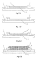
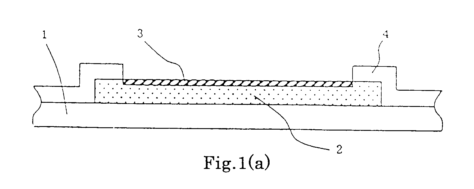
- Fig. 1(a) shows the state in which, on a semiconductor substrate 1, there is provided an Al electrode pad 2 covered with a protective film 4. Further, the protective film 4 has an opening portion in its region for forming a projected electrode; in the opening portion, the Al electrode pad 2 is exposed. On the Al electrode pad 2 in the opening portion, there exists a surface oxide film 3 which has been formed by the heat treatment step performed after the formation of the pad.
- the surface oxide film 3 is composed mainly of aluminum oxide.
- Fig. 1(b) shows the state in which the surface oxide film 3 on the Al electrode pad 2 is removed by sputtering.
- This sputtering should desirably be carried out under the condition that the output is 500 W to 1000 W, and the treating time is 5 to 30 (for example, 5 minutes).
- an inert gas such as Ar can be used as the discharging gas.
- the sputtering is carried out in a high vacuum, then the impurities in the vacuum chamber are decreased, and thus, the surface oxide film on the Al electrode pad can be removed more uniformly. As a result, a film of a first metal which will be formed later can be deposited with a more uniform and dense particle diameter.
- the sputtering output is less than 500 W, the removal of the oxide film become imperfect, so that it becomes difficult to obtain a projected electrode with a good surface shape and thus not desirable. Further, if the output exceeds 1000 W, then there arises the possibility that the active elements on the semiconductor substrate may be destroyed, which is not desirable.
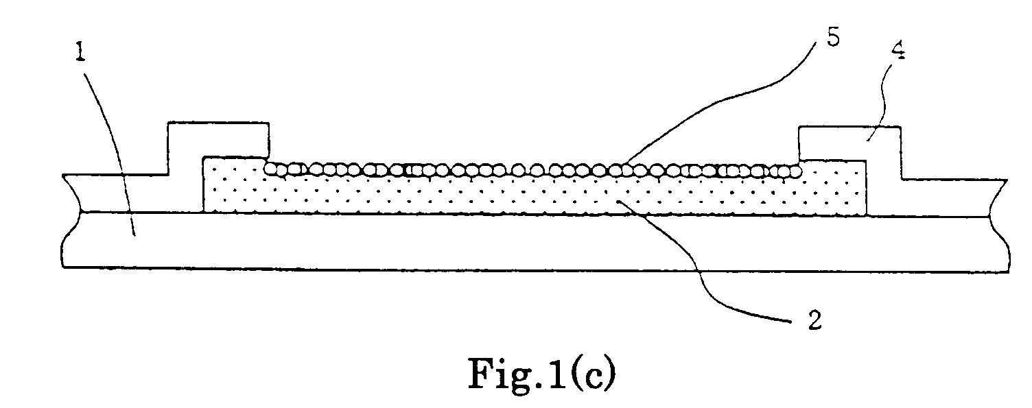
- Fig. 1(c) is a sectional view of the state in which a film of a first metal 5 is formed on the surface of the Al electrode pad 2. Since the surface oxide film 3 on the Al electrode pad 2 is already removed by sputtering, the substituting reaction between Al and the first metal is uniformly effected, in the air, on the Al electrode pad 2. According to the present invention, the film of the first metal can be densely deposited with a particle diameter of 1/10 or less, as compared with the case where the surface oxide film on the Al electrode pad 2 is removed by etching with the known solution.
- the film of the first metal is formed on the Al electrode pad by substituting reaction with Al constituting the Al electrode pad.
- a Zn film is pointed out as usable.
- the method of forming the film of the first metal there is pointed out the method according to which the Al constituting the Al electrode pad is substituted with a first metal. This method corresponds to the pre-treatment in the electroless plating method.
- the step of forming the film of the first metal in case the first metal is Zn.
- the film of the first metal is obtained by dipping the Al electrode pad in an alkaline solution containing Zn at 25 °C for about 30 seconds.
- the film of the first metal thus obtained comprises a Zn film with a thickness of 300 to 500 ⁇ .
- the Zn film is formed more uniform and dense.
- the Al electrode pad suffers a film reduction when dipped, so that, if the dipping is excessively repeated, then the Al electrode pad will be gone. As a result, the adhesion acting between the Zn film and the semiconductor substrate is lost. Accordingly, the dipping should desirably be performed about once or twice.
- the sample In case the projected electrode is formed, by the plating method, directly on the Al electrode pad 2 of which the surface oxide film has been removed by sputtering as according to the known technique, the sample must be moved from within the vacuum chamber in the sputtering system directly into an inert atmosphere. This is for preventing the formation of a surface oxide film which adversely affects the formation of the projected electrode in the air.
- the film of the first metal 5 is formed with uniformity and denseness. Therefore, surface oxide film that is formed in the air has not caused a problem.
- Fig. 1(d) shows the state in which, on the Al electrode pad 2, a projected electrode 6 comprising a film of a second metal is formed by the electroless plating method.
- the film of the second metal should desirably be composed of Ni or Ni alloy.
- the projected electrode 6 which is composed of Ni or Ni alloy should desirably be formed by dipping the sample in a solution containing Ni or both of a metal which forms an alloy with Ni and Ni at 30 to 95 °C for 2 to 200 minutes (preferably, at about 90 °C and for about 20 minutes). Since the film of the first metal is formed with uniformity and denseness, the projected electrode thus formed also becomes uniform and dense. Due to this, the surface of the projected electrode assumes a gap-less and smooth shape.
- the height of the projected electrode 6 is preferably about 0.5 ⁇ m or greater by taking into consideration the securing of the space for the semiconductor substrate and the conductor lead when the semiconductor device is connected to the conductor lead projecting into the device hole and the space for another substrate and the semiconductor substrate.
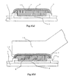
- Fig. 2(a) is a diagram showing the state in which an Au film is formed on the surface of the projected electrode 6 by the flash plating method.
- the Au film thus obtained is formed to a thickness of about 0.05 ⁇ m.
- This Au film can prevent the projected electrode from being oxidized, and the formation of this Au film is executed as a pre-treatment for the formation of an Au layer by an electroless plating step.
- the semiconductor device can be mounted onto a conductor pattern wired on an insulating film with no device hole, a general printed circuit board or glass, a ceramic substrate, etc.
- ACF anisotropic conductive film
- the temperature at this time should desirably be 200 °C, and the pressure about 1000 kg/cm 2 .
- the projected electrode 6 and the conductor pattern 9 are connected to each other through conductive particles 10.
- Fig. 3(a) is a diagram showing the state in which, on the Au film 7, an Au layer 12 is formed by electroless plating.
- the Au layer is grown by the reducing agent in the plating solution.
- the semiconductor device is connected, on an insulating film having a device hole, to a conductor lead 13 projecting into the device hole and electrically connected from a wired conductor pattern (Fig. 3(b)).
- the conductor lead 13 projecting from the device hole is plated with Sn, and, on the projected electrode 6, an Au layer 12 is formed to a thickness of 1 ⁇ m or more by electroless plating.
- the Au layer 12 and the conductor lead are positionally aligned with each other and thermo-compression-bonded together at a time.
- the thermo-compression bonding should desirably be carried out at a temperature of about 500 °C and under a pressure of about 1200 kg/cm 2 .
- the thickness of the Sn-plating layer of the conductor lead should desirably be adjusted so that the ratio between the Au and Sn in the thermo-compression-bonded portion may become about 8 (Au) : 2 (Sn) in terms of weight ratio.
- the etching of the surface oxide film on the Al electrode pad can be stably carried out, and thus, the film of the first metal can be stably formed with uniformity and denseness.
- the subsequent electroless plating can also be carried out stably, whereby the projected electrode comprising the film of the second metal can be formed with uniformity and denseness.
- the large-scale apparatus for carrying out the plating step in an inert atmosphere becomes disused.
- the film of the second metal constituting the projected electrode can also be formed with uniformity and denseness and with a minute grain size; and thus, the surface of the film of the second metal can be formed in a smooth shape.
- the film of the first metal is formed with uniformity and denseness. Further, since the film of the first metal covers the Al electrode pad, it becomes possible to carry out an electroless plating in the air at the next step, using a desired metal.
- the reliability in the connection is affected by the surface state of the projected electrode.
- the Au film can be formed even and uniform.
- the reliability in the connection is largely affected by the shape of the projected electrode and its surface state.
- the Au layer can be formed with a thickness of 1 ⁇ m or greater and with a dense surface state.
- the conductor lead and the projected electrode are connected to each other by forming an eutectic alloy of the metals which constitute the conductor lead and the projected electrode, respectively.
- connection using an ACF is made possible.
- the conductive particles in the ACF are about 3 to 5 ⁇ m in size, so that, if the projected electrode surface is coarse, then the conductive particles get afloat to make the connection unstable, causing defects such as open-circuit.
- the projected electrode with an Au layer which is constituted according to the present invention so as to have a dense surface state, highly reliable connection becomes possible.
- the projected electrode itself has a strength of bond since the substituting between Al and the first metal is effected with denseness and uniformity; and the projected electrode can also be made dense and fine in its grain size. Thus, it is possible to obtain a projected electrode which is highly resistant to the penetration of impurities from the outside and has a high reliability.
Landscapes
- Internal Circuitry In Semiconductor Integrated Circuit Devices (AREA)
- Chemically Coating (AREA)
- Electrodes Of Semiconductors (AREA)
- Wire Bonding (AREA)
Abstract

Description
Claims (9)
- A process of fabricating a semiconductor device which has a wiring layer and active elements on a semiconductor substrate, the wiring layer and the active elements being protected by a protective film, and is provided with a projected electrode for connection with a outside in an opening portion of the protective film on an Al electrode pad electrically connected to the wiring layer, which comprises the steps of:removing by sputtering a surface oxide film formed on a surface of the Al electrode pad;depositing a film of a first metal on the Al electrode pad by substituting the first metal with Al constituting the Al electrode pad; anddepositing a film of a second metal for constituting the projected electrode on the film of the first metal by substituting the first metal with the second metal, and forming the projected electrode by electroless plating by use of autocatalytic reaction.
- The fabricating process according to claim 1, wherein the sputtering is carried out at an output of 500W to 1,000W.
- The fabricating process according to claim 1, wherein the sputtering is carried out in an atmosphere of an inert gas.
- The fabricating process according to claim 1, wherein the film of the first metal is a film of Zn and the film of the second metal is a film of Ni or a Ni alloy.
- The fabricating process according to claim 4, wherein the Zn film is formed by immersing the Al electrode pad in an alkaline solution containing Zn a plurality of times.
- The fabricating process according to claim 4, wherein the Zn film has a thickness of 300Å to 500Å.
- The fabricating process according to claim 1, wherein the projected electrode has a height of 0.5 µm to 50 µm.
- A process of fabricating a semiconductor device which has an Al electrode pad and a projected electrode for external connection on the Al electrode pad, said process comprising the steps of:removing by sputtering a surface oxide film formed on a surface of the Al electrode pad;depositing a film of a first metal on the Al electrode pad by substituting the first metal with Al constituting the Al electrode pad; anddepositing a film of a second metal for constituting the projected electrode on the film of the first metal by substituting the first metal with the second metal.
- A process for forming a projected electrode on an Al electrode of a semiconductor device, wherein prior to a plurality of steps of metal film deposition by successive metal substitution, an oxide film is removed from the surface of the Al electrode by sputtering.
Applications Claiming Priority (2)
| Application Number | Priority Date | Filing Date | Title |
|---|---|---|---|
| JP03677699A JP3483490B2 (en) | 1999-02-16 | 1999-02-16 | Method for manufacturing semiconductor device |
| JP3677699 | 1999-02-16 |
Publications (2)
| Publication Number | Publication Date |
|---|---|
| EP1030356A2 true EP1030356A2 (en) | 2000-08-23 |
| EP1030356A3 EP1030356A3 (en) | 2002-11-20 |
Family
ID=12479184
Family Applications (1)
| Application Number | Title | Priority Date | Filing Date |
|---|---|---|---|
| EP00300858A Withdrawn EP1030356A3 (en) | 1999-02-16 | 2000-02-03 | Process of fabricating semiconductor device |
Country Status (5)
| Country | Link |
|---|---|
| US (1) | US6319830B1 (en) |
| EP (1) | EP1030356A3 (en) |
| JP (1) | JP3483490B2 (en) |
| KR (1) | KR100362866B1 (en) |
| TW (1) | TW436906B (en) |
Families Citing this family (13)
| Publication number | Priority date | Publication date | Assignee | Title |
|---|---|---|---|---|
| US6642136B1 (en) | 2001-09-17 | 2003-11-04 | Megic Corporation | Method of making a low fabrication cost, high performance, high reliability chip scale package |
| US6815324B2 (en) | 2001-02-15 | 2004-11-09 | Megic Corporation | Reliable metal bumps on top of I/O pads after removal of test probe marks |
| US6818545B2 (en) | 2001-03-05 | 2004-11-16 | Megic Corporation | Low fabrication cost, fine pitch and high reliability solder bump |
| TWI313507B (en) | 2002-10-25 | 2009-08-11 | Megica Corporatio | Method for assembling chips |
| US7099293B2 (en) | 2002-05-01 | 2006-08-29 | Stmicroelectronics, Inc. | Buffer-less de-skewing for symbol combination in a CDMA demodulator |
| TWI245402B (en) | 2002-01-07 | 2005-12-11 | Megic Corp | Rod soldering structure and manufacturing process thereof |
| US7470997B2 (en) * | 2003-07-23 | 2008-12-30 | Megica Corporation | Wirebond pad for semiconductor chip or wafer |
| US8067837B2 (en) * | 2004-09-20 | 2011-11-29 | Megica Corporation | Metallization structure over passivation layer for IC chip |
| US8294279B2 (en) | 2005-01-25 | 2012-10-23 | Megica Corporation | Chip package with dam bar restricting flow of underfill |
| JP4775369B2 (en) * | 2007-12-17 | 2011-09-21 | 富士電機株式会社 | Semiconductor chip, semiconductor device, and manufacturing method |
| WO2013067659A1 (en) * | 2011-11-11 | 2013-05-16 | Chu Tse-Ming | Bump structure of wafer bonding pad and manufacturing method thereof |
| JP2019029581A (en) * | 2017-08-02 | 2019-02-21 | ルネサスエレクトロニクス株式会社 | Semiconductor device manufacturing method |
| JP7027066B2 (en) | 2017-08-24 | 2022-03-01 | ルネサスエレクトロニクス株式会社 | Semiconductor devices and their manufacturing methods |
Family Cites Families (5)
| Publication number | Priority date | Publication date | Assignee | Title |
|---|---|---|---|---|
| JPH03209770A (en) * | 1990-01-11 | 1991-09-12 | Fuji Electric Co Ltd | Schottky barrier diode |
| US5938845A (en) * | 1995-10-20 | 1999-08-17 | Aiwa Co., Ltd. | Uniform heat distribution apparatus and method for electroless nickel plating in fabrication of thin film head gaps |
| JP3334489B2 (en) * | 1996-05-13 | 2002-10-15 | 松下電器産業株式会社 | Semiconductor device manufacturing method and manufacturing apparatus |
| JPH09326395A (en) * | 1996-06-06 | 1997-12-16 | Matsushita Electric Ind Co Ltd | Method for forming electrode of semiconductor device |
| JP3931454B2 (en) | 1998-11-10 | 2007-06-13 | ソニー株式会社 | Method for manufacturing electrode of semiconductor device |
-
1999
- 1999-02-16 JP JP03677699A patent/JP3483490B2/en not_active Expired - Fee Related
-
2000
- 2000-01-26 TW TW089101316A patent/TW436906B/en not_active IP Right Cessation
- 2000-02-03 EP EP00300858A patent/EP1030356A3/en not_active Withdrawn
- 2000-02-07 US US09/498,656 patent/US6319830B1/en not_active Expired - Lifetime
- 2000-02-15 KR KR1020000007044A patent/KR100362866B1/en not_active Expired - Fee Related
Also Published As
| Publication number | Publication date |
|---|---|
| TW436906B (en) | 2001-05-28 |
| JP3483490B2 (en) | 2004-01-06 |
| JP2000235964A (en) | 2000-08-29 |
| KR100362866B1 (en) | 2002-12-11 |
| KR20000058054A (en) | 2000-09-25 |
| EP1030356A3 (en) | 2002-11-20 |
| US6319830B1 (en) | 2001-11-20 |
Similar Documents
| Publication | Publication Date | Title |
|---|---|---|
| US3761309A (en) | Ctor components into housings method of producing soft solderable contacts for installing semicondu | |
| US6268619B1 (en) | Semiconductor device with high aspect ratio via hole including solder repelling coating | |
| KR910006949B1 (en) | Bump and method for bump manufactured | |
| US5907790A (en) | Aluminum-palladium alloy for initiation of electroless plating | |
| US6396148B1 (en) | Electroless metal connection structures and methods | |
| US5151168A (en) | Process for metallizing integrated circuits with electrolytically-deposited copper | |
| US5917244A (en) | Integrated circuit inductor structure formed employing copper containing conductor winding layer clad with nickel containing conductor layer | |
| US6713377B2 (en) | Method of electroless plating copper on nitride barrier | |
| US7312164B2 (en) | Selective passivation of exposed silicon | |
| US6319830B1 (en) | Process of fabricating semiconductor device | |
| US4652336A (en) | Method of producing copper platforms for integrated circuits | |
| US4816323A (en) | Multilayer wiring substrate | |
| US5620611A (en) | Method to improve uniformity and reduce excess undercuts during chemical etching in the manufacture of solder pads | |
| KR0154139B1 (en) | Copper based metallizations for hybrid integrated circuits | |
| US6787456B1 (en) | Wafer-level inter-connector formation method | |
| US5527734A (en) | Method of manufacturing a semiconductor device by forming pyramid shaped bumps using a stabilizer | |
| US6583058B1 (en) | Solid hermetic via and bump fabrication | |
| US6838009B2 (en) | Rework method for finishing metallurgy on chip carriers | |
| JP3274381B2 (en) | Method for forming bump electrode of semiconductor device | |
| US6747351B2 (en) | Semiconductor device and method of manufacturing of the same | |
| JP4520665B2 (en) | Printed wiring board, manufacturing method thereof, and component mounting structure | |
| JPH04217323A (en) | Manufacture of bump electrode for semiconductor device | |
| EP0523791A2 (en) | Method of providing a copper pattern on a dielectric substrate | |
| JPH09326395A (en) | Method for forming electrode of semiconductor device | |
| JP3242827B2 (en) | Method for manufacturing semiconductor device |
Legal Events
| Date | Code | Title | Description |
|---|---|---|---|
| PUAI | Public reference made under article 153(3) epc to a published international application that has entered the european phase |
Free format text: ORIGINAL CODE: 0009012 |
|
| AK | Designated contracting states |
Kind code of ref document: A2 Designated state(s): AT BE CH CY DE DK ES FI FR GB GR IE IT LI LU MC NL PT SE |
|
| AX | Request for extension of the european patent |
Free format text: AL;LT;LV;MK;RO;SI |
|
| PUAL | Search report despatched |
Free format text: ORIGINAL CODE: 0009013 |
|
| AK | Designated contracting states |
Kind code of ref document: A3 Designated state(s): AT BE CH CY DE DK ES FI FR GB GR IE IT LI LU MC NL PT SE |
|
| AX | Request for extension of the european patent |
Free format text: AL;LT;LV;MK;RO;SI |
|
| 17P | Request for examination filed |
Effective date: 20030128 |
|
| AKX | Designation fees paid |
Designated state(s): DE FR GB |
|
| 17Q | First examination report despatched |
Effective date: 20070103 |
|
| STAA | Information on the status of an ep patent application or granted ep patent |
Free format text: STATUS: THE APPLICATION IS DEEMED TO BE WITHDRAWN |
|
| 18D | Application deemed to be withdrawn |
Effective date: 20100928 |