EP1030222A2 - Lithographic projection apparatus - Google Patents
Lithographic projection apparatus Download PDFInfo
- Publication number
- EP1030222A2 EP1030222A2 EP00301041A EP00301041A EP1030222A2 EP 1030222 A2 EP1030222 A2 EP 1030222A2 EP 00301041 A EP00301041 A EP 00301041A EP 00301041 A EP00301041 A EP 00301041A EP 1030222 A2 EP1030222 A2 EP 1030222A2
- Authority
- EP
- European Patent Office
- Prior art keywords
- radiation
- substrate
- type
- mask
- level
- Prior art date
- Legal status (The legal status is an assumption and is not a legal conclusion. Google has not performed a legal analysis and makes no representation as to the accuracy of the status listed.)
- Granted
Links
Images
Classifications
-
- B—PERFORMING OPERATIONS; TRANSPORTING
- B82—NANOTECHNOLOGY
- B82Y—SPECIFIC USES OR APPLICATIONS OF NANOSTRUCTURES; MEASUREMENT OR ANALYSIS OF NANOSTRUCTURES; MANUFACTURE OR TREATMENT OF NANOSTRUCTURES
- B82Y10/00—Nanotechnology for information processing, storage or transmission, e.g. quantum computing or single electron logic
-
- B—PERFORMING OPERATIONS; TRANSPORTING
- B82—NANOTECHNOLOGY
- B82Y—SPECIFIC USES OR APPLICATIONS OF NANOSTRUCTURES; MEASUREMENT OR ANALYSIS OF NANOSTRUCTURES; MANUFACTURE OR TREATMENT OF NANOSTRUCTURES
- B82Y40/00—Manufacture or treatment of nanostructures
-
- G—PHYSICS
- G03—PHOTOGRAPHY; CINEMATOGRAPHY; ANALOGOUS TECHNIQUES USING WAVES OTHER THAN OPTICAL WAVES; ELECTROGRAPHY; HOLOGRAPHY
- G03F—PHOTOMECHANICAL PRODUCTION OF TEXTURED OR PATTERNED SURFACES, e.g. FOR PRINTING, FOR PROCESSING OF SEMICONDUCTOR DEVICES; MATERIALS THEREFOR; ORIGINALS THEREFOR; APPARATUS SPECIALLY ADAPTED THEREFOR
- G03F7/00—Photomechanical, e.g. photolithographic, production of textured or patterned surfaces, e.g. printing surfaces; Materials therefor, e.g. comprising photoresists; Apparatus specially adapted therefor
- G03F7/70—Microphotolithographic exposure; Apparatus therefor
- G03F7/70008—Production of exposure light, i.e. light sources
- G03F7/7005—Production of exposure light, i.e. light sources by multiple sources, e.g. light-emitting diodes [LED] or light source arrays
-
- G—PHYSICS
- G03—PHOTOGRAPHY; CINEMATOGRAPHY; ANALOGOUS TECHNIQUES USING WAVES OTHER THAN OPTICAL WAVES; ELECTROGRAPHY; HOLOGRAPHY
- G03F—PHOTOMECHANICAL PRODUCTION OF TEXTURED OR PATTERNED SURFACES, e.g. FOR PRINTING, FOR PROCESSING OF SEMICONDUCTOR DEVICES; MATERIALS THEREFOR; ORIGINALS THEREFOR; APPARATUS SPECIALLY ADAPTED THEREFOR
- G03F7/00—Photomechanical, e.g. photolithographic, production of textured or patterned surfaces, e.g. printing surfaces; Materials therefor, e.g. comprising photoresists; Apparatus specially adapted therefor
- G03F7/70—Microphotolithographic exposure; Apparatus therefor
- G03F7/70425—Imaging strategies, e.g. for increasing throughput or resolution, printing product fields larger than the image field or compensating lithography- or non-lithography errors, e.g. proximity correction, mix-and-match, stitching or double patterning
- G03F7/70466—Multiple exposures, e.g. combination of fine and coarse exposures, double patterning or multiple exposures for printing a single feature
-
- G—PHYSICS
- G03—PHOTOGRAPHY; CINEMATOGRAPHY; ANALOGOUS TECHNIQUES USING WAVES OTHER THAN OPTICAL WAVES; ELECTROGRAPHY; HOLOGRAPHY
- G03F—PHOTOMECHANICAL PRODUCTION OF TEXTURED OR PATTERNED SURFACES, e.g. FOR PRINTING, FOR PROCESSING OF SEMICONDUCTOR DEVICES; MATERIALS THEREFOR; ORIGINALS THEREFOR; APPARATUS SPECIALLY ADAPTED THEREFOR
- G03F7/00—Photomechanical, e.g. photolithographic, production of textured or patterned surfaces, e.g. printing surfaces; Materials therefor, e.g. comprising photoresists; Apparatus specially adapted therefor
- G03F7/70—Microphotolithographic exposure; Apparatus therefor
- G03F7/708—Construction of apparatus, e.g. environment aspects, hygiene aspects or materials
- G03F7/70858—Environment aspects, e.g. pressure of beam-path gas, temperature
- G03F7/70866—Environment aspects, e.g. pressure of beam-path gas, temperature of mask or workpiece
-
- H—ELECTRICITY
- H01—ELECTRIC ELEMENTS
- H01J—ELECTRIC DISCHARGE TUBES OR DISCHARGE LAMPS
- H01J37/00—Discharge tubes with provision for introducing objects or material to be exposed to the discharge, e.g. for the purpose of examination or processing thereof
- H01J37/30—Electron-beam or ion-beam tubes for localised treatment of objects
- H01J37/317—Electron-beam or ion-beam tubes for localised treatment of objects for changing properties of the objects or for applying thin layers thereon, e.g. for ion implantation
- H01J37/3174—Particle-beam lithography, e.g. electron beam lithography
-
- H—ELECTRICITY
- H01—ELECTRIC ELEMENTS
- H01J—ELECTRIC DISCHARGE TUBES OR DISCHARGE LAMPS
- H01J2237/00—Discharge tubes exposing object to beam, e.g. for analysis treatment, etching, imaging
- H01J2237/20—Positioning, supporting, modifying or maintaining the physical state of objects being observed or treated
- H01J2237/2001—Maintaining constant desired temperature
Definitions
- the invention relates to a lithographic projection apparatus comprising:
- the invention relates to such a device in which the radiation of the first type comprises particulate radiation (e.g. electrons or ions), X-rays or extreme ultra-violet radiation (EUV).
- particulate radiation e.g. electrons or ions
- EUV extreme ultra-violet radiation
- the mask may contain a circuit pattern corresponding to an individual layer of the IC, and this pattern can then be imaged onto a target area (die) on a substrate (silicon wafer) which has been coated with a layer of photosensitive material (resist).
- a single wafer will contain a whole network of adjacent dies that are successively irradiated through the reticle, one at a time.
- each die is irradiated by exposing the entire reticle pattern onto the die in one go; such an apparatus is commonly referred to as a waferstepper.
- each die is irradiated by progressively scanning the reticle pattern under the projection beam in a given reference direction (the "scanning" direction) while synchronously scanning the wafer table parallel or anti-parallel to this direction; since, in general, the projection system will have a magnification factor M (usually, M ⁇ 1), the speed ⁇ at which the wafer table is scanned will be a factor M times that at which the reticle table is scanned. More information with regard to lithographic devices as here described can be gleaned from International Patent Application WO 97/33205, for example.
- apparatus of this type contained a single mask table and a single substrate table.
- machines are now becoming available in which there are at least two independently movable substrate tables; see, for example, the multi-stage apparatus described in International Patent Applications WO 98/28665 and WO 98/40791.
- the basic operating principle behind such multi-stage apparatus is that, while a first substrate table is underneath the projection system so as to allow exposure of a first substrate located on that table, a second substrate table can run to a loading position, discharge an exposed substrate, pick up a new substrate, perform some initial alignment and/or leveling measurements on the new substrate, and then stand by to transfer this new substrate to the exposure position underneath the projection system as soon as exposure of the first substrate is completed, whence the cycle repeats itself; in this manner, it is possible to achieve a substantially increased machine throughput, which in turn improves the cost of ownership of the machine.
- the radiation of the first type is, for example, ultra-violet (UV) radiation with a wavelength of 365 or 248 nm
- its magnitude is usually not so great as to cause substantial under-performance of the apparatus.
- the radiation of the first type comprises, for example, electrons, ions, X-rays or EUV radiation (i.e . UV with a wavelength in the range 10-25 nm, e.g. 13.6 nm); in such apparatus, localized heating of the substrate can be quite intense.
- the apparatus further comprises:
- the invention ensures that those parts of the substrate which fall in the shadow of the radiation of the first type are illuminated (and consequently heated) by radiation of the second type, and vice versa ; however, appropriate choice of the photosensitive material on the substrate, and of the type (e.g. wavelength) of the radiation of the second type, will ensure that the photosensitive material will only be exposed by the first-type radiation, and not by the second-type radiation.
- Proper adjustment of the second-type radiation dose at substrate level ensures that the substrate surface is heated to a substantially uniform temperature over at least that area which is to be covered with whole dies, thereby combating differential heating effects.
- the current invention can be envisaged at different levels, thus determining the size of the "given area" referred to in the penultimate paragraph above.
- a basic level when one die (target area) on the substrate is being exposed to first-type radiation, the (whole) substrate area outside that die can be concurrently exposed to second-type radiation; this will be referred to hereunder as a “coarse-level correction”.
- the invention can be applied within a given die: the shadowed (masked) areas within that die are then irradiated with second-type radiation while the rest of the area within the die is exposed to first-type radiation; this will be referred to hereunder as a "fine-level correction". It is also possible to combine a coarse-level and fine-level correction.
- the radiation of the first type is selected from the group formed by electrons, ions, X-rays and EUV radiation.
- Lithographic systems employing such post-optical radiation are presently undergoing development and preliminary testing by several companies, in reply to the semiconductor industry's continuing drive toward smaller feature sizes, and the consequent demand for greater lithographic image resolution.
- Preliminary investigations have shown that the use of such radiation types can lead to very substantial substrate heating, with the attendant risk of producing significant differential stresses in the substrate; consequently, the present invention represents a particularly important contribution to these technologies. More information with regard to post-optical lithographic apparatus can be obtained, for example, from:
- the radiation of the second type is selected from the group formed by microwaves, infrared radiation, visible light, and ultra-violet radiation.
- the resist employed on the substrate must be substantially insensitive to the radiation of the second type.
- the employed second-type radiation must be one to which such DUV resists are insensitive, e.g. infra-red radiation, or visible light with a wavelength longer than yellow.
- control means comprise a stencil plate.
- the second-type radiation should impinge on those parts of the substrate that are in the shadow of the first-type radiation, and vice versa. This can be realized in a relatively simple manner by locating a stencil plate between the secondary radiation source and the substrate.
- such a stencil plate will comprise an obscuration which shields a shadow-area the size of a die (or, in the case of a step-and-scan device, the size of the scanning slit-image on the substrate), while allowing radiation access to the region around the shadow-area; in use, the plate will be positioned at any given moment during the wafer exposure such that the shadow-area coincides with a subject die upon which imaging is occurring (with first type radiation), whereby second-type radiation is allowed to impinge on (all) areas of the wafer except the said subject die (in the case of a step-and-scan device, the second-type radiation will be allowed to impinge on the substrate area outside the (moving) slit area).
- At least part of the stencil plate should contain a pattern which is substantially a negative of the pattern to be imaged onto each die (using first-type radiation); the term "negative" here indicates that the stencil pattern is an inverse or complimentary image of the pattern to be imaged on the die.
- control means comprise:
- the memory means can be provided in one go with a "map" of the pattern to be projected from the mask; this can be done, for example, prior to an exposure session (batch), by loading a map-file into the memory means from a map library.
- the memory means can be programmed "on the fly", using a technique whereby, instead of providing a file with prior information regarding the mask pattern, such information is instead "measured” and stored in memory.
- the control means comprise:
- the application of the current invention will alleviate the problem of differential heating of a substrate during use of a lithographic apparatus.
- the substrate will still tend to get hot as a whole, and this can also be undesired.
- Such "global" heating of the substrate is alleviated by substantial heat removal through the substrate table on which the substrate is located.
- a pattern in a mask is imaged onto a substrate which is at least partially covered by a layer of energy-sensitive material (resist).
- the substrate Prior to this imaging step, the substrate may undergo various procedures, such as priming, resist coating and a soft bake. After exposure, the substrate may be subjected to other procedures, such as a post-exposure bake (PEB), development, a hard bake and measurement/inspection of the imaged features.
- PEB post-exposure bake
- This array of procedures is used as a basis to pattern an individual layer of a device, e.g. an IC.
- Such a patterned layer may then undergo various processes such as etching, ion-implantation (doping), metallization, oxidation, chemo-mechanical polishing, etc., all intended to finish off an individual layer. If several layers are required, then the whole procedure, or a variant thereof, will have to be repeated for each new layer. Eventually, an array of devices will be present on the substrate (wafer). These devices are then separated from one another by a technique such as dicing or sawing, whence the individual devices can be mounted on a carrier, connected to pins, etc. Further information regarding such processes can be obtained, for example, from the book “Microchip Fabrication: A Practical Guide to Semiconductor Processing", Third Edition, by Peter van Zant, McGraw Hill Publishing Co., 1997, ISBN 0-07-067250-4.
- the apparatus according to the invention may be employed in the manufacture of integrated optical systems, guidance and detection patterns for magnetic domain memories, liquid-crystal display panels, thin-film magnetic heads, etc.
- any use of the terms “reticle”, “wafer” or “die” in this text should be considered as being replaced by the more general terms “mask”, "substrate” and “target area”, respectively.
- the apparatus according to the invention may, if desired, contain more than one substrate table and/or more than one mask table (so-called twin-stage or multi-stage machines).
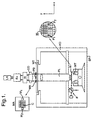
- Figure 1 schematically depicts a lithographic projection apparatus in which the current invention can be applied.
- the apparatus comprises:
- the radiation system comprises a source LA (e.g. an electron gun or ion source, a wiggler/undulator provided around the path of a charged particle beam produced by an accelerator, or a laser source) that produces a beam of radiation.
- a source LA e.g. an electron gun or ion source, a wiggler/undulator provided around the path of a charged particle beam produced by an accelerator, or a laser source
- This beam is passed along various optical components, ⁇ e.g. beam shaping optics Ex, an integrator IN and a condensor CO ⁇ so that the resultant beam PB has a desired shape and intensity distribution in its cross-section.
- the beam PB subsequently intercepts the mask MA which is held in a mask holder on a mask table MT. Having passed through (or been reflected from) the mask MA, the beam PB passes trough the projection system PL, which focuses the beam PB onto a target area C of the substrate W.
- the substrate table WT can be moved accurately, e.g. so as to position different target areas C in the path of the beam PB.
- movement of the tables MT, WT will be realized with the aid of a long stroke module (course positioning) and a short stroke module (fine positioning), which are not explicitly depicted in Figure 1.
- the mask table MT may be provided with only a short-stroke module, for fine positioning.
- the depicted apparatus can be used in two different modes:
- the plan view of the wafer W at the right of the figure shows the various die areas C into which the wafer W can be subdivided.
- these die areas C will be imaged onto one at a time.
- the subject die first-type radiation will only impinge on one particular die area C ("the subject die"), leaving the other die areas C "dark" with respect to the first-type radiation.
- the subject die C will become substantially heated through absorption of first-type radiation, whereas the surrounding dies C will remain at a lower temperature.
- This sizeable temperature difference can cause substantial stress in the wafer, resulting in local wafer expansion or even sudden slight movement of the wafer. In turn, this has a detrimental effect on the imaging performance of the lithographic apparatus.
- this problem is addressed by directing second-type radiation onto the various die areas C around the particular subject die C that is being irradiated with first-type radiation at a given moment. If the source LA is shuttered off ( e.g . during motion of the substrate table WT or during alignment and/or levelling operations prior to exposure), then the second-type radiation can, for example:
- the second-type radiation can be conveniently directed onto the wafer W using a secondary source disposed off the optical axis of the projection system PL, or by coupling the second-type radiation into the path of the first-type radiation from the source LA, for example.
- This latter method may employ a small mirror or prism, disposed near the optical axis of the projection system PL, serving to direct second-type radiation from the (laterally situated) secondary source onto a path along the optical axis and toward the substrate.
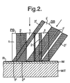
- Figure 2 is a magnified cross-section of part of the apparatus of Figure 1, after modification to render it in accordance with a particular embodiment of the present invention. As here depicted, the Figure schematically shows a fine-level correction (see above); however, the basic principle illustrated in the Figure and discussed hereunder apply also to a coarse-level correction.
- a wafer W is coated with a resist layer R and is located on top of the wafer table WT. Also depicted is part of the projection beam PB of first-type radiation, which contains "light” regions 1 and “dark” regions 2 in accordance with the pattern on the mask MA (not depicted).
- the light regions 1 give rise to exposure areas 1'' in the resist layer R, whereas the dark regions 2 give rise to non-exposure areas 2'' in the layer R; these non-exposure areas 2'' are termed as being "in the shadow" with regard to the projection beam PB.
- the projection beam also has a thermal effect on the wafer W, since the layer R and wafer W absorb energy from the beam PB and consequently become heated. As a result, the exposure areas 1'' will be heated by the projection beam PB.
- the Figure additionally depicts a secondary beam SB of second-type radiation.
- the secondary beam SB is patterned, and contains "light” regions 1' and "dark” regions 2'.
- the patterning of the secondary beam SB is such that the light regions 1' impinge upon the non-exposure areas 2'' ("shadow areas") of the resist layer R, whereas the dark regions 2' fall upon the exposure areas 1''.
- the resist R and the radiation in the secondary beam SB are chosen such that the former is not substantially exposed by the latter; consequently, the secondary beam SB has a negligible effect on the layer R as far as chemical exposure is concerned.
- the radiation in the secondary beam SB is absorbed by the layer R and the wafer W, and causes heating of the wafer W; the non-exposure areas 2'' are thus heated by the secondary beam SB.
- the intensity and nature (e.g. wavelength) of the secondary beam SB are appropriately chosen, then the temperature rise in the non-exposure regions 2'' due to beam SB will be substantially equal to the temperature rise in the exposure regions 1'' due to beam PB.
- the net effect is thus a substantially constant heating of the wafer W across its major surface, instead of the differential heating which would occur without the application of the secondary beam SB.
- the exposure regions 1'' and non-exposure regions 2'' are located within a given die. However, there will also be non-exposure regions outside that die ( viz . other dies, and intermediate strips of wafer), and these can, if desired, also be heated by a secondary beam, so as to ensure that they are kept at substantially the same temperature as the die currently being exposed.
- the depicted patterning of the secondary beam SB is such as to have been caused by the use of e.g. a stencil plate (not shown).
- the secondary beam SB can also be patterned in another manner, e.g. by scanning a single beam over the resist layer R and modulating its intensity as a function of position: a relatively high intensity is then used in the non-exposure regions 2'', and a much lower (or zero) intensity in the exposure regions 1''.
- the beam SB arrives at the substrate from an off-axis secondary source.
- the beam SB can impinge upon the substrate W in a direction substantially perpendicular to the plane of the substrate W; this can be achieved by coupling the beam SB into the beam PB using, for example, a mirror or prism arrangement.
- the beam SB itself can be derived from a lamp or laser source, and will be focused using a dedicated projection system. The skilled artisan in the field of projection lithography will know how to contrive a suitable secondary source and attendant projection system for use with a chosen second-type radiation.
- the current on/at the reticle is measured. Since the transmitted electrons or ions do not contribute to the measured current, this will be a measure of the pattern density of the reticle; in the case of a SCALPEL reticle, which in principle does not stop any electrons, a measured current difference will be the result of a difference in the generation of secondary electrons in the non-scatter regions and the high-scatter regions.
- the secondary radiation source can be adjusted as a function of the measured current.
- the secondary electron signal from the reticle is measured. Electrons or ions that do not pass through an opening in the reticle will generate secondary electrons, which can be detected. Consequently, the measured secondary electron current is a measure of the pattern density on the reticle (this also applies to SCALPEL, on the basis of the same argumentation presented in Embodiment 3).
- the secondary radiation source can be adjusted as a function of the measured secondary electron current.
- the secondary radiation source can be adjusted as a function of the measured current (direct or secondary / backscattered).
Landscapes
- Engineering & Computer Science (AREA)
- Physics & Mathematics (AREA)
- Chemical & Material Sciences (AREA)
- Nanotechnology (AREA)
- General Physics & Mathematics (AREA)
- Health & Medical Sciences (AREA)
- Crystallography & Structural Chemistry (AREA)
- Life Sciences & Earth Sciences (AREA)
- Toxicology (AREA)
- Environmental & Geological Engineering (AREA)
- Epidemiology (AREA)
- Public Health (AREA)
- Mathematical Physics (AREA)
- Theoretical Computer Science (AREA)
- Atmospheric Sciences (AREA)
- Analytical Chemistry (AREA)
- Condensed Matter Physics & Semiconductors (AREA)
- Manufacturing & Machinery (AREA)
- Exposure And Positioning Against Photoresist Photosensitive Materials (AREA)
- Exposure Of Semiconductors, Excluding Electron Or Ion Beam Exposure (AREA)
Abstract
- a radiation system LA, Ex, IN, CO for supplying a projection beam PB of radiation of a first type;
- a mask table MT for holding a mask MA;
- a substrate table WT for holding a substrate W;
- a projection system PL for imaging a portion of the mask MA, irradiated by the projection
beam PB, onto a target portion C of the substrate W,
whereby the apparatus further comprises:- a secondary source for supplying radiation SB of a second type, which can be directed onto the substrate W;
- control means for patterning the radiation SB of the second type so that it impinges on the substrate W according to a certain pattern,
Description
- a radiation system for supplying a projection beam of radiation of a first type;
- a mask table for holding a mask;
- a substrate table for holding a substrate;
- a projection system for imaging a portion of the mask, irradiated by the projection beam, onto a target potion of the substrate.
- a secondary source for supplying radiation of a second type, which can be directed onto the substrate;
- control means for patterning the radiation of the second type so that it impinges on the substrate according to a certain pattern.
- United States Patents US 5,079,112 and US 5,260,151, in the case of SCALPEL lithography employing an electron source;
- United States Patent US 5,532,496, relating to another electron-beam lithographic apparatus;
- European Patent Application EP 0 779 528 and United States Patent US 5,153,898, in the case of EUV lithography.
- the use of a radiation type such as microwave radiation or infrared radiation as a second-type radiation will generally only be appropriate in performing a coarse-level correction (see above). This is because these radiation types do not generally lend themselves to fine patterning/focusing at the resolution of the features typically present in a die;
- the successful use of the chosen second-type radiation in performing a fine-level correction (see above) will depend on the resolution of the features being imaged using the first-type radiation; if this resolution is too fine, then the (less energetic) second-type radiation will be difficult to pattern/focus at the required resolution. In this respect, performing a coarse-level correction is much easier, since, in that case, the second-type radiation need only be patterned/focused to a resolution of the order of millimeters (the width of a die) or centimeters (the width of a wafer) rather than tens of nanometers (the width of the individual IC features within a die).
- programmable memory means, for storing information regarding a pattern to be projected from the mask;
- scanning means, for scanning a radiation beam from the secondary light source over the surface of the substrate;
- attenuator means, for adjusting the intensity of the secondary light source during the said scanning motion, on the basis of the information stored in the memory means, thus causing patterned irradiation of the substrate with radiation of the second type.
- measurement means, for determining the patterned intensity distribution of radiation of the first type at a reference level between the radiation system and the substrate table;
- patterning means, for patterning the output of the secondary source so as to produce a second-type patterned intensity distribution at substrate level which is substantially a negative of the first-type patterned intensity distribution determined by the measurement means.
- the radiation of the first type comprises charged particles;
- the measurement means determine the patterned intensity distribution of the charged particles on the basis of a current measurement at the reference level.
- the measurement means determine the patterned intensity distribution of the charged particles on the basis of a secondary electron signal measurement at the reference level.
- (a) mask level;
- (b) the level of an angle-limiting aperture located in the radiation path between the mask table and the substrate table;
- (c) substrate level.
- a radiation system LA, Ex, IN, CO for supplying a projection beam PB of radiation (e.g. electrons, ions, X-rays or EUV);
- a mask table MT provided with a mask holder for holding a mask MA (e.g. a reticle);
- a substrate table WT provided with a substrate holder for holding a substrate W (e.g. a resist-coated silicon wafer);
- a projection system PL (e.g. a minor or catadioptric system, or a field lens) for imaging an irradiated portion of the mask MA onto a target portion C (die) of the substrate W.
- In step mode, the mask table MT is fixed, and an entire mask image is projected in one go (i.e. a single "flash") onto a target area C. The substrate table WT is then shifted in the X and/or Y directions so that a different target area C can be irradiated by the (stationary) beam PB;
- In scan mode, essentially the same scenario applies, except that a given target area C is not
exposed in a single "flash". Instead, the mask table MT is movable in a given direction
(the so-called "scan direction", e.g. the Y direction) with a speed ν, so that the projection
beam PB is caused to scan over a mask image; concurrently, the substrate table WT is
simultaneously moved in the same or opposite direction at a speed
- also be shuttered off, so that no second-type radiation impinges on the wafer;
- be unpatterned, so that the entire wafer face is irradiated with second-type radiation.
Claims (15)
- A lithographic projection apparatus comprising:a radiation system for supplying a projection beam of radiation of a first type;a mask table for holding a mask;a substrate table for holding a substrate;a projection system for imaging a portion of the mask, irradiated by the projection beam, onto a target portion of the substrate,
characterized in tat the apparatus further comprises:a secondary source for supplying radiation of a second type, which can be directed onto the substrate;control means for patterning the radiation of the second type so that it impinges on the substrate according to a certain pattern. - Apparatus according to Claim 1, characterized in that the radiation system is embodied to produce a first type of radiation that is selected from the group formed by electrons, ions, X-rays and extreme ultra-violet radiation.
- Apparatus according to Claim 1 or 2, characterized in that the secondary source is embodied to produce a second type of radiation which is selected from the group formed by microwaves, infrared radiation, visible light, and ultra-violet radiation.
- Apparatus according to any of the Claims 1-3, characterized in that the control means comprise a stencil plate.
- Apparatus according to any of the Claims 1-3, characterized in that the control means comprise:programmable memory means, for storing information regarding a pattern to be projected from the mask;scanning means, for scanning a radiation beam from the secondary light source over the surface of the substrate;attenuator means, for adjusting the intensity of the secondary light source during the said scanning motion, on the basis of the information stored in the memory means, thus causing patterned irradiation of the substrate with radiation of the second type.
- Apparatus according to any of the preceding Claims, characterized in that the control means comprise:measurement means, for determining the patterned intensity distribution of radiation of the first type at a reference level between the radiation system and the substrate table;patterning means, for patterning the output of the secondary source so as to produce a second-type patterned intensity distribution at substrate level which is substantially a negative of the first-type patterned intensity distribution determined by the measurement means.
- Apparatus according to Claim 6, characterized in that:the radiation of the first type comprises charged particles;the measurement means determine the patterned intensity distribution of the charged particles on the basis of a current measurement at the reference level.
- Apparatus according to Claim 6, characterized in that:the radiation of the first type comprises charged particles;the measurement means determine the patterned intensity distribution of the charged particles on the basis of a secondary electron signal measurement at the reference level.
- Apparatus according to any of the Claims 6-8, characterized in that the reference level is at mask level.
- Apparatus according to any of the Claims 6-8, characterized in that the reference level is at the level of an angle-limiting aperture located in the radiation path between the mask table and the substrate table.
- Apparatus according to any of the Claims 6-8, characterized in that the reference level is at substrate level.
- A device manufacturing method comprising the steps of:characterized in that:providing a substrate which is at least partially covered by a layer of radiation-sensitive material;providing a mask which contains a pattern;using a projection beam of radiation of a first type to project an image of at least a part of the mask pattern onto a target area of the layer of radiation-sensitive material, using a projection system,
using a secondary radiation source and associated control means, radiation of a second type is directed onto the substrate according to a certain pattern, such that the sum of the fluxes of the radiations of the first and second type at substrate level causes an elevation of the substrate temperature which is substantially constant across at least a given area of the substrate. - A method according to Claim 12, characterized in that the said given area is substantially the whole major surface of the substrate facing the projection system.
- A method according to Claim 12, characterized in that the said given area is the said target area.
- A device manufactured using a method as claimed in any of the Claims 12-14.
Priority Applications (1)
| Application Number | Priority Date | Filing Date | Title |
|---|---|---|---|
| EP00301041A EP1030222B1 (en) | 1999-02-18 | 2000-02-09 | Lithographic projection apparatus |
Applications Claiming Priority (3)
| Application Number | Priority Date | Filing Date | Title |
|---|---|---|---|
| EP99200462 | 1999-02-18 | ||
| EP99200462 | 1999-02-18 | ||
| EP00301041A EP1030222B1 (en) | 1999-02-18 | 2000-02-09 | Lithographic projection apparatus |
Publications (3)
| Publication Number | Publication Date |
|---|---|
| EP1030222A2 true EP1030222A2 (en) | 2000-08-23 |
| EP1030222A3 EP1030222A3 (en) | 2003-01-02 |
| EP1030222B1 EP1030222B1 (en) | 2006-01-04 |
Family
ID=26073002
Family Applications (1)
| Application Number | Title | Priority Date | Filing Date |
|---|---|---|---|
| EP00301041A Expired - Lifetime EP1030222B1 (en) | 1999-02-18 | 2000-02-09 | Lithographic projection apparatus |
Country Status (1)
| Country | Link |
|---|---|
| EP (1) | EP1030222B1 (en) |
Cited By (2)
| Publication number | Priority date | Publication date | Assignee | Title |
|---|---|---|---|---|
| DE10317662A1 (en) * | 2003-04-17 | 2004-11-18 | Carl Zeiss Smt Ag | Projection objective, microlithographic projection exposure system and method for producing a semiconductor circuit |
| WO2020126389A1 (en) * | 2018-12-19 | 2020-06-25 | Asml Netherlands B.V. | Lithographic apparatus with thermal conditioning system for conditioning the wafer |
Families Citing this family (1)
| Publication number | Priority date | Publication date | Assignee | Title |
|---|---|---|---|---|
| US10108096B2 (en) | 2015-08-31 | 2018-10-23 | Lithoptek LLC | Apparatus and method for using scanning light beam for film or surface modification |
Family Cites Families (6)
| Publication number | Priority date | Publication date | Assignee | Title |
|---|---|---|---|---|
| JPS60223122A (en) * | 1984-04-19 | 1985-11-07 | Canon Inc | Projection exposure device |
| JP2658051B2 (en) * | 1987-05-15 | 1997-09-30 | 株式会社ニコン | Positioning apparatus, projection exposure apparatus and projection exposure method using the apparatus |
| JP2704001B2 (en) * | 1989-07-18 | 1998-01-26 | キヤノン株式会社 | Position detection device |
| EP0823662A2 (en) * | 1996-08-07 | 1998-02-11 | Nikon Corporation | Projection exposure apparatus |
| EP0841681A3 (en) * | 1996-11-07 | 1999-05-12 | Nikon Corporation | Exposure apparatus and exposure method |
| JP3892565B2 (en) * | 1997-02-28 | 2007-03-14 | 株式会社東芝 | Pattern formation method |
-
2000
- 2000-02-09 EP EP00301041A patent/EP1030222B1/en not_active Expired - Lifetime
Cited By (4)
| Publication number | Priority date | Publication date | Assignee | Title |
|---|---|---|---|---|
| DE10317662A1 (en) * | 2003-04-17 | 2004-11-18 | Carl Zeiss Smt Ag | Projection objective, microlithographic projection exposure system and method for producing a semiconductor circuit |
| WO2004092843A3 (en) * | 2003-04-17 | 2005-03-31 | Zeiss Carl Smt Ag | Projection lens, microlithographic projection exposure system and method for producing a semiconductor circuit |
| WO2020126389A1 (en) * | 2018-12-19 | 2020-06-25 | Asml Netherlands B.V. | Lithographic apparatus with thermal conditioning system for conditioning the wafer |
| CN113330369A (en) * | 2018-12-19 | 2021-08-31 | Asml荷兰有限公司 | Lithographic apparatus with thermal conditioning system for conditioning a wafer |
Also Published As
| Publication number | Publication date |
|---|---|
| EP1030222B1 (en) | 2006-01-04 |
| EP1030222A3 (en) | 2003-01-02 |
Similar Documents
| Publication | Publication Date | Title |
|---|---|---|
| KR100583694B1 (en) | Substrate provided with an Alignment Mark, Method of Designing a Mask, Computer Program, Mask for Exposing said Mark, Device Manufacturing Method, and Device Manufactured Thereby | |
| CN100480862C (en) | Method of measurement, method for providing alignment marks, and device manufacturing method | |
| US6646274B1 (en) | Lithographic projection apparatus | |
| JP2002141280A (en) | Flat projector, manufacturing method for element and element manufactured thereby | |
| KR100547438B1 (en) | Lithographic apparatus and device manufacturing method | |
| JP4955028B2 (en) | Device manufacturing method, lithographic apparatus, and device manufactured thereby | |
| JP4058405B2 (en) | Device manufacturing method and device manufactured by this method | |
| KR20010006764A (en) | Illumination system for extreme ultraviolet radiation and its application in lithographic projection apparatus | |
| JP5060464B2 (en) | Device manufacturing method | |
| KR20020012140A (en) | Lithographic apparatus, device manufacturing method, and device manufactured thereby | |
| KR100539667B1 (en) | Lithographic projection apparatus and method of manufacturing a device and the device manufactured by the method | |
| JP4924421B2 (en) | Sensor calibration method, exposure method, exposure apparatus, device manufacturing method, and reflective mask | |
| US7081945B2 (en) | Device manufacturing method, device manufactured thereby and lithographic apparatus therefor | |
| KR100554247B1 (en) | Lithographic Apparatus, Device Manufacturing Method, and Device Manufactured Thereby | |
| JP2001244194A (en) | Abbe arm correction system used in lithography system | |
| JP2003037059A (en) | Exposure method, device manufacturing method, and lithographic projection apparatus | |
| US6870603B2 (en) | Lithographic apparatus and method to determine beam characteristics | |
| US6573977B1 (en) | Exposure control method, exposure apparatus and device manufacturing method | |
| TWI437379B (en) | Lighting system and lithography device | |
| EP1030222B1 (en) | Lithographic projection apparatus | |
| JP3583774B2 (en) | Lithographic apparatus and device manufacturing method | |
| JP2006191046A (en) | Method and exposure equipment for performing inclined focusing, and device manufactured according to the same | |
| US7113255B2 (en) | Grating patch arrangement, lithographic apparatus, method of testing, device manufacturing method, and device manufactured thereby | |
| US20090262328A1 (en) | Illumination system and lithographic method | |
| KR100554259B1 (en) | Lithographic projection apparatus and device manufacturing method |
Legal Events
| Date | Code | Title | Description |
|---|---|---|---|
| PUAI | Public reference made under article 153(3) epc to a published international application that has entered the european phase |
Free format text: ORIGINAL CODE: 0009012 |
|
| AK | Designated contracting states |
Kind code of ref document: A2 Designated state(s): AT BE CH CY DE DK ES FI FR GB GR IE IT LI LU MC NL PT SE |
|
| AX | Request for extension of the european patent |
Free format text: AL;LT;LV;MK;RO;SI |
|
| RAP1 | Party data changed (applicant data changed or rights of an application transferred) |
Owner name: ASML NETHERLANDS B.V. |
|
| PUAL | Search report despatched |
Free format text: ORIGINAL CODE: 0009013 |
|
| AK | Designated contracting states |
Kind code of ref document: A3 Designated state(s): AT BE CH CY DE DK ES FI FR GB GR IE IT LI LU MC NL PT SE |
|
| AX | Request for extension of the european patent |
Free format text: AL;LT;LV;MK;RO;SI |
|
| 17P | Request for examination filed |
Effective date: 20030625 |
|
| AKX | Designation fees paid |
Designated state(s): DE FR GB IT NL |
|
| 17Q | First examination report despatched |
Effective date: 20040623 |
|
| RAP1 | Party data changed (applicant data changed or rights of an application transferred) |
Owner name: ASML NETHERLANDS B.V. |
|
| GRAP | Despatch of communication of intention to grant a patent |
Free format text: ORIGINAL CODE: EPIDOSNIGR1 |
|
| GRAS | Grant fee paid |
Free format text: ORIGINAL CODE: EPIDOSNIGR3 |
|
| GRAA | (expected) grant |
Free format text: ORIGINAL CODE: 0009210 |
|
| AK | Designated contracting states |
Kind code of ref document: B1 Designated state(s): DE FR GB IT NL |
|
| REG | Reference to a national code |
Ref country code: GB Ref legal event code: FG4D |
|
| REF | Corresponds to: |
Ref document number: 60025303 Country of ref document: DE Date of ref document: 20060330 Kind code of ref document: P |
|
| ET | Fr: translation filed | ||
| PLBE | No opposition filed within time limit |
Free format text: ORIGINAL CODE: 0009261 |
|
| STAA | Information on the status of an ep patent application or granted ep patent |
Free format text: STATUS: NO OPPOSITION FILED WITHIN TIME LIMIT |
|
| 26N | No opposition filed |
Effective date: 20061005 |
|
| PGFP | Annual fee paid to national office [announced via postgrant information from national office to epo] |
Ref country code: GB Payment date: 20080220 Year of fee payment: 9 Ref country code: IT Payment date: 20080223 Year of fee payment: 9 Ref country code: NL Payment date: 20080214 Year of fee payment: 9 |
|
| PGFP | Annual fee paid to national office [announced via postgrant information from national office to epo] |
Ref country code: DE Payment date: 20090219 Year of fee payment: 10 |
|
| GBPC | Gb: european patent ceased through non-payment of renewal fee |
Effective date: 20090209 |
|
| PGFP | Annual fee paid to national office [announced via postgrant information from national office to epo] |
Ref country code: FR Payment date: 20090213 Year of fee payment: 10 |
|
| NLV4 | Nl: lapsed or anulled due to non-payment of the annual fee |
Effective date: 20090901 |
|
| PG25 | Lapsed in a contracting state [announced via postgrant information from national office to epo] |
Ref country code: NL Free format text: LAPSE BECAUSE OF NON-PAYMENT OF DUE FEES Effective date: 20090901 |
|
| PG25 | Lapsed in a contracting state [announced via postgrant information from national office to epo] |
Ref country code: GB Free format text: LAPSE BECAUSE OF NON-PAYMENT OF DUE FEES Effective date: 20090209 |
|
| REG | Reference to a national code |
Ref country code: FR Ref legal event code: ST Effective date: 20101029 |
|
| PG25 | Lapsed in a contracting state [announced via postgrant information from national office to epo] |
Ref country code: FR Free format text: LAPSE BECAUSE OF NON-PAYMENT OF DUE FEES Effective date: 20100301 |
|
| PG25 | Lapsed in a contracting state [announced via postgrant information from national office to epo] |
Ref country code: DE Free format text: LAPSE BECAUSE OF NON-PAYMENT OF DUE FEES Effective date: 20100901 |
|
| PG25 | Lapsed in a contracting state [announced via postgrant information from national office to epo] |
Ref country code: IT Free format text: LAPSE BECAUSE OF NON-PAYMENT OF DUE FEES Effective date: 20090209 |