EP1028562A2 - Recovery of timing in multicarrier systems - Google Patents
Recovery of timing in multicarrier systems Download PDFInfo
- Publication number
- EP1028562A2 EP1028562A2 EP00200488A EP00200488A EP1028562A2 EP 1028562 A2 EP1028562 A2 EP 1028562A2 EP 00200488 A EP00200488 A EP 00200488A EP 00200488 A EP00200488 A EP 00200488A EP 1028562 A2 EP1028562 A2 EP 1028562A2
- Authority
- EP
- European Patent Office
- Prior art keywords
- circuit
- signal
- estimate
- timing
- receiver
- Prior art date
- Legal status (The legal status is an assumption and is not a legal conclusion. Google has not performed a legal analysis and makes no representation as to the accuracy of the status listed.)
- Granted
Links
Images
Classifications
-
- H—ELECTRICITY
- H04—ELECTRIC COMMUNICATION TECHNIQUE
- H04L—TRANSMISSION OF DIGITAL INFORMATION, e.g. TELEGRAPHIC COMMUNICATION
- H04L27/00—Modulated-carrier systems
- H04L27/26—Systems using multi-frequency codes
- H04L27/2601—Multicarrier modulation systems
- H04L27/2647—Arrangements specific to the receiver only
- H04L27/2655—Synchronisation arrangements
- H04L27/2662—Symbol synchronisation
-
- H—ELECTRICITY
- H04—ELECTRIC COMMUNICATION TECHNIQUE
- H04L—TRANSMISSION OF DIGITAL INFORMATION, e.g. TELEGRAPHIC COMMUNICATION
- H04L25/00—Baseband systems
- H04L25/02—Details ; arrangements for supplying electrical power along data transmission lines
- H04L25/0202—Channel estimation
- H04L25/024—Channel estimation channel estimation algorithms
- H04L25/025—Channel estimation channel estimation algorithms using least-mean-square [LMS] method
-
- H—ELECTRICITY
- H04—ELECTRIC COMMUNICATION TECHNIQUE
- H04L—TRANSMISSION OF DIGITAL INFORMATION, e.g. TELEGRAPHIC COMMUNICATION
- H04L27/00—Modulated-carrier systems
- H04L27/26—Systems using multi-frequency codes
- H04L27/2601—Multicarrier modulation systems
- H04L27/2647—Arrangements specific to the receiver only
- H04L27/2655—Synchronisation arrangements
- H04L27/2657—Carrier synchronisation
-
- H—ELECTRICITY
- H04—ELECTRIC COMMUNICATION TECHNIQUE
- H04L—TRANSMISSION OF DIGITAL INFORMATION, e.g. TELEGRAPHIC COMMUNICATION
- H04L27/00—Modulated-carrier systems
- H04L27/26—Systems using multi-frequency codes
- H04L27/2601—Multicarrier modulation systems
- H04L27/2647—Arrangements specific to the receiver only
- H04L27/2655—Synchronisation arrangements
- H04L27/2668—Details of algorithms
- H04L27/2673—Details of algorithms characterised by synchronisation parameters
- H04L27/2676—Blind, i.e. without using known symbols
- H04L27/2679—Decision-aided
-
- H—ELECTRICITY
- H04—ELECTRIC COMMUNICATION TECHNIQUE
- H04L—TRANSMISSION OF DIGITAL INFORMATION, e.g. TELEGRAPHIC COMMUNICATION
- H04L27/00—Modulated-carrier systems
- H04L27/26—Systems using multi-frequency codes
- H04L27/2601—Multicarrier modulation systems
- H04L27/2647—Arrangements specific to the receiver only
- H04L27/2655—Synchronisation arrangements
- H04L27/2689—Link with other circuits, i.e. special connections between synchronisation arrangements and other circuits for achieving synchronisation
- H04L27/2695—Link with other circuits, i.e. special connections between synchronisation arrangements and other circuits for achieving synchronisation with channel estimation, e.g. determination of delay spread, derivative or peak tracking
Definitions
- the present application relates generally to the technical field of digital communication systems and more particularly to a method and apparatus for riming recovery in multi-carrier modulation in such a digital communication system.
- Receivers in digital communication systems are usually operable to estimate and track the phase of a clock that generates a transmit signal, so that the receiver sampling is synchronous with the transmit signal. Better efficiency (in terms of channel bandwidth) is obtained when the receiver can extract this timing phase from the information-bearing signal.
- multi-carrier modulation See “A Multicarrier Primer", ANSI T1E1.4/91-157, John M. Cioffi, November, 1991, herein incorporated by reference and, hereinafter referred to as "Cioffi"
- the information is transferred over a number of subchannels, typically 64-1024.
- a specific subchannel called a pilot
- the pilot is reserved for this purpose only, however in others the pilot is also used to transfer information.
- VDSL Very High Rate Digital Subscriber Line
- UDP unshielded twisted pair
- ADSL Asymmetric Digital Subscriber Line
- AM radio AM radio
- multi-carrier modulation is a flexible and adaptable method for use in this environment because the modulation scheme adapts to the specific signal, noise and interference conditions present at the time the connection is made.
- the choice of pilot subchannel must be made carefully because if strong interference is encountered in this subchannel, further communication may be impossible.
- Timing recovery involves two parts. During the initialization process, the characteristics of the channel, noise and interference are not known, however the signals transmitted are arranged in advance. Using these prearranged signals, the receiver must learn the timing phase and frequency of the transmitter. This is known as acquisition.
- the receiver can use supplementary information to maintain phase lock - this is known as tracking.
- the method and apparatus disclosed by the present application extract timing phase from signals received over multiple subchannels using a technique that weighs them according to the signal quality at that frequency. Further, the method and apparatus may obviate the nomination of a pilot sub-channel and preferably require no negotiation process.
- An acquisition signal (1 symbol) is transmitted repeatedly.
- the exact signal need not be known at the receiver, although it is preferred that it is uniform p.s.d. over the signal band being used. The only requirement is that it is repeated.
- An estimate of frequency error is derived from the received signal. This estimate is used to adjust a Numerically Controlled Oscillator at the receiver, which in turn determines the sampling phase.
- timing phase is maintained by using the received signal, together with estimates of the transmitted signal to develop an estimate of the phase error. This information is used to adjust a Numerically Controlled Oscillator at the receiver, which in turn determines the sampling phase.
- sampling frequency error is ⁇ f
- the effect of sampling instant shift is predicted by the time-shift theorem of Fourier Theory (see "The Fourier Transform and its Applications,” R.N. Bracewell, 2 nd Ed., McGraw-Hill, 1965, herein incorporated by reference).
- Time shift ⁇ causes phase rotation in the frequency domain 2 ⁇ f.
- each of these estimates will have the same expected value, but their variances will vary widely due to the underlying channel attenuation variation with frequency. It seems reasonable to form a weighted sum of these estimates, in which the weights w n are proportional to the signal to noise ratio in the channel.
- the channel signal-to-noise ratio SNR
- the transmitted signal is computed with certain subcarriers not used (turned “OFF"), the energy detected at the receiver in those subcarriers represents noise and interference.
- the SNR may be estimated by computing the ratio between these unused subcarriers and neighboring frequencies.
- Timing recovery/frequency error estimation usually involves computation of the angle between two complex numbers (vectors).
- vectors In acquisition, we force the data symbol to be repeated, and we measure the angle between successive symbols and attribute that o sampling frequency offset.
- the problem in tracking mode is that the data symbol X k is unknown, and is different each symbol-time.
- SNR Signal to Noise Ratio
- a phase rotation between Y k (n) and U k (n) will be due to sampling phase error, or from errors in the estimates H ⁇ or X ⁇ k . If we assume that these estimation errors are insignificant - the channel estimate is good enough, and symbol decision errors are infrequent - then the expectation of the angle between Y k (n) and U k (n) will represent the phase error, and we can use an estimate of it to drive the tracking phase-lock loop.
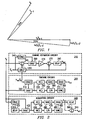
- FIG. 2 shows a preferred embodiment of a timing recovery system 200 in accordance with the present invention.
- the timing recovery system 200 in Fig. 2 includes a channel estimation circuitry 210, tracking circuitry 300, and acquisition circuitry 400.
- the channel estimation circuitry 210 accepts as input received symbol Y k and transmitted signal estimate X ⁇ k .
- Transmitted signal estimate X ⁇ k is input into conjugate circuit 240 and complex multiplier circuit 250.
- the output of the complex multiplier circuit 250 is summed with the received symbol Y k at summer 245 and input into complex multiplier circuit 260 along with the output of conjugate circuit 240.
- the output of the complex multiplier circuit 260 in then scaled by an adaptive update gain, ⁇ , at scaler circuit 270.
- the output of scaler circuit 270 is then summed at summer 280 with delayed channel estimate H est .
- the delayed channel estimate H est is the delayed output of summer 280.
- the delayed channel estimate H est is also input into complex multiplier circuit 250 and multiplied with the transmitted signal estimate X ⁇ k which, during a tracking phase of the timing recovery system 200, is input into conjugate circuit 310.
- the output of the conjugate circuit 310 is then input, along with the received symbol Y k , into complex multiplier circuit 300.
- the real portion of the output of the complex multiplier circuit 320 is then generated at circuit 330 and provided as input to summer 350.
- the imaginary portion of the output of the complex multiplier circuit 320 is generated at circuit 340 and then input into the divide-by-n circuit 360.
- the output of the divide-by-n circuit is input into summer 380.
- the outputs of summer 350 and summer 380 are then input into divide circuit 370.
- the output of divide circuit 370 is an estimated timing phase ⁇ t
- the received symbol Y k is input into conjugate circuit 410.
- the output of the conjugate circuit 410 input into delay circuit 420.
- the delayed output of delay circuit 420 in multiplied in complex multiplier circuit 430 with the received symbol Y k .
- the real portion of the output of the complex multiplier circuit 430 is generated by circuit 440 and provided as input to summer circuit 460.
- the imaginary portion of the output of the complex multiplier circuit 430 is generated by circuit 450 and then input into the divide-by-n circuit 470.
- the output of the divide-by-n circuit 470 is input into summer circuit 490.
- the outputs of summer circuits 480 and 490 are then input into divide circuit 480.
- the output of divide circuit 480 is an estimated error ⁇ a,k which is input into delay circuit 500 and summation 510.
- a delayed version of the estimated error signal ⁇ a,k is output from the delay circuit 500 and is also provided as input into summation 510.
- the sum of the error signal ⁇ a,k output from the divide circuit 480 and the delayed error signal output from the delay circuit 500 generates timing phase ⁇ a,k for use by the timing recovery system 200 during acquisition mode.
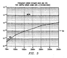
- Fig. 3 shows a graph illustrating frequency error estimate mean and standard deviation for one embodiment of a timing recovery system according to the present teachings.
Abstract
Description
- The present application relates generally to the technical field of digital communication systems and more particularly to a method and apparatus for riming recovery in multi-carrier modulation in such a digital communication system.
- Receivers in digital communication systems are usually operable to estimate and track the phase of a clock that generates a transmit signal, so that the receiver sampling is synchronous with the transmit signal. Better efficiency (in terms of channel bandwidth) is obtained when the receiver can extract this timing phase from the information-bearing signal. If multi-carrier modulation (See "A Multicarrier Primer", ANSI T1E1.4/91-157, John M. Cioffi, November, 1991, herein incorporated by reference and, hereinafter referred to as "Cioffi") is used, the information is transferred over a number of subchannels, typically 64-1024. Usually a specific subchannel, called a pilot, is designated for the transfer of timing phase. In some digital communication systems the pilot is reserved for this purpose only, however in others the pilot is also used to transfer information.
- These types of communication systems are designed to withstand random noise and interference from other communication systems. The nature of the interference, however, may not be well known. In particular, Very High Rate Digital Subscriber Line (VDSL) (See "Very-high-speed Digital Subscriber Lines", Systems Requirements Document (T1E1.4/98-043R3), American National Standards Institute, herein incorporated by reference operating in unshielded twisted pair (UTP) cable with aerial drop wires is susceptible to interference from Asymmetric Digital Subscriber Line (ADSL), amateur radio and broadcast AM radio. The frequency and strength of the interference is not known in a particular installation. Generally, multi-carrier modulation is a flexible and adaptable method for use in this environment because the modulation scheme adapts to the specific signal, noise and interference conditions present at the time the connection is made. However the choice of pilot subchannel must be made carefully because if strong interference is encountered in this subchannel, further communication may be impossible.
- An improvement would be to negotiate the pilot subchannel during the initialization process (See U.S. provisional patent application 60/078,549 entitled "Initializing Communication in Systems using Multi-carrier Modulation", herein incorporated by reference. However this method is difficult because (i) knowledge of signal and interference strengths is needed and if phase lock has not been achieved this might be inconvenient or complicated, and (ii) the negotiation process requires reliable communication between two devices which have not yet phase locked. Solving these problems may be complicated, unreliable or take excessive time.
- The extraction of timing phase information (timing recovery) involves two parts. During the initialization process, the characteristics of the channel, noise and interference are not known, however the signals transmitted are arranged in advance. Using these prearranged signals, the receiver must learn the timing phase and frequency of the transmitter. This is known as acquisition.
- Once a connection has been established and the channel, noise and interference have been measured, now the signal that is received contains unknown information, upon which decisions are made. The receiver can use supplementary information to maintain phase lock - this is known as tracking.
- The method and apparatus disclosed by the present application extract timing phase from signals received over multiple subchannels using a technique that weighs them according to the signal quality at that frequency. Further, the method and apparatus may obviate the nomination of a pilot sub-channel and preferably require no negotiation process.
- The present invention will now be further described by way of example, with reference to the accompanying drawings in which:
- Fig. 1 shows a graph illustrating an exemplary angle of approximation;
- Fig. 2 depicts a block diagram of an acquisition and tracking system; and
- Fig. 3 shows a graph exemplifying frequency error estimate using the acquisition and tracking system.
-
- An acquisition signal (1 symbol) is transmitted repeatedly. The exact signal need not be known at the receiver, although it is preferred that it is uniform p.s.d. over the signal band being used. The only requirement is that it is repeated. An estimate of frequency error is derived from the received signal. This estimate is used to adjust a Numerically Controlled Oscillator at the receiver, which in turn determines the sampling phase.
- In tracking mode, timing phase is maintained by using the received signal, together with estimates of the transmitted signal to develop an estimate of the phase error. This information is used to adjust a Numerically Controlled Oscillator at the receiver, which in turn determines the sampling phase.
- Consider a multi-carrier modulation scheme (see Cioffi) with N/2 carriers, sampling rate fs, and prefix length p. Each transmitted symbol Xk is made up of N/2 complex variables, and in time domain has time-durationThe n-th subcarrier has frequency
 If a sequence of these symbols is transmitted over a channel with transfer function H(f), the output from the channel will be

- Denote combined noise and interference by v ∼ k (n), then the received symbol is given by
- If the sampling frequency error is Δf, the sampling instant will shift in time by Δf/
f 2 / s each sample, (N +p) Δf/f 2 / s each symbol or for the k-th symbol - Since the noise and interference are not materially affected by the phase rotation we will redefine
- Similar to the development of orthogonal frequency divisional multiplexing (OFDM) frequency offset correction (see "A Technique for Orthogonal Frequency Division Multiplexing Frequency Offset Correction", Paul H. Moose, IEEE Transactions on Communications, Vol. 42, No. 10, October 1994, herein incorporated by reference, hereinafter referred to as "Moose") we will estimate ε given observations of Yk(n), with the important differences that in this case, the phase rotation caused by the frequency error is proportional to the subchannel frequency index n, and the attenuation of the channel H(f), varies substantially over the frequency band of interest. (These differences arise because the OFDM frequency offset correction algorithm disclosed by Moose was developed for an approximately flat, passband channel). Accordingly we arrive at an estimate of ε for each subchannel (see Equation A.17 of Moose, noting that the notation is changed slightly).
z denotes the complex conjugate of z, and ε ∧ κ ( n ) represents the estimate of frequency error at the k-th symbol, in the n-th subcarrier. Figure 1 shows a graph illustrating the angle approximation. - Next we will make the approximation that tan (2πnε k (n)) ≈2πnε k ( n ). This we justify by pointing out that in the VDSL application (or any non-mobile application where crystals are used), we expect frequency error ε of no more than 100 ppm (10-4), and with 256 subcarriers 2πnε<0.1608. Further, we intend to close a phase-lock-loop around this frequency error estimate, so if the loop is in lock the error will be small. Comparing with the exact form
- Now we can write
- Each of these estimates will have the same expected value, but their variances will vary widely due to the underlying channel attenuation variation with frequency. It seems reasonable to form a weighted sum of these estimates, in which the weights wn are proportional to the signal to noise ratio in the channel. However, when this algorithm is being used, namely during acquisition, the channel signal-to-noise ratio (SNR) is not known. However if the transmitted signal is computed with certain subcarriers not used (turned "OFF"), the energy detected at the receiver in those subcarriers represents noise and interference. If we presume that the channel attenuation varies smoothly with frequency, the SNR may be estimated by computing the ratio between these unused subcarriers and neighboring frequencies.
- Another (simpler) method is to assume that the noise and interference together are uniformly distributed over frequency (white noise approximation). We know that this will be false in many situations, however when averaged over all subcarriers the effect is probably small. If we make the further stipulation that the acquisition signal Xa (n) be uniform across the signal band, a measurement of received power spectral density (p.s.d.) will then provide an estimate of signal to noise ratio. This amounts to weights

- Since we have to estimate the expectation during the acquisition process, we will need to derive this from observations of Yk(n). If the acquisition signal Xa(n) is formed from PSK symbols (amplitude independent of data) then the receiver need not know Xa(n) to estimate E[|Yn (n)|2], it just needs to measure |Yk (n)|2.
- Note thatthe frequency error estimate becomes
 this can be integrated to estimate phase error using the recursion
- In the equations above, we have taken the sum over all subcarriers. However a simplication of the algorithm could be obtained by picking a subset of the subcarriers based on a compromise between computational complexity, channel quality and phase lock loop performance. For example the subset could be chosen based on knowledge that those subcarriers are not in Ham operator or AM radio bands; or only those subcarriers with SNR greater than some threshold. Denote this subset by a set of integers A each member of which represents the index, of a desired subchannel. Then each sum above becomes

- After the initial acquisition transient, the error will be small. If the acquisition signal is either arranged in advance or decisions are made assuming a known constellation (for example 4-PSK) the acquisition symbol Xa will be known at the receiver. Then the channel can be estimated recursively
- Alternatively, the LMS algorithm can be used
- Timing recovery/frequency error estimation usually involves computation of the angle between two complex numbers (vectors). In acquisition, we force the data symbol to be repeated, and we measure the angle between successive symbols and attribute that o sampling frequency offset. The problem in tracking mode is that the data symbol Xk is unknown, and is different each symbol-time. However if there is enough SNR to transfer data reliably (Pr{symbol error}<le-4?) then we can use data decisions at the receiver - estimates of Xk - to form a reference vector with which to compare the received signal vector.
- The data decisions X ∧k are multiplied by the channel estimate that was derived during acquisition H ∧(n) to form an estimate of the noiseless channel output
- A phase rotation between Yk(n) and Uk(n) will be due to sampling phase error, or from errors in the estimates H ∧ or X ∧k . If we assume that these estimation errors are insignificant - the channel estimate is good enough, and symbol decision errors are infrequent - then the expectation of the angle between Yk(n) and Uk(n) will represent the phase error, and we can use an estimate of it to drive the tracking phase-lock loop.
-
- We use the same idea as for acquisition, namely to assume that the angle is small, and weight the subcarrier estimates according to the received channel output, except that now we have phase error estimate

- Figure 2 shows a preferred embodiment of a timing recovery system 200 in accordance with the present invention. The timing recovery system 200 in Fig. 2 includes a
channel estimation circuitry 210, trackingcircuitry 300, andacquisition circuitry 400. Thechannel estimation circuitry 210 accepts as input received symbol Yk and transmitted signal estimate X ∧k . Transmitted signal estimate X ∧k is input intoconjugate circuit 240 andcomplex multiplier circuit 250. The output of thecomplex multiplier circuit 250 is summed with the received symbol Yk atsummer 245 and input into complex multiplier circuit 260 along with the output ofconjugate circuit 240. The output of the complex multiplier circuit 260 in then scaled by an adaptive update gain, µ, at scaler circuit 270. The output of scaler circuit 270 is then summed at summer 280 with delayed channel estimate Hest. The delayed channel estimate Hest is the delayed output of summer 280. The delayed channel estimate Hest is also input intocomplex multiplier circuit 250 and multiplied with the transmitted signal estimate X ∧k which, during a tracking phase of the timing recovery system 200, is input intoconjugate circuit 310. The output of theconjugate circuit 310 is then input, along with the received symbol Yk, intocomplex multiplier circuit 300. The real portion of the output of thecomplex multiplier circuit 320 is then generated atcircuit 330 and provided as input tosummer 350. The imaginary portion of the output of thecomplex multiplier circuit 320 is generated atcircuit 340 and then input into the divide-by-n circuit 360. The output of the divide-by-n circuit is input intosummer 380. The outputs ofsummer 350 andsummer 380 are then input intodivide circuit 370. The output ofdivide circuit 370 is an estimated timing phase Φt,k for use during tracking mode. - In the
acquisition circuit 400, the received symbol Yk is input intoconjugate circuit 410. The output of theconjugate circuit 410 input intodelay circuit 420. The delayed output ofdelay circuit 420 in multiplied in complex multiplier circuit 430 with the received symbol Yk. The real portion of the output of the complex multiplier circuit 430 is generated bycircuit 440 and provided as input tosummer circuit 460. The imaginary portion of the output of the complex multiplier circuit 430 is generated bycircuit 450 and then input into the divide-by-n circuit 470. The output of the divide-by-n circuit 470 is input intosummer circuit 490. The outputs ofsummer circuits divide circuit 480. The output ofdivide circuit 480 is an estimated error εa,k which is input intodelay circuit 500 andsummation 510. A delayed version of the estimated error signal εa,k is output from thedelay circuit 500 and is also provided as input intosummation 510. The sum of the error signal εa,k output from thedivide circuit 480 and the delayed error signal output from thedelay circuit 500 generates timing phase Φa,k for use by the timing recovery system 200 during acquisition mode. - Fig. 3 shows a graph illustrating frequency error estimate mean and standard deviation for one embodiment of a timing recovery system according to the present teachings.
- Although the present invention and its advantages have been described in detail, it should be understood that various changes, substitutions and alterations can be made herein without departing from the spirit and scope of the invention.
Claims (4)
- A multi-carrier timing recovery system for extracting timing phase from multiple subchannels using a weighted averaging technique in accordance with a frequency associated with each signal received over each of said subchannels.
- A receiver operable, in response to signals received over multiple sub-channels, for extracting timing phase information from said received signals.
- The receiver of Claim 2, wherein said receiver is operable for extracting said timing phase information from said received signals using a weighted averaging technique.
- The receiver of Claim 3, wherein said receiver is arranged for extracting said timing phase information from said received signals using a weighted averaging technique in accordance with signal quality at a frequency associated with each of said received signals.
Applications Claiming Priority (2)
| Application Number | Priority Date | Filing Date | Title |
|---|---|---|---|
| US11983299P | 1999-02-12 | 1999-02-12 | |
| US119832P | 1999-02-12 |
Publications (3)
| Publication Number | Publication Date |
|---|---|
| EP1028562A2 true EP1028562A2 (en) | 2000-08-16 |
| EP1028562A3 EP1028562A3 (en) | 2003-10-08 |
| EP1028562B1 EP1028562B1 (en) | 2008-07-02 |
Family
ID=22386655
Family Applications (1)
| Application Number | Title | Priority Date | Filing Date |
|---|---|---|---|
| EP00200488A Expired - Lifetime EP1028562B1 (en) | 1999-02-12 | 2000-02-14 | Method of timing recovery in multicarrier systems |
Country Status (3)
| Country | Link |
|---|---|
| EP (1) | EP1028562B1 (en) |
| DE (1) | DE60039320D1 (en) |
| TW (1) | TW490958B (en) |
Cited By (3)
| Publication number | Priority date | Publication date | Assignee | Title |
|---|---|---|---|---|
| WO2007114963A2 (en) * | 2006-01-03 | 2007-10-11 | Qualcomm Incorporated | Methods and apparatus for noise estimation in a communication system |
| EP2224657A1 (en) | 2009-02-27 | 2010-09-01 | Research In Motion Limited | Method and system for automatic frequency control optimization |
| US8090319B2 (en) | 2009-02-27 | 2012-01-03 | Research In Motion Limited | Method and system for automatic frequency control optimization |
Citations (1)
| Publication number | Priority date | Publication date | Assignee | Title |
|---|---|---|---|---|
| US5732113A (en) * | 1996-06-20 | 1998-03-24 | Stanford University | Timing and frequency synchronization of OFDM signals |
-
2000
- 2000-02-14 EP EP00200488A patent/EP1028562B1/en not_active Expired - Lifetime
- 2000-02-14 DE DE60039320T patent/DE60039320D1/en not_active Expired - Lifetime
- 2000-03-21 TW TW089102576A patent/TW490958B/en not_active IP Right Cessation
Patent Citations (1)
| Publication number | Priority date | Publication date | Assignee | Title |
|---|---|---|---|---|
| US5732113A (en) * | 1996-06-20 | 1998-03-24 | Stanford University | Timing and frequency synchronization of OFDM signals |
Non-Patent Citations (2)
| Title |
|---|
| VAN DE BEEK J-J ET AL: "Synchronization of a TDMA-OFDM frequency hopping system" VEHICULAR TECHNOLOGY CONFERENCE, 1998. VTC 98. 48TH IEEE OTTAWA, ONT., CANADA 18-21 MAY 1998, NEW YORK, NY, USA,IEEE, US, 18 May 1998 (1998-05-18), pages 1290-1294, XP010287974 ISBN: 0-7803-4320-4 * |
| XIAODONG LI ET AL: "Maximum-likelihood estimation of OFDM carrier frequency offset for fading channels" SIGNALS, SYSTEMS & COMPUTERS, 1997. CONFERENCE RECORD OF THE THIRTY-FIRST ASILOMAR CONFERENCE ON PACIFIC GROVE, CA, USA 2-5 NOV. 1997, LOS ALAMITOS, CA, USA,IEEE COMPUT. SOC, US, 2 November 1997 (1997-11-02), pages 57-61, XP010280759 ISBN: 0-8186-8316-3 * |
Cited By (7)
| Publication number | Priority date | Publication date | Assignee | Title |
|---|---|---|---|---|
| WO2007114963A2 (en) * | 2006-01-03 | 2007-10-11 | Qualcomm Incorporated | Methods and apparatus for noise estimation in a communication system |
| WO2007114963A3 (en) * | 2006-01-03 | 2008-01-03 | Qualcomm Inc | Methods and apparatus for noise estimation in a communication system |
| US7724849B2 (en) | 2006-01-03 | 2010-05-25 | Qualcomm Incorporated | Methods and apparatus for noise estimation in a communication system |
| KR100993748B1 (en) | 2006-01-03 | 2010-11-11 | 퀄컴 인코포레이티드 | Methods and apparatus for noise estimation in a communication system |
| EP2224657A1 (en) | 2009-02-27 | 2010-09-01 | Research In Motion Limited | Method and system for automatic frequency control optimization |
| US8090319B2 (en) | 2009-02-27 | 2012-01-03 | Research In Motion Limited | Method and system for automatic frequency control optimization |
| US8452237B2 (en) | 2009-02-27 | 2013-05-28 | Research In Motion Limited | Method and system for automatic frequency control optimization |
Also Published As
| Publication number | Publication date |
|---|---|
| TW490958B (en) | 2002-06-11 |
| DE60039320D1 (en) | 2008-08-14 |
| EP1028562A3 (en) | 2003-10-08 |
| EP1028562B1 (en) | 2008-07-02 |
Similar Documents
| Publication | Publication Date | Title |
|---|---|---|
| EP1072138B1 (en) | Method and apparatus for fine frequency synchronization in multi-carrier demodulation systems | |
| US8300743B1 (en) | Method and apparatus for acquisition and tracking of orthogonal frequency division multiplexing symbol timing, carrier frequency offset and phase noise | |
| Schmidl et al. | Low-overhead, low-complexity [burst] synchronization for OFDM | |
| US7668252B2 (en) | Frequency offset tracking | |
| TWI336992B (en) | Apparatus and method for sampling frequency offset estimation and correction in a wireless communication system | |
| US7894325B2 (en) | Receiver architecture for pilot based OFDM systems | |
| US7139340B2 (en) | Robust OFDM carrier recovery methods and apparatus | |
| US6549583B2 (en) | Optimum phase error metric for OFDM pilot tone tracking in wireless LAN | |
| US7313203B2 (en) | Method and system for estimating and compensating IQ imbalance | |
| US7457366B2 (en) | System and method for adaptive phase compensation of OFDM signals | |
| EP1611722B1 (en) | System and method for two channel frequency offset estimation of ofdm signals | |
| EP1072135B1 (en) | Frame structure and frame synchronisation for multicarrier systems | |
| KR100263372B1 (en) | Coarse frequency acquistion method and thereof appratus for orthogonal frequency division multiplexing systems | |
| US7286614B2 (en) | Pilotless, wireless, telecommunications apparatus, systems and methods | |
| JPH11503583A (en) | Method for decoding a signal and electronic circuit therefor | |
| KR100341200B1 (en) | Quadrature frequency division multiplexing demodulator | |
| US8675744B1 (en) | Channel tracking in an orthogonal frequency-division multiplexing system | |
| US20020176519A1 (en) | Coarse frequency offset estimation | |
| EP1028562B1 (en) | Method of timing recovery in multicarrier systems | |
| US7302016B1 (en) | Phase estimator with bias correction | |
| US8929487B1 (en) | Channel estimator for updating channel estimates and carrier frequency offsets | |
| Zhuravlev | Synchronization algorithm for a satellite communication signals demodulator in high carrier shift conditions | |
| US8223865B2 (en) | Method for the blind estimation of OFDM signal parameters by adapted filtering | |
| Sands et al. | Pilotless timing recovery for baseband multicarrier modulation | |
| RU2803194C1 (en) | Device for receiving and transmitting phase shift keying signals in a command radio control link using ofdm technology, designed to operate in an economy mode |
Legal Events
| Date | Code | Title | Description |
|---|---|---|---|
| PUAI | Public reference made under article 153(3) epc to a published international application that has entered the european phase |
Free format text: ORIGINAL CODE: 0009012 |
|
| AK | Designated contracting states |
Kind code of ref document: A2 Designated state(s): AT BE CH CY DE DK ES FI FR GB GR IE IT LI LU MC NL PT SE |
|
| AX | Request for extension of the european patent |
Free format text: AL;LT;LV;MK;RO;SI |
|
| PUAL | Search report despatched |
Free format text: ORIGINAL CODE: 0009013 |
|
| AK | Designated contracting states |
Kind code of ref document: A3 Designated state(s): AT BE CH CY DE DK ES FI FR GB GR IE IT LI LU MC NL PT SE |
|
| AX | Request for extension of the european patent |
Extension state: AL LT LV MK RO SI |
|
| 17P | Request for examination filed |
Effective date: 20040408 |
|
| AKX | Designation fees paid |
Designated state(s): DE FR GB |
|
| 17Q | First examination report despatched |
Effective date: 20060207 |
|
| RTI1 | Title (correction) |
Free format text: METHOD OF TIMING RECOVERY IN MULTICARRIER SYSTEMS |
|
| GRAP | Despatch of communication of intention to grant a patent |
Free format text: ORIGINAL CODE: EPIDOSNIGR1 |
|
| GRAS | Grant fee paid |
Free format text: ORIGINAL CODE: EPIDOSNIGR3 |
|
| GRAA | (expected) grant |
Free format text: ORIGINAL CODE: 0009210 |
|
| AK | Designated contracting states |
Kind code of ref document: B1 Designated state(s): DE FR GB |
|
| REG | Reference to a national code |
Ref country code: GB Ref legal event code: FG4D |
|
| REF | Corresponds to: |
Ref document number: 60039320 Country of ref document: DE Date of ref document: 20080814 Kind code of ref document: P |
|
| PLBE | No opposition filed within time limit |
Free format text: ORIGINAL CODE: 0009261 |
|
| STAA | Information on the status of an ep patent application or granted ep patent |
Free format text: STATUS: NO OPPOSITION FILED WITHIN TIME LIMIT |
|
| 26N | No opposition filed |
Effective date: 20090403 |
|
| REG | Reference to a national code |
Ref country code: FR Ref legal event code: PLFP Year of fee payment: 16 |
|
| PGFP | Annual fee paid to national office [announced via postgrant information from national office to epo] |
Ref country code: DE Payment date: 20150227 Year of fee payment: 16 |
|
| PGFP | Annual fee paid to national office [announced via postgrant information from national office to epo] |
Ref country code: FR Payment date: 20150126 Year of fee payment: 16 |
|
| PGFP | Annual fee paid to national office [announced via postgrant information from national office to epo] |
Ref country code: GB Payment date: 20160127 Year of fee payment: 17 |
|
| REG | Reference to a national code |
Ref country code: DE Ref legal event code: R119 Ref document number: 60039320 Country of ref document: DE |
|
| REG | Reference to a national code |
Ref country code: FR Ref legal event code: ST Effective date: 20161028 |
|
| PG25 | Lapsed in a contracting state [announced via postgrant information from national office to epo] |
Ref country code: FR Free format text: LAPSE BECAUSE OF NON-PAYMENT OF DUE FEES Effective date: 20160229 Ref country code: DE Free format text: LAPSE BECAUSE OF NON-PAYMENT OF DUE FEES Effective date: 20160901 |
|
| GBPC | Gb: european patent ceased through non-payment of renewal fee |
Effective date: 20170214 |
|
| PG25 | Lapsed in a contracting state [announced via postgrant information from national office to epo] |
Ref country code: GB Free format text: LAPSE BECAUSE OF NON-PAYMENT OF DUE FEES Effective date: 20170214 |