EP1026885A1 - TV-signal receiving tuner with reduced extraneous emission - Google Patents
TV-signal receiving tuner with reduced extraneous emission Download PDFInfo
- Publication number
- EP1026885A1 EP1026885A1 EP00300241A EP00300241A EP1026885A1 EP 1026885 A1 EP1026885 A1 EP 1026885A1 EP 00300241 A EP00300241 A EP 00300241A EP 00300241 A EP00300241 A EP 00300241A EP 1026885 A1 EP1026885 A1 EP 1026885A1
- Authority
- EP
- European Patent Office
- Prior art keywords
- band
- uhf
- vhf
- frequency converter
- signal
- Prior art date
- Legal status (The legal status is an assumption and is not a legal conclusion. Google has not performed a legal analysis and makes no representation as to the accuracy of the status listed.)
- Granted
Links
- 230000005540 biological transmission Effects 0.000 claims description 30
- 230000010355 oscillation Effects 0.000 description 19
- 238000010586 diagram Methods 0.000 description 6
- 238000001514 detection method Methods 0.000 description 4
- 238000002955 isolation Methods 0.000 description 1
- 238000012986 modification Methods 0.000 description 1
- 230000004048 modification Effects 0.000 description 1
Images

Classifications
-
- H—ELECTRICITY
- H04—ELECTRIC COMMUNICATION TECHNIQUE
- H04N—PICTORIAL COMMUNICATION, e.g. TELEVISION
- H04N5/00—Details of television systems
- H04N5/44—Receiver circuitry for the reception of television signals according to analogue transmission standards
-
- H—ELECTRICITY
- H04—ELECTRIC COMMUNICATION TECHNIQUE
- H04N—PICTORIAL COMMUNICATION, e.g. TELEVISION
- H04N5/00—Details of television systems
- H04N5/44—Receiver circuitry for the reception of television signals according to analogue transmission standards
- H04N5/50—Tuning indicators; Automatic tuning control
-
- H—ELECTRICITY
- H03—ELECTRONIC CIRCUITRY
- H03J—TUNING RESONANT CIRCUITS; SELECTING RESONANT CIRCUITS
- H03J5/00—Discontinuous tuning; Selecting predetermined frequencies; Selecting frequency bands with or without continuous tuning in one or more of the bands, e.g. push-button tuning, turret tuner
- H03J5/24—Discontinuous tuning; Selecting predetermined frequencies; Selecting frequency bands with or without continuous tuning in one or more of the bands, e.g. push-button tuning, turret tuner with a number of separate pretuned tuning circuits or separate tuning elements selectively brought into circuit, e.g. for waveband selection or for television channel selection
- H03J5/242—Discontinuous tuning; Selecting predetermined frequencies; Selecting frequency bands with or without continuous tuning in one or more of the bands, e.g. push-button tuning, turret tuner with a number of separate pretuned tuning circuits or separate tuning elements selectively brought into circuit, e.g. for waveband selection or for television channel selection used exclusively for band selection
- H03J5/244—Discontinuous tuning; Selecting predetermined frequencies; Selecting frequency bands with or without continuous tuning in one or more of the bands, e.g. push-button tuning, turret tuner with a number of separate pretuned tuning circuits or separate tuning elements selectively brought into circuit, e.g. for waveband selection or for television channel selection used exclusively for band selection using electronic means
Definitions
- the present invention relates to TV-signal receiving tuners, and more particularly, to a TV-signal receiving tuner for both VHF and UHF frequency bands, which prevents an oscillation signal of a local oscillator in the TV-signal receiving tuner from leaking.
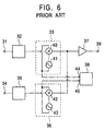
- Fig. 6 shows a conventional TV-signal receiving tuner.
- This V-U integrated-type TV-signal receiving tuner is formed by integrating a VHF-band TV-signal receiving tuner and a UHF-band TV-signal receiving tuner into one unit, and includes a VHF-band input terminal 31, a VHF-band high-frequency circuit section 32, a VHF-band frequency converter 33, a UHF-band input terminal 34, a UHF-band high-frequency circuit section 35, a UHF-band frequency converter 36, an intermediate-frequency amplifier 37, a band switcher 38, and an output terminal 39.
- the VHF-band frequency converter 33 has a VHF-band mixer 40 and a VHF-band local oscillator 41.
- the UHF-band frequency converter 36 has a UHF-band mixer 42 and a UHF-band local oscillator 43.
- the VHF-band high-frequency circuit section 32 includes a high-frequency amplifier, a tuning circuit, and a filter (none of them are shown), selects a VHF-band TV signal to be received, and amplifies it.
- the UHF-band high-frequency circuit section 35 includes a high-frequency amplifier, a tuning circuit, and a filter (none of them are shown), selects a UHF-band TV signal to be received, and amplifies it.
- the band switcher 38 is connected to the VHF-band frequency converter 33 and to the UHF-band frequency converter 36, and supplies a switching voltage to one of the VHF-band frequency converter 33 and the UHF-band frequency converter 36 according to the band to be received.
- the switching voltage is generated only at a first control terminal 44, the switching voltage is supplied to the VHF-band frequency converter 33, the VHF-band frequency converter 33 is set to an operating state, and the UHF-band frequency converter 36 is set to a not-operating state.
- the switching voltage is generated only at a second control terminal 45, the switching voltage is supplied to the UHF-band frequency converter 36, the UHF-band frequency converter 36 is set to an operating state, and the VHF-band frequency converter 33 is set to a not-operating state.
- the VHF-band TV signal received at an antenna passes through the VHF-band high-frequency circuit section 32, is frequency-converted by the VHF-band mixer 40 and the VHF-band local oscillator 41 in the VHF-band frequency converter 33, is amplified by the intermediate-frequency amplifier 37 as an intermediate-frequency signal IF, and is output from the output terminal 39.
- the intermediate-frequency signal IF output from the output terminal 39 is detected by a detection circuit (not shown).
- the UHF-band TV signal received at an antenna passes through the UHF-band high-frequency circuit section 35, is frequency-converted by the UHF-band mixer 42 and the UHF-band local oscillator 43 in the UHF-band frequency converter 36, is amplified by the intermediate-frequency amplifier 37 as an intermediate-frequency signal IF, and is output from the output terminal 39.
- the intermediate-frequency signal IF output from the output terminal 39 is detected by a detection circuit (not shown).
- an oscillation signal generated by the VHF-band local oscillator 41 leaks to the UHF-band frequency converter 36, and is emitted to the air through the UHF-band high-frequency circuit section 35 and the antenna.
- an oscillation signal generated by the UHF-band local oscillator 43 leaks to the VHF-band frequency converter 33, and is emitted to the air through the VHF-band high-frequency circuit section 32 and the antenna.
- a TV-signal receiving tuner for both VHF and UHF frequency bands, including a VHF-band frequency converter having a VHF-band mixer and a VHF-band local oscillator, for converting a VHF-band TV signal to a signal having an intermediate frequency; a UHF-band frequency converter having a UHF-band mixer and a UHF-band local oscillator, for converting a UHF-band TV signal to a signal having an intermediate frequency; and a band switcher for selectively operating the VHF-band frequency converter or the UHF-band frequency converter, wherein a switch circuit is provided for at least one of a previous stage of the VHF-band frequency converter and a previous stage of the UHF-band frequency converter; and the switch circuit passes a high-frequency signal when a frequency converter at a subsequent stage of the switch circuit is operating, and does not pass a high-frequency signal when the frequency converter at the subsequent stage of the switch circuit is not operating.
- the TV-signal receiving tuner may be formed such that a VHF-band high-frequency circuit section is provided at a previous stage of the VHF-band frequency converter; a UHF-band high-frequency circuit section is provided at a previous stage of the UHF-band frequency converter; and the switch circuit is provided at at least one of a location between the VHF-band high-frequency circuit section and the VHF-band frequency converter, and a location between the UHF-band high-frequency circuit section and the UHF-band frequency converter.
- the TV-signal receiving tuner may be formed such that the switch circuit is provided at at least one of a location immediately before the VHF-band frequency converter and a location immediately before the UHF-band frequency converter.
- the switch circuit can be combined with the frequency converter and other circuits into an integrated circuit to make the circuit compact.
- the TV-signal receiving tuner may be formed such that the switch circuit includes a transmission line to which an input end and an output end of the switch circuit are connected, and a transistor or a diode for making and breaking a connection between the transmission line and the ground is provided.
- the TV-signal receiving tuner may be formed such that the switch circuit is provided with a transistor or a diode for making and breaking a connection between an input end and an output end of the switch circuit.
- the switch circuit is formed of a transistor or a diode, the switch circuit is made compact and extraneous emission is suppressed without increasing the volume of the tuner.
- the TV-signal receiving tuner may be formed such that the switch circuit includes a transmission line to which an input end and an output end of the switch circuit are connected; a first transistor or a first diode for making and breaking a connection between the transmission line and the ground is provided; a second transistor or a second diode for making and breaking a connection between the input end and the output end is provided; and when the connection between the transmission line and the ground is broken, the connection between the input end and the output end is made, and when the connection between the transmission line and the ground is made, the connection between the input end and the output end is broken.
- this V-U integrated-type TV-signal receiving tuner is formed by integrating a VHF-band TV-signal receiving tuner and a UHF-band TV-signal receiving tuner into one unit, and includes a VHF-band input terminal 1, a VHF-band high-frequency circuit section 2, a first switch circuit 3, a VHF-band frequency converter 4, a UHF-band input terminal 5, a UHF-band high-frequency circuit section 6, a second switch circuit 7, a UHF-band frequency converter 8, an intermediate-frequency amplifier 9, a band switcher 10, and an output terminal 11.
- the VHF-band frequency converter 4 has a VHF-band mixer 12 and a VHF-band local oscillator 13.
- the UHF-band frequency converter 8 has a UHF-band mixer 14 and a UHF-band local oscillator 15.
- the VHF-band high-frequency circuit section 2 includes a high-frequency amplifier, a tuning circuit, and a filter (none of them are shown), selects a VHF-band TV signal to be received, and amplifies it.
- the UHF-band high-frequency circuit section 6 includes a high-frequency amplifier, a tuning circuit, and a filter (none of them are shown), selects a UHF-band TV signal to be received, and amplifies it.
- a part of the TV-signal receiving tuner is formed in an integrated circuit to be made compact.
- the first switch circuit 3, the VHF-band frequency converter 4, the second switch circuit 7, the UHF-band frequency converter 8, the intermediate-frequency amplifier 9, the band switcher 10, and others are formed in the integrated circuit as a unit. Since the VHF-band high-frequency circuit section 2 and the UHF-band high-frequency circuit section 6 have filters, it is difficult to form them in the integrated circuit. They are formed outside the integrated circuit.
- the band switcher 10 is connected to the first switch circuit 3, the VHF-band frequency converter 4, the second switch circuit 7, and the UHF-band frequency converter 8, and supplies a switching voltage according to the band to be received.
- the switching voltage is supplied only to a first control terminal 16, the switching voltage is supplied to the VHF-band frequency converter 4, and the VHF-band frequency converter 4 is set to an operating state.
- the switching voltage is sent to the first switch circuit 3, and the first switch circuit 3 is set such that the VHF-band TV signal output from the VHF-band high-frequency circuit section 2 passes through the first switch circuit 3 and is input to the VHF-band frequency converter 4.
- the switching voltage is not supplied to a second control terminal 17, and therefore, the UHF-band frequency converter 8 does not operate and the second switch circuit 7 is set such that a UHF-band TV signal leaking from the UHF-band high-frequency circuit section 6 cannot pass through the second switch circuit 7.
- the switching voltage is supplied only to the second control terminal 17, the switching voltage is supplied to the UHF-band frequency converter 8, and the UHF-band frequency converter 8 is set to an operating state.
- the switching voltage is sent to the second switch circuit 7, and the second switch circuit 7 is set such that the UHF-band TV signal output from the UHF-band high-frequency circuit section 6 passes through the second switch circuit 7 and is input to the UHF-band frequency converter 8.
- the switching voltage is not supplied to the first control terminal 16, and therefore, the VHF-band frequency converter 4 does not operate and the first switch circuit 3 is set such that a VHF-band TV signal leaking from the VHF-band high-frequency circuit section 2 cannot pass through the first switch circuit 3.
- the VHF-band TV signal received at an antenna passes through the VHF-band high-frequency circuit section 2 and then the first switch circuit 3, is frequency-converted by the VHF-band mixer 12 and the VHF-band local oscillator 13 in the VHF-band frequency converter 4, is amplified by the intermediate-frequency amplifier 9 as an intermediate-frequency signal IF, and is output from the output terminal 11.
- the intermediate-frequency signal IF output from the output terminal 11 is detected by a detection circuit (not shown).
- the second switch circuit 7 is set such that a signal cannot pass through the second switch circuit 7, even if an oscillation signal generated by the VHF-band local oscillator 13 leaks to the UHF-band frequency converter 8, the leakage is blocked by the second switch circuit 7. The leakage does not reach the antenna and extraneous emission is reduced.
- the UHF-band TV signal received at an antenna passes through the UHF-band high-frequency circuit section 6 and then the second switch circuit 7, is frequency-converted by the UHF-band mixer 14 and the UHF-band local oscillator 15 in the UHF-band frequency converter 8, is amplified by the intermediate-frequency amplifier 9 as an intermediate-frequency signal IF, and is output from the output terminal 11.
- the intermediate-frequency signal IF output from the output terminal 11 is detected by a detection circuit (not shown).
- the first switch circuit 3 is set such that a signal cannot pass through the first switch circuit 3, even if an oscillation signal generated by the UHF-band local oscillator 15 leaks to the VHF-band frequency converter 4, the leakage is blocked by the first switch circuit 3. The leakage does not reach the antenna and extraneous emission is reduced.
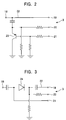
- a switch circuit shown in Fig. 2 includes a transistor which shunts a signal to the ground.
- a PNP transistor 23 is connected between the ground and a transmission line 22 connected to an input terminal 18 and an output terminal 19 of the switch circuit to shunt a signal on the transmission line to the ground.
- a power-source voltage is sent to the emitter of the transistor 23 through a power-source supply terminal 20, and the switching voltage is sent to the base through a switching-voltage input terminal 21.
- Fig. 3 shows a structure in which a diode is used to connect an input terminal 18 and an output terminal 19 or to disconnect them.
- a diode 24 is provided at the middle of a transmission line connected to the input terminal 18 and to the output terminal 19.
- a power-source voltage is sent to the cathode of the diode 24 from a power-source supply terminal 20, and the switching voltage is sent to the anode from a switching-voltage input terminal 21.
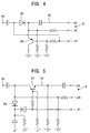
- Fig. 4 shows a structure in which a transistor for shunting a signal to the ground and a diode for connecting an input terminal and an output terminal and for disconnecting them are provided.
- a diode 25 is inserted at the middle of a transmission line 22 connecting an input terminal 18 and an output terminal 19, and a PNP transistor 26 is connected between the transmission line 22 and the ground.
- a power-source voltage is supplied from a power-source supply terminal 20 and the switching voltage is sent from a switching-voltage input terminal 21, to the diode 25 and to the transistor 26.
- Fig. 5 shows a structure in which a diode for shunting a signal to the ground and a transistor for connecting an input terminal and an output terminal and for disconnecting them are provided.
- An NPN transistor 27 is inserted at the middle of a transmission line 22 connecting an input terminal 18 and an output terminal 19, and a diode 28 is connected between the transmission line 22 and the ground.
- a power-source voltage is supplied from a power-source supply terminal 20 and the switching voltage is sent from a switching-voltage input terminal 21, to the transistor 27 and to the diode 28.
- All of the example switch circuits shown in Fig. 2 to Fig. 5 prevent an oscillation signal generated by the local oscillator from leaking from the antenna to the air. Since the switch circuits shown in Fig. 4 and Fig. 5 disconnect the transmission line 22 at the middle and ground it, they suppress extraneous emission to a lower level than that in the switch circuits shown in Fig. 2 and Fig. 3.
- a switch circuit may be provided at a previous stage of a high-frequency circuit section. Since the high-frequency circuit section has a filter, it is difficult to put the high-frequency circuit section into an integrated circuit. It is easier to make a circuit compact when a switch circuit is provided at a subsequent stage of the high-frequency circuit section and the switch circuit is integrated together with a frequency converter.
- a TV-signal receiving tuner of the present invention is not limited to those described above. Various modifications can be made within the scope of the present invention.
Landscapes
- Engineering & Computer Science (AREA)
- Multimedia (AREA)
- Signal Processing (AREA)
- Superheterodyne Receivers (AREA)
- Input Circuits Of Receivers And Coupling Of Receivers And Audio Equipment (AREA)
- Channel Selection Circuits, Automatic Tuning Circuits (AREA)
Abstract
Description
- The present invention relates to TV-signal receiving tuners, and more particularly, to a TV-signal receiving tuner for both VHF and UHF frequency bands, which prevents an oscillation signal of a local oscillator in the TV-signal receiving tuner from leaking.
- Fig. 6 shows a conventional TV-signal receiving tuner. This V-U integrated-type TV-signal receiving tuner is formed by integrating a VHF-band TV-signal receiving tuner and a UHF-band TV-signal receiving tuner into one unit, and includes a VHF-
band input terminal 31, a VHF-band high-frequency circuit section 32, a VHF-band frequency converter 33, a UHF-band input terminal 34, a UHF-band high-frequency circuit section 35, a UHF-band frequency converter 36, an intermediate-frequency amplifier 37, aband switcher 38, and anoutput terminal 39. The VHF-band frequency converter 33 has a VHF-band mixer 40 and a VHF-bandlocal oscillator 41. The UHF-band frequency converter 36 has a UHF-band mixer 42 and a UHF-bandlocal oscillator 43. - The VHF-band high-
frequency circuit section 32 includes a high-frequency amplifier, a tuning circuit, and a filter (none of them are shown), selects a VHF-band TV signal to be received, and amplifies it. - In the same way, the UHF-band high-
frequency circuit section 35 includes a high-frequency amplifier, a tuning circuit, and a filter (none of them are shown), selects a UHF-band TV signal to be received, and amplifies it. - The
band switcher 38 is connected to the VHF-band frequency converter 33 and to the UHF-band frequency converter 36, and supplies a switching voltage to one of the VHF-band frequency converter 33 and the UHF-band frequency converter 36 according to the band to be received. When a VHF-band TV signal is to be received, the switching voltage is generated only at afirst control terminal 44, the switching voltage is supplied to the VHF-band frequency converter 33, the VHF-band frequency converter 33 is set to an operating state, and the UHF-band frequency converter 36 is set to a not-operating state. When a UHF-band TV signal is to be received, the switching voltage is generated only at asecond control terminal 45, the switching voltage is supplied to the UHF-band frequency converter 36, the UHF-band frequency converter 36 is set to an operating state, and the VHF-band frequency converter 33 is set to a not-operating state. - When a VHF-band TV signal is received, the VHF-band TV signal received at an antenna (not shown) passes through the VHF-band high-
frequency circuit section 32, is frequency-converted by the VHF-band mixer 40 and the VHF-bandlocal oscillator 41 in the VHF-band frequency converter 33, is amplified by the intermediate-frequency amplifier 37 as an intermediate-frequency signal IF, and is output from theoutput terminal 39. The intermediate-frequency signal IF output from theoutput terminal 39 is detected by a detection circuit (not shown). - When a UHF-band TV signal is received, the UHF-band TV signal received at an antenna (not shown) passes through the UHF-band high-
frequency circuit section 35, is frequency-converted by the UHF-band mixer 42 and the UHF-bandlocal oscillator 43 in the UHF-band frequency converter 36, is amplified by the intermediate-frequency amplifier 37 as an intermediate-frequency signal IF, and is output from theoutput terminal 39. The intermediate-frequency signal IF output from theoutput terminal 39 is detected by a detection circuit (not shown). - In the above conventional V-U integrated-type TV-signal receiving tuner, since the distances between the circuits are short, isolation between the VHF-
band frequency converter 33 and the UHF-band frequency converter 36 cannot be sufficiently provided. Therefore, an oscillation signal generated by the local oscillator of an operating frequency converter leaks to the not-operating frequency converter, and is emitted from the antenna to the air to give disturbance to other receivers. - When a VHF-band TV signal is received, an oscillation signal generated by the VHF-band
local oscillator 41 leaks to the UHF-band frequency converter 36, and is emitted to the air through the UHF-band high-frequency circuit section 35 and the antenna. When a UHF-band TV signal is received, an oscillation signal generated by the UHF-bandlocal oscillator 43 leaks to the VHF-band frequency converter 33, and is emitted to the air through the VHF-band high-frequency circuit section 32 and the antenna. - Accordingly, it is an object of the present invention to provide a TV-signal receiving tuner which prevents a case in which an oscillation signal generated by an operating local oscillator leaks to an not-operating frequency converter and is emitted to the air through an antenna as extraneous emission to give disturbance to other receivers.
- The foregoing object is achieved by the present invention through the provision of a TV-signal receiving tuner for both VHF and UHF frequency bands, including a VHF-band frequency converter having a VHF-band mixer and a VHF-band local oscillator, for converting a VHF-band TV signal to a signal having an intermediate frequency; a UHF-band frequency converter having a UHF-band mixer and a UHF-band local oscillator, for converting a UHF-band TV signal to a signal having an intermediate frequency; and a band switcher for selectively operating the VHF-band frequency converter or the UHF-band frequency converter, wherein a switch circuit is provided for at least one of a previous stage of the VHF-band frequency converter and a previous stage of the UHF-band frequency converter; and the switch circuit passes a high-frequency signal when a frequency converter at a subsequent stage of the switch circuit is operating, and does not pass a high-frequency signal when the frequency converter at the subsequent stage of the switch circuit is not operating.
- Therefore, even if an oscillation signal generated by the local oscillator of the operating frequency converter leaks to the not-operating frequency converter, the oscillation signal is not emitted from the antenna to the air. Extraneous emission is suppressed.
- The TV-signal receiving tuner may be formed such that a VHF-band high-frequency circuit section is provided at a previous stage of the VHF-band frequency converter; a UHF-band high-frequency circuit section is provided at a previous stage of the UHF-band frequency converter; and the switch circuit is provided at at least one of a location between the VHF-band high-frequency circuit section and the VHF-band frequency converter, and a location between the UHF-band high-frequency circuit section and the UHF-band frequency converter.
- In this case, since the oscillation signal which causes extraneous emission can be blocked near the emission source, extraneous emission is effectively reduced.
- The TV-signal receiving tuner may be formed such that the switch circuit is provided at at least one of a location immediately before the VHF-band frequency converter and a location immediately before the UHF-band frequency converter.
- In this case, the switch circuit can be combined with the frequency converter and other circuits into an integrated circuit to make the circuit compact.
- The TV-signal receiving tuner may be formed such that the switch circuit includes a transmission line to which an input end and an output end of the switch circuit are connected, and a transistor or a diode for making and breaking a connection between the transmission line and the ground is provided.
- The TV-signal receiving tuner may be formed such that the switch circuit is provided with a transistor or a diode for making and breaking a connection between an input end and an output end of the switch circuit.
- In this case, since the switch circuit is formed of a transistor or a diode, the switch circuit is made compact and extraneous emission is suppressed without increasing the volume of the tuner.
- The TV-signal receiving tuner may be formed such that the switch circuit includes a transmission line to which an input end and an output end of the switch circuit are connected; a first transistor or a first diode for making and breaking a connection between the transmission line and the ground is provided; a second transistor or a second diode for making and breaking a connection between the input end and the output end is provided; and when the connection between the transmission line and the ground is broken, the connection between the input end and the output end is made, and when the connection between the transmission line and the ground is made, the connection between the input end and the output end is broken.
- In this case, since the transmission line of the switch circuit can be grounded and electrically disconnected at the same time, extraneous emission is further suppressed.
- Embodiments of the present invention will now be described, by way of example only, with reference to the accompanying drawings, in which:
- Fig. 1 is a block diagram of a TV-signal receiving tuner according to an embodiment of the present invention.
- Fig. 2 is a circuit diagram of a switch circuit used in the TV-signal receiving tuner according to the present embodiment.
- Fig. 3 is a circuit diagram of another switch circuit used in the TV-signal receiving tuner according to the present embodiment.
- Fig. 4 is a circuit diagram of yet another switch circuit used in the TV-signal receiving tuner according to the present embodiment.
- Fig. 5 is a circuit diagram of still another switch circuit used in the TV-signal receiving tuner according to the present embodiment.
- Fig. 6 is a block diagram of a conventional TV-signal receiving tuner.
-
- In Fig. 1, this V-U integrated-type TV-signal receiving tuner is formed by integrating a VHF-band TV-signal receiving tuner and a UHF-band TV-signal receiving tuner into one unit, and includes a VHF-band input terminal 1, a VHF-band high-
frequency circuit section 2, afirst switch circuit 3, a VHF-band frequency converter 4, a UHF-band input terminal 5, a UHF-band high-frequency circuit section 6, asecond switch circuit 7, a UHF-band frequency converter 8, an intermediate-frequency amplifier 9, aband switcher 10, and anoutput terminal 11. The VHF-band frequency converter 4 has a VHF-band mixer 12 and a VHF-bandlocal oscillator 13. The UHF-band frequency converter 8 has a UHF-band mixer 14 and a UHF-bandlocal oscillator 15. - The VHF-band high-
frequency circuit section 2 includes a high-frequency amplifier, a tuning circuit, and a filter (none of them are shown), selects a VHF-band TV signal to be received, and amplifies it. - In the same way, the UHF-band high-
frequency circuit section 6 includes a high-frequency amplifier, a tuning circuit, and a filter (none of them are shown), selects a UHF-band TV signal to be received, and amplifies it. - A part of the TV-signal receiving tuner is formed in an integrated circuit to be made compact. The
first switch circuit 3, the VHF-band frequency converter 4, thesecond switch circuit 7, the UHF-band frequency converter 8, the intermediate-frequency amplifier 9, theband switcher 10, and others are formed in the integrated circuit as a unit. Since the VHF-band high-frequency circuit section 2 and the UHF-band high-frequency circuit section 6 have filters, it is difficult to form them in the integrated circuit. They are formed outside the integrated circuit. - The
band switcher 10 is connected to thefirst switch circuit 3, the VHF-band frequency converter 4, thesecond switch circuit 7, and the UHF-band frequency converter 8, and supplies a switching voltage according to the band to be received. When a VHF-band TV signal is to be received, the switching voltage is supplied only to afirst control terminal 16, the switching voltage is supplied to the VHF-band frequency converter 4, and the VHF-band frequency converter 4 is set to an operating state. At the same time, the switching voltage is sent to thefirst switch circuit 3, and thefirst switch circuit 3 is set such that the VHF-band TV signal output from the VHF-band high-frequency circuit section 2 passes through thefirst switch circuit 3 and is input to the VHF-band frequency converter 4. In this case, the switching voltage is not supplied to asecond control terminal 17, and therefore, the UHF-band frequency converter 8 does not operate and thesecond switch circuit 7 is set such that a UHF-band TV signal leaking from the UHF-band high-frequency circuit section 6 cannot pass through thesecond switch circuit 7. - In the same way, when a UHF-band TV signal is to be received, the switching voltage is supplied only to the
second control terminal 17, the switching voltage is supplied to the UHF-band frequency converter 8, and the UHF-band frequency converter 8 is set to an operating state. At the same time, the switching voltage is sent to thesecond switch circuit 7, and thesecond switch circuit 7 is set such that the UHF-band TV signal output from the UHF-band high-frequency circuit section 6 passes through thesecond switch circuit 7 and is input to the UHF-band frequency converter 8. In this case, the switching voltage is not supplied to thefirst control terminal 16, and therefore, the VHF-band frequency converter 4 does not operate and thefirst switch circuit 3 is set such that a VHF-band TV signal leaking from the VHF-band high-frequency circuit section 2 cannot pass through thefirst switch circuit 3. - When a VHF-band TV signal is received, the VHF-band TV signal received at an antenna (not shown) passes through the VHF-band high-
frequency circuit section 2 and then thefirst switch circuit 3, is frequency-converted by the VHF-band mixer 12 and the VHF-bandlocal oscillator 13 in the VHF-band frequency converter 4, is amplified by the intermediate-frequency amplifier 9 as an intermediate-frequency signal IF, and is output from theoutput terminal 11. The intermediate-frequency signal IF output from theoutput terminal 11 is detected by a detection circuit (not shown). - In this case, since the
second switch circuit 7 is set such that a signal cannot pass through thesecond switch circuit 7, even if an oscillation signal generated by the VHF-bandlocal oscillator 13 leaks to the UHF-band frequency converter 8, the leakage is blocked by thesecond switch circuit 7. The leakage does not reach the antenna and extraneous emission is reduced. - When a UHF-band TV signal is received, the UHF-band TV signal received at an antenna (not shown) passes through the UHF-band high-
frequency circuit section 6 and then thesecond switch circuit 7, is frequency-converted by the UHF-band mixer 14 and the UHF-bandlocal oscillator 15 in the UHF-band frequency converter 8, is amplified by the intermediate-frequency amplifier 9 as an intermediate-frequency signal IF, and is output from theoutput terminal 11. The intermediate-frequency signal IF output from theoutput terminal 11 is detected by a detection circuit (not shown). - In this case, since the
first switch circuit 3 is set such that a signal cannot pass through thefirst switch circuit 3, even if an oscillation signal generated by the UHF-bandlocal oscillator 15 leaks to the VHF-band frequency converter 4, the leakage is blocked by thefirst switch circuit 3. The leakage does not reach the antenna and extraneous emission is reduced. - Specific examples of the
first switch circuit 3 will be described next by referring to Fig. 2 to Fig. 4. Since thesecond switch circuit 7 has the same structure as thefirst switch circuit 3, descriptions thereof will be omitted. A switch circuit shown in Fig. 2 includes a transistor which shunts a signal to the ground. APNP transistor 23 is connected between the ground and atransmission line 22 connected to aninput terminal 18 and anoutput terminal 19 of the switch circuit to shunt a signal on the transmission line to the ground. A power-source voltage is sent to the emitter of thetransistor 23 through a power-source supply terminal 20, and the switching voltage is sent to the base through a switching-voltage input terminal 21. - In the above structure, when a VHF-band TV signal is to be received, the switching voltage is sent to the base of the
transistor 23 from theband switcher 10 through the switching-voltage input terminal 21. Then, the emitter of thetransistor 23 is electrically disconnected from the collector. A VHF-band TV signal input to theinput terminal 18 passes through thetransmission line 22 and is output from theoutput terminal 19. - When a UHF-band TV signal is to be received, the switching voltage is not sent from the
band switcher 10 to the switching-voltage input terminal 21. Therefore, the emitter of thetransistor 23 is electrically connected to the collector, thetransmission line 22 is grounded, and a signal cannot pass through thetransmission line 22. Consequently, even if an oscillation signal generated by the UHF-bandlocal oscillator 15 is input to theoutput terminal 19 through the VHF-band frequency converter 4, the signal does not reach theinput terminal 18. The oscillation signal of the UHF-bandlocal oscillator 15 is prevented from leaking from the antenna to the air. - Fig. 3 shows a structure in which a diode is used to connect an
input terminal 18 and anoutput terminal 19 or to disconnect them. Adiode 24 is provided at the middle of a transmission line connected to theinput terminal 18 and to theoutput terminal 19. A power-source voltage is sent to the cathode of thediode 24 from a power-source supply terminal 20, and the switching voltage is sent to the anode from a switching-voltage input terminal 21. - In the above structure, when a VHF-band TV signal is to be received, the switching voltage is sent to the anode of the
diode 24 from theband switcher 10 through the switching-voltage input terminal 21. Then, thediode 24 becomes a continuity state. A VHF-band TV signal input to theinput terminal 18 passes through thetransmission line 22 and is output from theoutput terminal 19. - When a UHF-band TV signal is to be received, the switching voltage is not sent from the
band switcher 10 to the switching-voltage input terminal 21. Therefore, thediode 24 becomes a non-continuity state, and a signal cannot pass through thetransmission line 22. Consequently, even if an oscillation signal generated by the UHF-bandlocal oscillator 15 is input to theoutput terminal 19 through the VHF-band frequency converter 4, the signal does not reach theinput terminal 18. The oscillation signal of the UHF-bandlocal oscillator 15 is prevented from leaking from the antenna to the air. - Fig. 4 shows a structure in which a transistor for shunting a signal to the ground and a diode for connecting an input terminal and an output terminal and for disconnecting them are provided. A
diode 25 is inserted at the middle of atransmission line 22 connecting aninput terminal 18 and anoutput terminal 19, and aPNP transistor 26 is connected between thetransmission line 22 and the ground. A power-source voltage is supplied from a power-source supply terminal 20 and the switching voltage is sent from a switching-voltage input terminal 21, to thediode 25 and to thetransistor 26. - In the above structure, when a VHF-band TV signal is to be received, the switching voltage is sent to the anode of the
diode 25 and to the base of thetransistor 26 from theband switcher 10 through the switching-voltage input terminal 21. Then, thediode 25 becomes a continuity state and the emitter of thetransistor 26 is electrically not connected to the collector. As a result, a VHF-band TV signal input to theinput terminal 18 passes through thetransmission line 22 and is output from theoutput terminal 19. - When a UHF-band TV signal is to be received, the switching voltage is not sent from the
band switcher 10 to the switching-voltage input terminal 21. Therefore, thediode 25 becomes a non-continuity state, the emitter of thetransistor 26 is electrically connected to the collector, and the transmission line is grounded. Consequently, even if an oscillation signal generated by the UHF-bandlocal oscillator 15 is input to theoutput terminal 19 through the VHF-band frequency converter 4, the signal does not reach theinput terminal 18. The oscillation signal of the UHF-bandlocal oscillator 15 is prevented from leaking from the antenna to the air. - Fig. 5 shows a structure in which a diode for shunting a signal to the ground and a transistor for connecting an input terminal and an output terminal and for disconnecting them are provided. An
NPN transistor 27 is inserted at the middle of atransmission line 22 connecting aninput terminal 18 and anoutput terminal 19, and adiode 28 is connected between thetransmission line 22 and the ground. A power-source voltage is supplied from a power-source supply terminal 20 and the switching voltage is sent from a switching-voltage input terminal 21, to thetransistor 27 and to thediode 28. - In the above structure, when a VHF-band TV signal is to be received, the switching voltage is sent to the base of the
transistor 27 and to the cathode of thediode 28 from theband switcher 10 through the switching-voltage input terminal 21. Then, thetransistor 27 becomes a continuity state and thediode 28 becomes a non-continuity state. As a result, a TV signal input to theinput terminal 18 passes through thetransmission line 22 and is output from theoutput terminal 19. - When a UHF-band TV signal is to be received, the switching voltage is not sent from the
band switcher 10 to the switching-voltage input terminal 21. Therefore, thetransistor 27 becomes a non-continuity state, thediode 28 becomes a continuity state, and the transmission line is grounded. Consequently, even if an oscillation signal generated by the UHF-bandlocal oscillator 15 is input to theoutput terminal 19 through the VHF-band frequency converter 4, the signal does not reach theinput terminal 18. The oscillation signal of the UHF-bandlocal oscillator 15 is prevented from leaking from the antenna to the air. - All of the example switch circuits shown in Fig. 2 to Fig. 5 prevent an oscillation signal generated by the local oscillator from leaking from the antenna to the air. Since the switch circuits shown in Fig. 4 and Fig. 5 disconnect the
transmission line 22 at the middle and ground it, they suppress extraneous emission to a lower level than that in the switch circuits shown in Fig. 2 and Fig. 3. - A switch circuit may be provided at a previous stage of a high-frequency circuit section. Since the high-frequency circuit section has a filter, it is difficult to put the high-frequency circuit section into an integrated circuit. It is easier to make a circuit compact when a switch circuit is provided at a subsequent stage of the high-frequency circuit section and the switch circuit is integrated together with a frequency converter.
- A TV-signal receiving tuner of the present invention is not limited to those described above. Various modifications can be made within the scope of the present invention.
Claims (6)
- A TV-signal receiving tuner for both VHF and UHF frequency bands, comprising:a VHF-band frequency converter having a VHF-band mixer and a VHF-band local oscillator, for converting a VHF-band TV signal to a signal having an intermediate frequency;a UHF-band frequency converter having a UHF-band mixer and a UHF-band local oscillator, for converting a UHF-band TV signal to a signal having an intermediate frequency; anda band switcher for selectively operating said VHF-band frequency converter or said UHF-band frequency converter,
wherein a switch circuit is provided for at least one of a previous stage of said VHF-band frequency converter and a previous stage of said UHF-band frequency converter; andthe switch circuit passes a high-frequency signal when a frequency converter at a subsequent stage of the switch circuit is operating, and does not pass a high-frequency signal when the frequency converter at the subsequent stage of the switch circuit is not operating. - A TV-signal receiving tuner according to Claim 1, wherein a VHF-band high-frequency circuit section is provided at a previous stage of said VHF-band frequency converter; a UHF-band high-frequency circuit section is provided at a previous stage of said UHF-band frequency converter; and the switch circuit is provided at at least one of a location between the VHF-band high-frequency circuit section and said VHF-band frequency converter, and a location between the UHF-band high-frequency circuit section and said UHF-band frequency converter.
- A TV-signal receiving tuner according to Claim 1or 2 wherein the switch circuit is provided at at least one of a location immediately before said VHF-band frequency converter and a location immediately before said UHF-band frequency converter.
- A TV-signal receiving tuner according to Claim 1,2or 3 wherein the switch circuit includes a transmission line to which an input end and an output end of the switch circuit are connected, and a transistor or a diode for making and breaking a connection between the transmission line and the ground is provided.
- A TV-signal receiving tuner according to any preceding Claim wherein the switch circuit is provided with a transistor or a diode for making and breaking a connection between an input end and an output end of the switch circuit.
- A TV-signal receiving tuner according to any preceding Claim
wherein the switch circuit includes a transmission line to which an input end and an output end of the switch circuit are connected;a first transistor or a first diode for making and breaking a connection between the transmission line and the ground is provided;a second transistor or a second diode for making and breaking a connection between the input end and the output end is provided; andwhen the connection between the transmission line and the ground is broken, the connection between the input end and the output end is made, and when the connection between the transmission line and the ground is made, the connection between the input end and the output end is broken.
Applications Claiming Priority (2)
| Application Number | Priority Date | Filing Date | Title |
|---|---|---|---|
| JP02737399A JP3986195B2 (en) | 1999-02-04 | 1999-02-04 | TV signal receiving tuner |
| JP2737399 | 1999-02-04 |
Publications (2)
| Publication Number | Publication Date |
|---|---|
| EP1026885A1 true EP1026885A1 (en) | 2000-08-09 |
| EP1026885B1 EP1026885B1 (en) | 2005-07-13 |
Family
ID=12219253
Family Applications (1)
| Application Number | Title | Priority Date | Filing Date |
|---|---|---|---|
| EP00300241A Expired - Lifetime EP1026885B1 (en) | 1999-02-04 | 2000-01-14 | TV-signal receiving tuner with reduced extraneous emission |
Country Status (8)
| Country | Link |
|---|---|
| US (1) | US6639630B2 (en) |
| EP (1) | EP1026885B1 (en) |
| JP (1) | JP3986195B2 (en) |
| KR (1) | KR100366820B1 (en) |
| CN (1) | CN1128541C (en) |
| DE (1) | DE60021215T2 (en) |
| MX (1) | MXPA00001229A (en) |
| MY (1) | MY122286A (en) |
Cited By (3)
| Publication number | Priority date | Publication date | Assignee | Title |
|---|---|---|---|---|
| US8553526B2 (en) | 2006-09-28 | 2013-10-08 | Qualcomm Incorporated | Methods and apparatus for determining quality of service in a communication system |
| US9136955B2 (en) | 2009-06-30 | 2015-09-15 | Thomson Licensing | Method of resending digital signals |
| US9191226B2 (en) | 2006-09-28 | 2015-11-17 | Qualcomm Incorporated | Methods and apparatus for determining communication link quality |
Families Citing this family (10)
| Publication number | Priority date | Publication date | Assignee | Title |
|---|---|---|---|---|
| GB2367700A (en) * | 2000-10-06 | 2002-04-10 | Mitel Semiconductor Ltd | A single conversion tuner comprising a tracking filter and an image reject mixer |
| EP1265360B2 (en) | 2001-06-08 | 2012-08-15 | Alps Electric Co., Ltd. | Integrated television tuner with a band switching circuit |
| US6950152B2 (en) * | 2001-10-18 | 2005-09-27 | Alps Electric Co., Ltd. | Television tuner which has leveled a gain deviation in the same band |
| JP3099083U (en) * | 2003-07-07 | 2004-03-25 | アルプス電気株式会社 | Television tuner |
| JP3106226U (en) | 2004-06-28 | 2004-12-16 | アルプス電気株式会社 | Television tuner |
| DE102008018356A1 (en) * | 2008-04-11 | 2009-10-15 | Diehl Ako Stiftung & Co. Kg | clothes dryer |
| JP5763485B2 (en) * | 2011-09-16 | 2015-08-12 | ルネサスエレクトロニクス株式会社 | Antenna switch and communication device |
| CN105207692B (en) * | 2015-08-31 | 2018-08-03 | 海能达通信股份有限公司 | The method that time slot power is closed in wireless telecommunications system and its control |
| CN106130593B (en) * | 2016-06-29 | 2018-11-23 | 华讯方舟科技(湖北)有限公司 | Double-receiving microwave frequency conversion circuit and microwave frequency converter |
| CN107425923B (en) * | 2017-09-04 | 2024-05-14 | 林宇 | Magnetic fiber receiver and too wide magnetic fiber receiver |
Citations (6)
| Publication number | Priority date | Publication date | Assignee | Title |
|---|---|---|---|---|
| FR2367394A1 (en) * | 1976-10-11 | 1978-05-05 | Pizon Bros | Multi-standard television receiver circuit - automatically switches to UHF or VHF operation changing both IF and output stages |
| FR2454237A1 (en) * | 1979-04-12 | 1980-11-07 | Blaupunkt Werke Gmbh | TV tuner and IF stage screening housing - has UHF and VHF tuners mixers and IF stages completely screened and internally individually further screened |
| JPS60136408A (en) * | 1983-12-26 | 1985-07-19 | Matsushita Electric Ind Co Ltd | High frequency signal switching device |
| EP0348697A2 (en) * | 1988-06-28 | 1990-01-03 | TELEFUNKEN electronic GmbH | Television tuner |
| JPH06121249A (en) * | 1992-10-08 | 1994-04-28 | Matsushita Electric Ind Co Ltd | Automatic gain control device |
| EP0851580A1 (en) * | 1996-12-26 | 1998-07-01 | SHARP Corporation | Tuner for cable modem |
Family Cites Families (9)
| Publication number | Priority date | Publication date | Assignee | Title |
|---|---|---|---|---|
| US4499495A (en) * | 1982-07-26 | 1985-02-12 | Zenith Electronics Corporation | Switching diplexer for single antenna input television receivers |
| JPH01168125A (en) * | 1987-12-23 | 1989-07-03 | Matsushita Electric Ind Co Ltd | television tuner |
| US5115317A (en) * | 1989-12-22 | 1992-05-19 | Alps Electric Co., Ltd. | Tuning apparatus for a television receiver including selectively activated amplifier and local oscillator circuits |
| JP3092540B2 (en) | 1997-02-20 | 2000-09-25 | 日本電気株式会社 | High frequency receiving circuit |
| JPH10271401A (en) | 1997-03-25 | 1998-10-09 | Alps Electric Co Ltd | Television tuner and television receiver provided with the same |
| JP3597344B2 (en) * | 1997-07-30 | 2004-12-08 | アルプス電気株式会社 | Television signal receiving tuner and television signal receiving unit for personal computer |
| JPH11127086A (en) * | 1997-08-19 | 1999-05-11 | Alps Electric Co Ltd | UHF and VHF shared tuner |
| JP3183332B2 (en) * | 1997-09-30 | 2001-07-09 | 日本電気株式会社 | TV tuner, tuner IC, and TV tuner control method |
| KR20010012564A (en) * | 1998-03-13 | 2001-02-15 | 요트.게.아. 롤페즈 | Tuning with diode detector |
-
1999
- 1999-02-04 JP JP02737399A patent/JP3986195B2/en not_active Expired - Fee Related
-
2000
- 2000-01-14 DE DE60021215T patent/DE60021215T2/en not_active Expired - Lifetime
- 2000-01-14 EP EP00300241A patent/EP1026885B1/en not_active Expired - Lifetime
- 2000-01-28 MY MYPI20000314A patent/MY122286A/en unknown
- 2000-02-01 US US09/494,960 patent/US6639630B2/en not_active Expired - Fee Related
- 2000-02-01 CN CN00100481A patent/CN1128541C/en not_active Expired - Fee Related
- 2000-02-03 KR KR10-2000-0005364A patent/KR100366820B1/en not_active Expired - Fee Related
- 2000-02-03 MX MXPA00001229A patent/MXPA00001229A/en not_active IP Right Cessation
Patent Citations (6)
| Publication number | Priority date | Publication date | Assignee | Title |
|---|---|---|---|---|
| FR2367394A1 (en) * | 1976-10-11 | 1978-05-05 | Pizon Bros | Multi-standard television receiver circuit - automatically switches to UHF or VHF operation changing both IF and output stages |
| FR2454237A1 (en) * | 1979-04-12 | 1980-11-07 | Blaupunkt Werke Gmbh | TV tuner and IF stage screening housing - has UHF and VHF tuners mixers and IF stages completely screened and internally individually further screened |
| JPS60136408A (en) * | 1983-12-26 | 1985-07-19 | Matsushita Electric Ind Co Ltd | High frequency signal switching device |
| EP0348697A2 (en) * | 1988-06-28 | 1990-01-03 | TELEFUNKEN electronic GmbH | Television tuner |
| JPH06121249A (en) * | 1992-10-08 | 1994-04-28 | Matsushita Electric Ind Co Ltd | Automatic gain control device |
| EP0851580A1 (en) * | 1996-12-26 | 1998-07-01 | SHARP Corporation | Tuner for cable modem |
Non-Patent Citations (2)
| Title |
|---|
| PATENT ABSTRACTS OF JAPAN vol. 009, no. 298 (E - 361) 26 November 1985 (1985-11-26) * |
| PATENT ABSTRACTS OF JAPAN vol. 018, no. 407 (E - 1586) 29 July 1994 (1994-07-29) * |
Cited By (3)
| Publication number | Priority date | Publication date | Assignee | Title |
|---|---|---|---|---|
| US8553526B2 (en) | 2006-09-28 | 2013-10-08 | Qualcomm Incorporated | Methods and apparatus for determining quality of service in a communication system |
| US9191226B2 (en) | 2006-09-28 | 2015-11-17 | Qualcomm Incorporated | Methods and apparatus for determining communication link quality |
| US9136955B2 (en) | 2009-06-30 | 2015-09-15 | Thomson Licensing | Method of resending digital signals |
Also Published As
| Publication number | Publication date |
|---|---|
| KR20000057908A (en) | 2000-09-25 |
| DE60021215T2 (en) | 2006-01-05 |
| KR100366820B1 (en) | 2003-01-08 |
| CN1263416A (en) | 2000-08-16 |
| JP2000224007A (en) | 2000-08-11 |
| US6639630B2 (en) | 2003-10-28 |
| CN1128541C (en) | 2003-11-19 |
| US20030174254A1 (en) | 2003-09-18 |
| DE60021215D1 (en) | 2005-08-18 |
| EP1026885B1 (en) | 2005-07-13 |
| JP3986195B2 (en) | 2007-10-03 |
| MXPA00001229A (en) | 2002-03-08 |
| MY122286A (en) | 2006-04-29 |
Similar Documents
| Publication | Publication Date | Title |
|---|---|---|
| US6639630B2 (en) | TV-signal receiving tuner with reduced extraneous emission | |
| US4592093A (en) | Super high frequency receiver | |
| US6600897B1 (en) | Satellite-broadcasting receiving converter with a plurality of output terminals | |
| EP0346495B1 (en) | Television tuner | |
| US6307599B1 (en) | Analog-digital broadcast shared receiving tuner | |
| JP3547292B2 (en) | Television signal receiving tuner | |
| JP3490023B2 (en) | TV signal receiving tuner | |
| US6344881B1 (en) | Television tuner capable of receiving CATV broadcasting signal and ground wave FM broadcasting signal | |
| EP1137179A2 (en) | Television tuner | |
| US6791626B2 (en) | Input switching circuit for a television tuner immune to interference due to FM broadcasting signal | |
| JP3929818B2 (en) | Intermediate frequency circuit of television tuner | |
| US20040031064A1 (en) | Cable receiver having in-band and out-of-band tuners | |
| US7224408B2 (en) | Television tuner in which the number of integrated circuits can be reduced | |
| US3458819A (en) | Uhf-if or vhf-if converter | |
| JPH0117876Y2 (en) | ||
| JP3558848B2 (en) | Television tuner input circuit | |
| US20020052184A1 (en) | Avoidance of interference between items of electrical apparatus | |
| US20050122436A1 (en) | Television tuner which does not deteriorate picture quality even at the time of weak electric field | |
| US7366487B2 (en) | Receiving band switching circuit with reduced signal loss upon switching receiving band | |
| KR19980017760A (en) | RF Amplifier Common Unit for Television Tuner | |
| JPH1155582A (en) | Telephone signal reception unit | |
| JPH0746497A (en) | Receiver | |
| EP1263138A1 (en) | Television tuner | |
| JP2005348234A (en) | Television tuner | |
| JPH10242830A (en) | High-frequency signal connecting device |
Legal Events
| Date | Code | Title | Description |
|---|---|---|---|
| PUAI | Public reference made under article 153(3) epc to a published international application that has entered the european phase |
Free format text: ORIGINAL CODE: 0009012 |
|
| 17P | Request for examination filed |
Effective date: 20000429 |
|
| AK | Designated contracting states |
Kind code of ref document: A1 Designated state(s): DE FR GB |
|
| AX | Request for extension of the european patent |
Free format text: AL;LT;LV;MK;RO;SI |
|
| AKX | Designation fees paid |
Free format text: DE FR GB |
|
| 17Q | First examination report despatched |
Effective date: 20040315 |
|
| GRAP | Despatch of communication of intention to grant a patent |
Free format text: ORIGINAL CODE: EPIDOSNIGR1 |
|
| GRAS | Grant fee paid |
Free format text: ORIGINAL CODE: EPIDOSNIGR3 |
|
| GRAA | (expected) grant |
Free format text: ORIGINAL CODE: 0009210 |
|
| AK | Designated contracting states |
Kind code of ref document: B1 Designated state(s): DE FR GB |
|
| REG | Reference to a national code |
Ref country code: GB Ref legal event code: FG4D |
|
| RIN1 | Information on inventor provided before grant (corrected) |
Inventor name: OSADA, SHIGERU Inventor name: SATO, YOSHIHIRO Inventor name: YAMAMOTO, MASAKI |
|
| REF | Corresponds to: |
Ref document number: 60021215 Country of ref document: DE Date of ref document: 20050818 Kind code of ref document: P |
|
| ET | Fr: translation filed | ||
| PLBE | No opposition filed within time limit |
Free format text: ORIGINAL CODE: 0009261 |
|
| STAA | Information on the status of an ep patent application or granted ep patent |
Free format text: STATUS: NO OPPOSITION FILED WITHIN TIME LIMIT |
|
| 26N | No opposition filed |
Effective date: 20060418 |
|
| PGFP | Annual fee paid to national office [announced via postgrant information from national office to epo] |
Ref country code: GB Payment date: 20101215 Year of fee payment: 12 |
|
| PGFP | Annual fee paid to national office [announced via postgrant information from national office to epo] |
Ref country code: FR Payment date: 20120111 Year of fee payment: 13 |
|
| GBPC | Gb: european patent ceased through non-payment of renewal fee |
Effective date: 20130114 |
|
| REG | Reference to a national code |
Ref country code: FR Ref legal event code: ST Effective date: 20130930 |
|
| PG25 | Lapsed in a contracting state [announced via postgrant information from national office to epo] |
Ref country code: FR Free format text: LAPSE BECAUSE OF NON-PAYMENT OF DUE FEES Effective date: 20130131 Ref country code: GB Free format text: LAPSE BECAUSE OF NON-PAYMENT OF DUE FEES Effective date: 20130114 |
|
| PGFP | Annual fee paid to national office [announced via postgrant information from national office to epo] |
Ref country code: DE Payment date: 20140131 Year of fee payment: 15 |
|
| REG | Reference to a national code |
Ref country code: DE Ref legal event code: R119 Ref document number: 60021215 Country of ref document: DE |
|
| PG25 | Lapsed in a contracting state [announced via postgrant information from national office to epo] |
Ref country code: DE Free format text: LAPSE BECAUSE OF NON-PAYMENT OF DUE FEES Effective date: 20150801 |