EP1026742A2 - Solder ball grid array for connecting multiple millimeter wave assemblies - Google Patents
Solder ball grid array for connecting multiple millimeter wave assemblies Download PDFInfo
- Publication number
- EP1026742A2 EP1026742A2 EP00101673A EP00101673A EP1026742A2 EP 1026742 A2 EP1026742 A2 EP 1026742A2 EP 00101673 A EP00101673 A EP 00101673A EP 00101673 A EP00101673 A EP 00101673A EP 1026742 A2 EP1026742 A2 EP 1026742A2
- Authority
- EP
- European Patent Office
- Prior art keywords
- coaxial
- grid array
- ball grid
- disposed
- electrically conductive
- Prior art date
- Legal status (The legal status is an assumption and is not a legal conclusion. Google has not performed a legal analysis and makes no representation as to the accuracy of the status listed.)
- Withdrawn
Links
Images

Classifications
-
- H—ELECTRICITY
- H10—SEMICONDUCTOR DEVICES; ELECTRIC SOLID-STATE DEVICES NOT OTHERWISE PROVIDED FOR
- H10W—GENERIC PACKAGES, INTERCONNECTIONS, CONNECTORS OR OTHER CONSTRUCTIONAL DETAILS OF DEVICES COVERED BY CLASS H10
- H10W44/00—Electrical arrangements for controlling or matching impedance
- H10W44/20—Electrical arrangements for controlling or matching impedance at high-frequency [HF] or radio frequency [RF]
-
- H—ELECTRICITY
- H01—ELECTRIC ELEMENTS
- H01P—WAVEGUIDES; RESONATORS, LINES, OR OTHER DEVICES OF THE WAVEGUIDE TYPE
- H01P1/00—Auxiliary devices
- H01P1/04—Fixed joints
- H01P1/045—Coaxial joints
-
- H—ELECTRICITY
- H05—ELECTRIC TECHNIQUES NOT OTHERWISE PROVIDED FOR
- H05K—PRINTED CIRCUITS; CASINGS OR CONSTRUCTIONAL DETAILS OF ELECTRIC APPARATUS; MANUFACTURE OF ASSEMBLAGES OF ELECTRICAL COMPONENTS
- H05K1/00—Printed circuits
- H05K1/02—Details
- H05K1/0213—Electrical arrangements not otherwise provided for
- H05K1/0237—High frequency adaptations
- H05K1/0243—Printed circuits associated with mounted high frequency components
-
- H—ELECTRICITY
- H05—ELECTRIC TECHNIQUES NOT OTHERWISE PROVIDED FOR
- H05K—PRINTED CIRCUITS; CASINGS OR CONSTRUCTIONAL DETAILS OF ELECTRIC APPARATUS; MANUFACTURE OF ASSEMBLAGES OF ELECTRICAL COMPONENTS
- H05K2201/00—Indexing scheme relating to printed circuits covered by H05K1/00
- H05K2201/09—Shape and layout
- H05K2201/09209—Shape and layout details of conductors
- H05K2201/09654—Shape and layout details of conductors covering at least two types of conductors provided for in H05K2201/09218 - H05K2201/095
- H05K2201/09809—Coaxial layout
-
- H—ELECTRICITY
- H05—ELECTRIC TECHNIQUES NOT OTHERWISE PROVIDED FOR
- H05K—PRINTED CIRCUITS; CASINGS OR CONSTRUCTIONAL DETAILS OF ELECTRIC APPARATUS; MANUFACTURE OF ASSEMBLAGES OF ELECTRICAL COMPONENTS
- H05K2201/00—Indexing scheme relating to printed circuits covered by H05K1/00
- H05K2201/10—Details of components or other objects attached to or integrated in a printed circuit board
- H05K2201/10613—Details of electrical connections of non-printed components, e.g. special leads
- H05K2201/10621—Components characterised by their electrical contacts
- H05K2201/10734—Ball grid array [BGA]; Bump grid array
-
- H—ELECTRICITY
- H10—SEMICONDUCTOR DEVICES; ELECTRIC SOLID-STATE DEVICES NOT OTHERWISE PROVIDED FOR
- H10W—GENERIC PACKAGES, INTERCONNECTIONS, CONNECTORS OR OTHER CONSTRUCTIONAL DETAILS OF DEVICES COVERED BY CLASS H10
- H10W44/00—Electrical arrangements for controlling or matching impedance
- H10W44/20—Electrical arrangements for controlling or matching impedance at high-frequency [HF] or radio frequency [RF]
- H10W44/203—Electrical connections
- H10W44/209—Vertical interconnections, e.g. vias
- H10W44/212—Coaxial feed-throughs in substrates
Definitions
- the present invention relates generally to interconnection devices and more particularly to interconnection devices for mounting high-frequency multiple millimeter wave assemblies to circuit boards.
- BGA packages tend to be particularly popular because they are easier to surface mount on a printed circuit board than fine pitch peripheral lead packages, such as QFPs. This is because the outer leads of BGA packages are distributed on the lower surface of the package, rather than being restricted to the package perimeter and thus being easier to damage. Moreover, since BGA packages do not include peripheral leads, BGA packages take up less room on a printed circuit board, and may be closely spaced. This close spacing also allows for shorter interconnect lengths between packages, which results in improved electrical performance.
- IMAs high frequency integrated microwave assemblies
- BGA packages fail to address the specific needs of high frequency integrated microwave assemblies (IMAs), particularly with respect to providing low loss, reproducible electrical interconnections at the circuit board level for mounting high frequency IMAs.
- known packaging techniques fail to provide the interconnections which would allow high frequency signal generation, signal reception and digital processing to be combined in a compact space, such as a single circuit board. Rather, separate high frequency coaxial connectors are required to interface the high frequency IMAs with the circuit board.
- Coaxial transmission lines commonly employed for the propagation of microwave power in IMAs, include a cylindrical center conductor disposed within a cylindrical tubular outer conductor. Although more costly than open-wire transmission lines, coaxial lines completely enclose the electromagnetic fields, preventing radiation losses and providing shielding from nearby circuits. With a coaxial connector, signal loss is minimized since almost all of the electric field emanating from the signal conductor remains confined in the dielectric. A coaxial conductor will thus electrically insulate the central signal path from any other signals in the vicinity.
- Deficiencies can exist with respect to performance in IMAs, particularly at very high frequencies if such interconnections are not properly accommodated. This is because slight variations in signal path impedance may dramatically impact transmission performance. Furthermore, the high frequency interconnection needs to be inexpensive, allowing its use in the commercial market place.
- the present invention provides an apparatus for interfacing with a coaxial device having a central and ground conductor, including a plurality of electrically conductive structures disposed in an array, including a centrally disposed structure for receiving the central conductor and a plurality of ground structures disposed about the centrally disposed structure for receiving the ground conductor.
- the present invention provides a high frequency coaxial interconnection ball grid array for providing connection to a coaxial line having a first and second conductor, including a center disposed electrically conductive ball for interfacing with the first conductor and a plurality of outer electrically conductive balls disposed about the center disposed ball for interfacing with the second conductor.
- the present invention provides a packaging structure, including a circuit board, a circuit board chip package connected to the circuit board wherein the circuit board chip package includes at least one coaxial interface having a central and ground conductor and a plurality of electrically conductive structures disposed in an array, including a centrally disposed structure for receiving the central conductor and a plurality of ground structures disposed about the centrally disposed structure for receiving the ground conductor, wherein the array is disposed between the circuit board and the circuit board chip package.
- the present invention provides a high frequency interconnection ball grid array for coaxially interconnecting an integrated microwave assembly with a circuit board assembly, including a center disposed solder ball for mating with an inner conductor of a coaxial line and a plurality of outer disposed solder balls for mating with an outer conductor of the coaxial line.
- a high frequency coaxial interconnection ball grid array 10 for producing a low loss, reproducible electrical interconnection at the circuit board level for mounting one or more high frequency components 12, such as high frequency IMA modules, is illustrated.
- arrays of coaxial lines, extending from the high frequency component to be mounted may be connected to a circuit board at millimeter wave frequencies (typically up to 60 Ghz).
- millimeter wave frequencies typically up to 60 Ghz.
- the coaxial interconnection ball grid array 10 is preferably implemented with solder connections, although other connections, including but not limited to, epoxy coiled wire (Fuzz butter) and gold connections may be used as well.
- the high frequency coaxial interconnection ball grid array 10 of the present invention is not limited to the specific configurations shown and discussed herein. Any interconnect structure that uses a predetermined geometrical pattern of conductive balls, bumps, or other objects to provide a high-isolation-interconnect structure between a printed wiring board and an active microwave component may be utilized. Further, the present invention is not limited to providing interconnection for high frequency IMA modules, but rather may be utilized to interconnect integrated circuit (IC) assembly modules or circuit board chip package in general. Such integrated circuit assembly modules may include, but are not limited to, full- and semi-custom application specific integrated circuits (ASICs) and other high performance IC chips. Nor is the present invention limited to connecting IC assembly modules to printed circuit boards.
- ASICs application specific integrated circuits
- coaxial interconnection ball grid array 10 of the present invention may be utilized to connect the modules to any electronic component having a coaxial interface. It is thus understood that there are many other configurations which may utilize the coaxial-like high frequency interconnection of the present invention which are shown and discussed herein.
- the coaxial interconnection ball grid array 10 interconnects the coaxial port of a millimeter wave module 12 with a coaxial port on an electronic component, such as a polymeric circuit board 14.
- the present invention connects high frequency signals up to 60 Ghz from a circuit board 14 to a millimeter wave module 12, thereby allowing highly integrated microwave networks to be built from a plurality of modules 12.
- the millimeter wave modules 12 which may be interconnected utilizing the present invention include, but are not limited to, high frequency transmitters, receivers or oscillators.
- a coaxial-like interconnection is formed from a plurality of solder balls configured preferably in a three-by-three square array 10.
- the coaxial interconnection ball grid array 10 includes a single centrally disposed solder ball 16 for interconnecting with a centrally disposed conductor 18 of a coaxial line 26.
- the coaxial interconnection ball grid array 10 also includes a plurality of solder balls 20 and 22 surrounding the single centrally disposed solder ball 16, some balls 20 of which interconnect with a coaxial ground shield 24 of the coaxial line 26.
- Each center conductor 18 of a connecting coaxial line 26 is thus interconnected utilizing a single solder ball 16.
- the centrally disposed solder ball 16 and centrally disposed conductor 18 have the appearance of a rod with a diameter having a standard 50 ohm impedance.
- the outer conductive shield 24 or ground signal path of the coaxial line 26 is connected with multiple solder balls 20, to achieve a lower inductance ground-to-ground connection.
- the solder balls 20 are soldered to the shield 24 on the circuit board 14.
- the center conductor 18 of the coaxial line 26 is connected to the center solder ball 16 and the outer conductor 24 of the same coaxial line 26 is connected to the four solder balls 20 located closest to the center solder ball 16.
- each of the solder balls 16, 20 and 22 is preferably substantially the same, with the diameter determined by the center conductoris frequency and impedance requirement, thereby minimizing manufacturing costs.
- the diameter of and the spacing between each ball should be such that the coaxial interconnection ball grid array 10 electrically matches the impedance of the coaxial line 26, which for an example implementations in glass/epoxy for frequencies in the range of about 0 to 47.8 Ghz, typically has a dielectric constant of about 4.2, characteristic impedance of about 50 ohms, center conductor inside diameter of about 11.7 mils (0.00461 cm) and outer conductor inside diameter of about 65 mils (0.02559 cm).
- the diameter of each solder ball 16, 20 and 22 is preferably about 13 mils (0.00512 cm), with a tolerance of about +/- 2 mils (0.00079 cm). At a diameter of 13 mils, the discontinuity in a typical transmission line is minimized.
- the solder balls 16, 20 and 22 are preferably substantially equally spaced and positioned along the same plane. Assuming a ball diameter of 13 mils (0.00512 cm), the solder balls 16, 20 and 22 are preferably spaced about 30 mils (0.0118 cm) center-to-center from each other, with a tolerance of about +/- 2 mils (0.00079 cm).
- the cutoff frequency of the next higher order mode is about 47.8 Ghz.
- the present invention is not, however, limited to operation at about 47.8 Ghz and below with the particular dimensions noted above. Rather, the present invention can be utilized at frequencies higher than 47.8 Ghz, such as from about 0 to 60 Ghz, by feeding the coaxial interconnection ball grid array 10 straight as illustrated in FIG. 1 such that the next higher order mode is not excited.
- the diameter of and distance between adjacent solder balls 16, 20 and 22 may be adjusted to accommodate the connecting coax and provide the desired frequency and impedance requirement.
- board materials may be changed to provide suitable dielective constraints. In order to raise the higher mode cutoff frequency, the ball diameter and grid array size would generally have to be reduced.
- solder balls 16, 20 and 22 may be commercially available solder balls, such as those constructed of 90% Pb to 10% Sn or 63% Pb to 37% Sn, and during manufacture may be initially heated and cooled to form a solder connection between the IMA modules 12 and the circuit board 14.
- the method of manufacture of the solder ball array 10 is not, however, critical to the implementation of the present invention.
- a coaxial-like interconnection is thus formed from an array of solder balls configured preferably in a three-by-three square array.
- the electromagnetic geometry allows microwaves to propagate from a printed circuit board 14 to one or more IMA modules 12.
- the coaxial interconnection ball grid array 10 connects desired coaxial lines from millimeter wave multifunction modules 12, thereby allowing a multitude of millimeter wave modules 12 to be soldered to a circuit board 14 and reducing packaging costs and complexity.
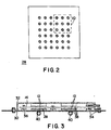
- the coaxial interconnection ball grid array 10 is shown integrated as part of a larger general ball grid array 28.
- high frequency signal generation, signal reception and digital processing can be combined in a single electronic component, such as a circuit board 14.
- Implementation of the coaxial interconnection ball grid array 10 is not limited to the specific location illustrated in FIG. 2. Rather, the position of the coaxial interconnection ball grid array 10 can be anywhere within the general ball grid array and is generally dictated by the coaxial requirements of the circuit board 14 and IMA module 12 and the geometrical array requirements of the present invention. Additionally, more than one coaxial interconnection ball grid array 10 can be implemented within the general ball grid array 28, thereby facilitating the typical multiple coaxial line requirements of conventional and newly developed IMA modules 12.
- Each portion of the general ball grid array 28 utilized as a coaxial interface would comprise a three-by-three array of solder balls 16, 20 and 22 as illustrated in FIG. 1 and described above.
- the remainder of the general ball grid array 28 may be utilized as connectors or direct interfaces between the circuit board 14, IMA modules 12 and/or other components.
- High frequency signal generation, signal reception and digital processing can thus be combined in a single circuit board 14 utilizing BGA packaging adapted to receive high frequency signals from a coaxial connection.
- the coaxial interconnection ball grid array 10 is implemented as part of a general ball grid array 28 and without the interconnection between the IMA module 12 and the circuit board 14 is generally indistinguishable from the other balls in the general ball grid array 28, manufacturing is economical and simple.
- the coaxial interconnection ball grid array 10 of the present invention is integrated as part of a larger pin grid array 28 on a circuit board 14 which is suspended between a radiator panel 30 and a radiation shield 32.
- the circuit board 14 is conventionally mounted by fasteners 34 on raised standoffs or posts 36 integral with the radiator panel 30. Other fasteners 34 are used to secure the radiation shield 32 to the radiator panel 30.
- Integrated circuit chips and/or chip packages 12, such as a high frequency IMA 12 with coaxial interface, are mounted above and beneath the circuit board 14.
- Thermally conductive adhesive material 38 may be utilized between the chip or package 12 and the surface of the radiator panel 30.
- the chips or packages 12 are positioned directly over heat pipes 40 located on the opposite face of the radiator panel 30.
- the coaxial interconnection ball grid array 10 of the present invention is positioned between the circuit board 14 and the IMAs modules 12. High frequency signals emanating from a circuit board 14 can thus be transmitted to an IMA module 12 utilizing the coaxial interconnection ball grid array 10, thereby facilitating manufacture of highly integrated microwave networks.
- IMA modules 12 can be connected together through ⁇ smart boards ⁇ (i.e., a low-power microprocessor).
- the coaxial interconnection ball grid array 10 is generally integrated as part of a larger general ball grid array, high frequency signal generation, signal reception and digital processing can be combined in a single electronic component, such as the circuit board 14.
Landscapes
- Engineering & Computer Science (AREA)
- Microelectronics & Electronic Packaging (AREA)
- Combinations Of Printed Boards (AREA)
- Waveguides (AREA)
- Shielding Devices Or Components To Electric Or Magnetic Fields (AREA)
Abstract
Description
Claims (15)
- An apparatus for interfacing with a coaxial device having a central and ground conductor, comprising:a plurality of electrically conductive structures disposed in an array, comprising a centrally disposed structure for receiving said central conductor and a plurality of ground structures disposed about said centrally disposed structure for receiving said ground conductor.
- The apparatus claimed in claim 1, wherein said array is disposed in a second array comprising a plurality of said electrically conductive structures.
- The apparatus claimed in claim 1, wherein said central and ground electrically conductive structures are electrically conductive balls.
- The apparatus claimed in claim 1, wherein said central and ground electrically conductive structures are comprised of solder.
- The apparatus claimed in claim 1 wherein said central and ground electrically conductive structures comprise electrically conductive epoxy.
- A high frequency coaxial interconnection ball grid array for providing connection to a coaxial line having a first and second conductor, comprising:a center disposed electrically conductive ball for interfacing with said first conductor; anda plurality of outer electrically conductive balls disposed about said center disposed ball for interfacing with said second conductor.
- The coaxial interconnection ball grid array claimed in claim 6, wherein said coaxial interconnection ball grid array is disposed within a second ball grid array comprising a plurality of electrically conductive balls.
- The coaxial interconnection ball grid array claimed in claim 6, wherein said center and outer electrically conductive balls are comprised of solder.
- The apparatus claimed in claim 6 wherein said central and ground electrically conductive structures comprise electrically conductive epoxy.
- A packaging structure, comprising:a circuit board;a circuit board chip package connected to said circuit board, wherein said circuit board chip package includes at least one coaxial interface having a central and ground conductor; anda plurality of electrically conductive structures disposed in an array, comprising a centrally disposed structure for receiving said central conductor and a plurality of ground structures disposed about said centrally disposed structure for receiving said ground conductor, wherein said array is disposed between said circuit board and said circuit board chip package.
- The packaging structure claimed in claim 10, wherein said central and ground electrically conductive structures are electrically conductive balls.
- A high frequency interconnection ball grid array for coaxially interconnecting an integrated microwave assembly with a circuit board assembly, comprising:a center disposed solder ball for mating with an inner conductor of a coaxial line; anda plurality of outer disposed solder balls for mating with an outer conductor of said coaxial line.
- The interconnection ball grid array claimed in claim 12, wherein said interconnection ball grid array is disposed within a second ball grid array comprising a plurality of solder balls.
- The interconnection ball grid array claimed in claim 12, wherein said center and outer solder balls are disposed in an array configuration.
- The interconnection ball grid array claimed in claim 12, wherein said center and outer solder balls are substantially equally spaced from each other.
Applications Claiming Priority (2)
| Application Number | Priority Date | Filing Date | Title |
|---|---|---|---|
| US09/245,317 US6194669B1 (en) | 1999-02-05 | 1999-02-05 | Solder ball grid array for connecting multiple millimeter wave assemblies |
| US245317 | 1999-02-05 |
Publications (2)
| Publication Number | Publication Date |
|---|---|
| EP1026742A2 true EP1026742A2 (en) | 2000-08-09 |
| EP1026742A3 EP1026742A3 (en) | 2002-10-23 |
Family
ID=22926180
Family Applications (1)
| Application Number | Title | Priority Date | Filing Date |
|---|---|---|---|
| EP00101673A Withdrawn EP1026742A3 (en) | 1999-02-05 | 2000-02-02 | Solder ball grid array for connecting multiple millimeter wave assemblies |
Country Status (3)
| Country | Link |
|---|---|
| US (1) | US6194669B1 (en) |
| EP (1) | EP1026742A3 (en) |
| JP (1) | JP3292719B2 (en) |
Cited By (1)
| Publication number | Priority date | Publication date | Assignee | Title |
|---|---|---|---|---|
| WO2005036644A3 (en) * | 2003-10-10 | 2007-03-01 | Koninkl Philips Electronics Nv | Electronic device and carrier substrate |
Families Citing this family (18)
| Publication number | Priority date | Publication date | Assignee | Title |
|---|---|---|---|---|
| CN1089486C (en) | 1995-06-26 | 2002-08-21 | 精工爱普生株式会社 | Method for forming crystalline semiconductor film |
| JP3393469B2 (en) | 1999-07-15 | 2003-04-07 | 日本電気株式会社 | Thin film semiconductor device manufacturing method and thin film semiconductor forming apparatus |
| US6639154B1 (en) * | 2000-10-10 | 2003-10-28 | Teradyne, Inc. | Apparatus for forming a connection between a circuit board and a connector, having a signal launch |
| JP2002298940A (en) * | 2001-03-30 | 2002-10-11 | Jst Mfg Co Ltd | Electrical contacts and electrical connectors using resin solder and methods for connecting these to printed wiring boards |
| JP2002298962A (en) * | 2001-03-30 | 2002-10-11 | Jst Mfg Co Ltd | Electrical contacts and electrical connectors using resin solder and methods for connecting these to printed wiring boards |
| JP2002298995A (en) * | 2001-03-30 | 2002-10-11 | Jst Mfg Co Ltd | Coaxial cable bundling member using resin solder, coaxial cable electric connector, and method of connecting bundling member to coaxial cable or electric connector |
| JP2002298946A (en) * | 2001-03-30 | 2002-10-11 | Jst Mfg Co Ltd | Electrical connector and electrical connector using resin solder and method of connecting electric wires to these |
| JP2002298938A (en) * | 2001-03-30 | 2002-10-11 | Jst Mfg Co Ltd | Electrical connector of twisted pair cable using resin solder and method of connecting electric wire to this electrical connector |
| US6727777B2 (en) | 2001-04-16 | 2004-04-27 | Vitesse Semiconductor Corporation | Apparatus and method for angled coaxial to planar structure broadband transition |
| US6998292B2 (en) * | 2001-11-30 | 2006-02-14 | Vitesse Semiconductor Corporation | Apparatus and method for inter-chip or chip-to-substrate connection with a sub-carrier |
| JP4145879B2 (en) | 2003-05-20 | 2008-09-03 | 富士通株式会社 | Semiconductor package |
| US6768189B1 (en) * | 2003-06-04 | 2004-07-27 | Northrop Grumman Corporation | High power chip scale package |
| US6933596B2 (en) * | 2003-07-01 | 2005-08-23 | Northrop Grumman Corporation | Ultra wideband BGA |
| US20060226928A1 (en) * | 2005-04-08 | 2006-10-12 | Henning Larry C | Ball coax interconnect |
| US20070251719A1 (en) * | 2006-04-27 | 2007-11-01 | Rick Sturdivant | Selective, hermetically sealed microwave package apparatus and methods |
| US8680689B1 (en) | 2012-10-04 | 2014-03-25 | International Business Machines Corporation | Coplanar waveguide for stacked multi-chip systems |
| EP2945222A1 (en) * | 2014-05-14 | 2015-11-18 | Gapwaves AB | A microwave or millimeter wave RF part using pin grid array (PGA) and/or ball grid array (BGA) technologies |
| CN112086371B (en) * | 2020-08-19 | 2023-03-14 | 中国电子科技集团公司第二十九研究所 | Broadband radio frequency board level interconnection integration method, structure and device |
Family Cites Families (14)
| Publication number | Priority date | Publication date | Assignee | Title |
|---|---|---|---|---|
| NL7003475A (en) * | 1969-03-28 | 1970-09-30 | ||
| US4295183A (en) | 1979-06-29 | 1981-10-13 | International Business Machines Corporation | Thin film metal package for LSI chips |
| JP3014503B2 (en) * | 1991-08-05 | 2000-02-28 | 日本特殊陶業株式会社 | Package for integrated circuit |
| US5347086A (en) * | 1992-03-24 | 1994-09-13 | Microelectronics And Computer Technology Corporation | Coaxial die and substrate bumps |
| EP0604005A1 (en) * | 1992-10-26 | 1994-06-29 | Texas Instruments Incorporated | Device packaged in a high interconnect density land grid array package having electrical and optical interconnects |
| US5376584A (en) | 1992-12-31 | 1994-12-27 | International Business Machines Corporation | Process of making pad structure for solder ball limiting metallurgy having reduced edge stress |
| US5401912A (en) * | 1993-06-07 | 1995-03-28 | St Microwave Corp., Arizona Operations | Microwave surface mount package |
| US5456004A (en) | 1994-01-04 | 1995-10-10 | Dell Usa, L.P. | Anisotropic interconnect methodology for cost effective manufacture of high density printed circuit boards |
| US5593082A (en) | 1994-11-15 | 1997-01-14 | Tosoh Smd, Inc. | Methods of bonding targets to backing plate members using solder pastes and target/backing plate assemblies bonded thereby |
| JP3473923B2 (en) * | 1995-02-27 | 2003-12-08 | 新光電気工業株式会社 | BGA package and mounting structure of the package |
| SE9502326D0 (en) * | 1995-06-27 | 1995-06-27 | Sivers Ima Ab | Microwave circuit, such circuit of nested embodiment, and use of the microwave circuit in a circuit arrangement |
| JP4195731B2 (en) * | 1996-07-25 | 2008-12-10 | 富士通株式会社 | Multilayer printed board and high frequency circuit device using the same |
| JPH10178144A (en) * | 1996-12-19 | 1998-06-30 | Fujitsu Ltd | Coaxial electrode structure of BGA type electronic components |
| JP3150108B2 (en) | 1998-10-09 | 2001-03-26 | 埼玉日本電気株式会社 | Mounting structure of ball grid array package |
-
1999
- 1999-02-05 US US09/245,317 patent/US6194669B1/en not_active Expired - Lifetime
-
2000
- 2000-02-02 EP EP00101673A patent/EP1026742A3/en not_active Withdrawn
- 2000-02-07 JP JP2000028600A patent/JP3292719B2/en not_active Expired - Fee Related
Cited By (2)
| Publication number | Priority date | Publication date | Assignee | Title |
|---|---|---|---|---|
| WO2005036644A3 (en) * | 2003-10-10 | 2007-03-01 | Koninkl Philips Electronics Nv | Electronic device and carrier substrate |
| CN101142676B (en) * | 2003-10-10 | 2010-07-14 | 台湾积体电路制造股份有限公司 | Electronic devices and carrier substrates |
Also Published As
| Publication number | Publication date |
|---|---|
| JP3292719B2 (en) | 2002-06-17 |
| US6194669B1 (en) | 2001-02-27 |
| EP1026742A3 (en) | 2002-10-23 |
| JP2000232197A (en) | 2000-08-22 |
Similar Documents
| Publication | Publication Date | Title |
|---|---|---|
| US6194669B1 (en) | Solder ball grid array for connecting multiple millimeter wave assemblies | |
| US6137693A (en) | High-frequency electronic package with arbitrarily-shaped interconnects and integral shielding | |
| US5675302A (en) | Microwave compression interconnect using dielectric filled three-wire line with compressible conductors | |
| KR100511814B1 (en) | Low cost, large scale rf hybrid package for simple assembly onto mixed signal printed wiring boards | |
| EP0731525B1 (en) | Three-wire-line vertical interconnect structure for multilevel substrates | |
| EP4016620A1 (en) | Package with an integrated circuit die and a waveguide launcher | |
| US6911734B2 (en) | Semiconductor device and electronic device | |
| US20030068920A1 (en) | High density, high frequency memory chip modules having thermal management structures | |
| US20060226928A1 (en) | Ball coax interconnect | |
| CN118919495A (en) | AIP airtight packaging structure based on LTCC packaging substrate and antenna wiring cover plate | |
| US20040266224A1 (en) | Active configurable and stackable interface connector | |
| EP4150704B1 (en) | Reactive array | |
| WO2000004595A2 (en) | Land-side mounting of components to an integrated circuit package | |
| EP4557504A1 (en) | Pitch-reducing solder interconnect for rf transitions | |
| CN120048815B (en) | Chip packaging transition structure, integrated antenna module and communication equipment | |
| US12451579B2 (en) | Interposers with millimeter-wave transitions | |
| US12451578B2 (en) | Interposers with millimeter-wave coaxial-to-waveguide transistions | |
| JP7560224B2 (en) | PCB Cavity Mode Suppression | |
| JP7660364B2 (en) | Wireless communication module | |
| WO2025151071A1 (en) | Integrated circuit package | |
| JPH10125731A (en) | Semiconductor integrated circuit device and method of manufacturing the same |
Legal Events
| Date | Code | Title | Description |
|---|---|---|---|
| PUAI | Public reference made under article 153(3) epc to a published international application that has entered the european phase |
Free format text: ORIGINAL CODE: 0009012 |
|
| AK | Designated contracting states |
Kind code of ref document: A2 Designated state(s): AT BE CH CY DE DK ES FI FR GB GR IE IT LI LU MC NL PT SE |
|
| AX | Request for extension of the european patent |
Free format text: AL;LT;LV;MK;RO;SI |
|
| RIN1 | Information on inventor provided before grant (corrected) |
Inventor name: DAVIDHEISER, ROGER A. Inventor name: BJORNDAHL, WILLIAM D. Inventor name: STONES, D. IAN Inventor name: SELK, KENNETH C. Inventor name: LEE, ALFRED E. |
|
| PUAL | Search report despatched |
Free format text: ORIGINAL CODE: 0009013 |
|
| AK | Designated contracting states |
Kind code of ref document: A3 Designated state(s): AT BE CH CY DE DK ES FI FR GB GR IE IT LI LU MC NL PT SE |
|
| AX | Request for extension of the european patent |
Free format text: AL;LT;LV;MK;RO;SI |
|
| 17P | Request for examination filed |
Effective date: 20030401 |
|
| AKX | Designation fees paid |
Designated state(s): DE FR GB IT |
|
| RAP1 | Party data changed (applicant data changed or rights of an application transferred) |
Owner name: NORTHROP GRUMMAN CORPORATION |
|
| RAP1 | Party data changed (applicant data changed or rights of an application transferred) |
Owner name: NORTHROP GRUMMAN CORPORATION |
|
| 17Q | First examination report despatched |
Effective date: 20071031 |
|
| STAA | Information on the status of an ep patent application or granted ep patent |
Free format text: STATUS: THE APPLICATION IS DEEMED TO BE WITHDRAWN |
|
| 18D | Application deemed to be withdrawn |
Effective date: 20080311 |