EP1026738A2 - Novel mixed voltage CMOS process for high reliability and high performance core and I/O transistors with reduced mask steps - Google Patents
Novel mixed voltage CMOS process for high reliability and high performance core and I/O transistors with reduced mask steps Download PDFInfo
- Publication number
- EP1026738A2 EP1026738A2 EP00300969A EP00300969A EP1026738A2 EP 1026738 A2 EP1026738 A2 EP 1026738A2 EP 00300969 A EP00300969 A EP 00300969A EP 00300969 A EP00300969 A EP 00300969A EP 1026738 A2 EP1026738 A2 EP 1026738A2
- Authority
- EP
- European Patent Office
- Prior art keywords
- doped region
- semiconductor body
- gate stack
- transistor
- conductivity type
- Prior art date
- Legal status (The legal status is an assumption and is not a legal conclusion. Google has not performed a legal analysis and makes no representation as to the accuracy of the status listed.)
- Granted
Links
Images


Classifications
-
- H—ELECTRICITY
- H10—SEMICONDUCTOR DEVICES; ELECTRIC SOLID-STATE DEVICES NOT OTHERWISE PROVIDED FOR
- H10D—INORGANIC ELECTRIC SEMICONDUCTOR DEVICES
- H10D84/00—Integrated devices formed in or on semiconductor substrates that comprise only semiconducting layers, e.g. on Si wafers or on GaAs-on-Si wafers
- H10D84/01—Manufacture or treatment
- H10D84/0123—Integrating together multiple components covered by H10D12/00 or H10D30/00, e.g. integrating multiple IGBTs
- H10D84/0126—Integrating together multiple components covered by H10D12/00 or H10D30/00, e.g. integrating multiple IGBTs the components including insulated gates, e.g. IGFETs
- H10D84/0165—Integrating together multiple components covered by H10D12/00 or H10D30/00, e.g. integrating multiple IGBTs the components including insulated gates, e.g. IGFETs the components including complementary IGFETs, e.g. CMOS devices
- H10D84/017—Manufacturing their source or drain regions, e.g. silicided source or drain regions
-
- H—ELECTRICITY
- H10—SEMICONDUCTOR DEVICES; ELECTRIC SOLID-STATE DEVICES NOT OTHERWISE PROVIDED FOR
- H10D—INORGANIC ELECTRIC SEMICONDUCTOR DEVICES
- H10D84/00—Integrated devices formed in or on semiconductor substrates that comprise only semiconducting layers, e.g. on Si wafers or on GaAs-on-Si wafers
- H10D84/01—Manufacture or treatment
- H10D84/0123—Integrating together multiple components covered by H10D12/00 or H10D30/00, e.g. integrating multiple IGBTs
- H10D84/0126—Integrating together multiple components covered by H10D12/00 or H10D30/00, e.g. integrating multiple IGBTs the components including insulated gates, e.g. IGFETs
- H10D84/0165—Integrating together multiple components covered by H10D12/00 or H10D30/00, e.g. integrating multiple IGBTs the components including insulated gates, e.g. IGFETs the components including complementary IGFETs, e.g. CMOS devices
- H10D84/0181—Manufacturing their gate insulating layers
-
- H—ELECTRICITY
- H10—SEMICONDUCTOR DEVICES; ELECTRIC SOLID-STATE DEVICES NOT OTHERWISE PROVIDED FOR
- H10D—INORGANIC ELECTRIC SEMICONDUCTOR DEVICES
- H10D84/00—Integrated devices formed in or on semiconductor substrates that comprise only semiconducting layers, e.g. on Si wafers or on GaAs-on-Si wafers
- H10D84/01—Manufacture or treatment
- H10D84/02—Manufacture or treatment characterised by using material-based technologies
- H10D84/03—Manufacture or treatment characterised by using material-based technologies using Group IV technology, e.g. silicon technology or silicon-carbide [SiC] technology
- H10D84/038—Manufacture or treatment characterised by using material-based technologies using Group IV technology, e.g. silicon technology or silicon-carbide [SiC] technology using silicon technology, e.g. SiGe
Definitions
- the instant invention is a mixed voltage CMOS method for high reliability and high performance core and input-output transistors with reduced masks.
- the method includes the steps of:
- the method of the instant invention will result in the following key features of the core NMOS transistor and the I/O NMOS transistor;
- this silicon-containing material is comprised of polycrystalline silicon("poly” or “polysilicon"), but it may be comprised of epitaxial silicon or any other semiconducting material.
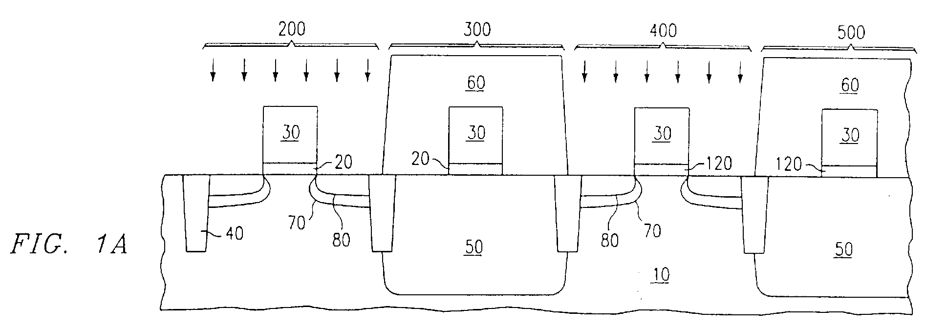
- Contained in the substrate will be isolation structures 40. These isolation structures may comprise an oxide or some other insulator. The purpose of the isolation structure 40 is to isolate the actives devices from one another on the substrate.
- the substrate will contain wells 50 that will be of the opposite conductivity type when compared to the conductivity of the substrate.
- the substrate 10 is p-type and the well 50 is n-type.
- the core NMOS transistor will be fabricated in region 200, the core PMOS transistor in region 300, the I/O NMOS transistor in region 400, and the I/O PMOS transistor in region 500,
- the gate dielectric for the I/O transistors 120 will be thicker than the gate dielectric 20 for the core transistors.
- a layer of photoresist is formed over the substrate 10. Using standard photolithographic techniques, the resist is patterned and etched to produce the areas of resist 60 that cover the PMOS core and I/O transistor.
- a blanket pocket p-type implant followed by a blanket n-type LDD implant is performed resulting in the p-type doping profile 70, and the n-type doping profile 80.
- pocket implants refer to an implant that is used to reduce the effect of the short transistor gate length on transistor properties such as threshold voltage. The effect of the pocket implant is not however limited to threshold voltage.
- the pocket implant for a particular transistor type usually results in a doping profile that extends beyond the drain extension of the transistor.
- the species of the p-type pocket implant can consist of B, BF2, Ga, In, or any other suitable p-type dopant.
- the species of the n-type LDD implant can consist of As, P, Sb, or any other suitable n-type dopant.
- a layer of photoresist is formed on the substrate 10, patterned and etched to form the structure 150 which covers the NMOS core transistor.
- a blanket pocket n-type implant followed by a blanket p-type LDD implant is performed resulting in the n-type doping profile 90, and the p-type doping profile 100.
- the species of the n-type pocket implant can consist of As, P, Sb or any other suitable n-type dopant.
- the species of the p-type LDD implant can consist of B, BF2, Ga, In, or any other suitable p-type dopant.
- the order of the implants is somewhat arbitrary and the LDD implant could be performed before the pocket implant. After completion of the implants the integrated circuit is completed using standard CMOS processing techniques.
Landscapes
- Metal-Oxide And Bipolar Metal-Oxide Semiconductor Integrated Circuits (AREA)
- Insulated Gate Type Field-Effect Transistor (AREA)
Abstract
Description
| Implant | Condition | Species |
| NMOS-LDD | 1.2x1015cm-2,15keV | As |
| NMOS-pocket | 2.4x1013cm-2, 15keV | B |
| PMOS-LDD | 4x1014cm-2, 10keV | BF2 |
| PMOS-pocket | 3.2x1013cm-2, 60keV | P |
Claims (10)
- A method of fabricating a mixed voltage integrated circuit including the steps of:forming a gate dielectric layer on a semiconductor body of a first conductivity type,forming a conductive layer on the gate dielectric layer,forming a transistor gate stack on the semiconductor body by etching the gate dielectric layer and the conductive layer,forming a first doped region of the first conductivity type, below the surface of the semiconductor body adjacent to the transistor gate stack, by implanting a first dopant into the semiconductor body adjacent to the transistor gate stack andforming a second doped region of conductivity type opposite to the first conductivity type, between the surface of the semiconductor body and where the first doped region has been or will be implanted , by implanting a second dopant into the semiconductor body adjacent to the transistor gate stack,both the first doped region and the second doped region being separated into two parts which are so positioned in relation to the transistor gate stack as to be capable of functioning as transistor source and drain regions.
- A method as claimed in claim 1, including the steps of:forming a third doped region of conductivity type opposite to the first conductivity type, at a depth below the surface of the semiconductor body which places the first doped region between the second and third doped regions, by implanting a third dopant into the semiconductor body adjacent to the transistor gate stack andforming a fourth doped region of the first conductivity type, between the surface of the semiconductor body and the second doped region, by implanting a fourth dopant into the semiconductor body adjacent to the transistor gate stack,both the third doped region and the fourth doped region being separated into two parts which are so positioned in relation to the transistor gate stack as to be capable of functioning as elements of the transistor source and drain regions.
- A method as claimed in claim 1 or claim 2, including the step of forming the semiconductor body as a well in a semiconductor substrate.
- A method as claimed in claim 1, repeated to form a plurality of transistor gate stacks on the semiconductor body and a plurality of respective first and second doped regions, in the semiconductor body, associated with the transistor gate stacks.
- A method as claimed in claim 4, including the steps of:forming a third doped region of conductivity type opposite to the first conductivity type, at a depth below the surface of the semiconductor body which places a selected first doped region between the associated second and third doped regions, by implanting a third dopant into the semiconductor body adjacent to the transistor gate stack with which the selected first doped region is associated andforming a fourth doped region of the first conductivity type, between the surface of the semiconductor body and the second doped region associated with the selected first doped region, by implanting a fourth dopant into the semiconductor body adjacent to the transistor gate stack with which the selected first doped region is associated,both the third doped region and the fourth doped region being separated into two parts so positioned in relation to the transistor gate stack with which the selected first doped region is associated as to be capable of functioning as elements of the transistor source and drain regions.
- A method as claimed in claim 1, repeated to form a first transistor gate stack on a first transistor body of a first conductivity type and a second transistor gate stack on a second semiconductor body of a conductivity type opposite the first conductivity type, the second semiconductor body being in the form of a well in the first semiconductor body and the dielectric layer of the second transistor gate stack is thicker than the dielectric layer of the first transistor gate stack.
- A method as claimed in any one of claims 1 to 6, wherein the gate dielectric layer is of a material selected from the group consisting of: silicon dioxide, silicon oxynitride, silicon nitride and any combination thereof.
- A method as claimed in any one of claims 1 to 7, wherein the conductive layer is of a material selected from the group consisting of: doped polysilicon, undoped polysilicon, epitaxial silicon and any combination thereof.
- A method as claimed in any one of claims 1 to 8, wherein the first conductivity type is p-type conductivity and p-type conductivity regions are implanted with a dopant selected from the group consisting of: B, BF2, Ga, In and any combination thereof.
- A method as claimed in any one of claims 1 to 8, wherein the first conductivity type is n-type conductivity and n-type conductivity regions are implanted with a dopant selected from the group consisting of: As, P, Sb and any combination thereof.
Applications Claiming Priority (2)
| Application Number | Priority Date | Filing Date | Title |
|---|---|---|---|
| US11897999P | 1999-02-08 | 1999-02-08 | |
| US118979P | 1999-02-08 |
Publications (3)
| Publication Number | Publication Date |
|---|---|
| EP1026738A2 true EP1026738A2 (en) | 2000-08-09 |
| EP1026738A3 EP1026738A3 (en) | 2004-06-23 |
| EP1026738B1 EP1026738B1 (en) | 2006-06-21 |
Family
ID=22381923
Family Applications (1)
| Application Number | Title | Priority Date | Filing Date |
|---|---|---|---|
| EP00300969A Expired - Lifetime EP1026738B1 (en) | 1999-02-08 | 2000-02-08 | Novel mixed voltage CMOS process for high reliability and high performance core and I/O transistors with reduced mask steps |
Country Status (6)
| Country | Link |
|---|---|
| US (1) | US6258644B1 (en) |
| EP (1) | EP1026738B1 (en) |
| JP (1) | JP2000232167A (en) |
| KR (1) | KR20000071335A (en) |
| DE (1) | DE60028847T2 (en) |
| TW (1) | TW459291B (en) |
Cited By (1)
| Publication number | Priority date | Publication date | Assignee | Title |
|---|---|---|---|---|
| EP3340290A1 (en) * | 2016-12-22 | 2018-06-27 | Semiconductor Manufacturing International Corporation (Shanghai) | Semiconductor device and fabrication method thereof |
Families Citing this family (18)
| Publication number | Priority date | Publication date | Assignee | Title |
|---|---|---|---|---|
| US6166417A (en) * | 1998-06-30 | 2000-12-26 | Intel Corporation | Complementary metal gates and a process for implementation |
| US6878968B1 (en) * | 1999-05-10 | 2005-04-12 | Semiconductor Energy Laboratory Co., Ltd. | Semiconductor device |
| JP2001127171A (en) * | 1999-10-26 | 2001-05-11 | Matsushita Electronics Industry Corp | Semiconductor device and manufacturing method thereof |
| US6479339B2 (en) * | 2000-10-10 | 2002-11-12 | Texas Instruments Incorporated | Use of a thin nitride spacer in a split gate embedded analog process |
| US6541819B2 (en) * | 2001-05-24 | 2003-04-01 | Agere Systems Inc. | Semiconductor device having non-power enhanced and power enhanced metal oxide semiconductor devices and a method of manufacture therefor |
| JP4665141B2 (en) * | 2001-06-29 | 2011-04-06 | 富士通セミコンダクター株式会社 | Semiconductor device and manufacturing method thereof |
| JP3426587B2 (en) | 2001-07-06 | 2003-07-14 | 沖電気工業株式会社 | Semiconductor device and manufacturing method thereof |
| JP5073136B2 (en) * | 2001-08-24 | 2012-11-14 | ルネサスエレクトロニクス株式会社 | Semiconductor device |
| KR100450666B1 (en) * | 2001-09-03 | 2004-10-01 | 삼성전자주식회사 | Method of forming selectively metal silicide layer and semiconductor device having the same |
| US6482703B1 (en) * | 2001-09-28 | 2002-11-19 | Taiwan Semiconductor Manufacturing Company | Method for fabricating an electrostatic discharge device in a dual gate oxide process |
| US7585763B2 (en) * | 2005-11-07 | 2009-09-08 | Samsung Electronics Co., Ltd. | Methods of fabricating integrated circuit devices using anti-reflective coating as implant blocking layer |
| US7557022B2 (en) * | 2006-06-13 | 2009-07-07 | Texas Instruments Incorporated | Implantation of carbon and/or fluorine in NMOS fabrication |
| KR100808797B1 (en) * | 2006-08-29 | 2008-03-03 | 동부일렉트로닉스 주식회사 | Ion Implantation Method of Semiconductor Device |
| KR100857453B1 (en) * | 2006-09-29 | 2008-09-08 | 한국전자통신연구원 | Photosensitive pixels in low voltage image sensor |
| US7879639B2 (en) * | 2007-04-13 | 2011-02-01 | Taiwan Semiconductor Manufacturing Company, Ltd. | Method and device to reduce dark current in image sensors |
| FR2939962B1 (en) | 2008-12-15 | 2011-03-18 | Soitec Silicon On Insulator | METHOD OF SLURING A STRUCTURE |
| JP5672055B2 (en) * | 2011-02-23 | 2015-02-18 | 富士通セミコンダクター株式会社 | Manufacturing method of semiconductor device |
| CN111370372B (en) * | 2020-04-22 | 2024-01-19 | 上海华虹宏力半导体制造有限公司 | How to make CMOS integrated devices |
Family Cites Families (7)
| Publication number | Priority date | Publication date | Assignee | Title |
|---|---|---|---|---|
| US5894158A (en) * | 1991-09-30 | 1999-04-13 | Stmicroelectronics, Inc. | Having halo regions integrated circuit device structure |
| US5364810A (en) * | 1992-07-28 | 1994-11-15 | Motorola, Inc. | Methods of forming a vertical field-effect transistor and a semiconductor memory cell |
| FR2700418B1 (en) * | 1993-01-12 | 1995-04-07 | France Telecom | Electronic component capable of negative dynamic resistance and corresponding manufacturing process. |
| JP3227983B2 (en) * | 1993-09-10 | 2001-11-12 | ソニー株式会社 | Semiconductor device and manufacturing method thereof |
| US5480828A (en) * | 1994-09-30 | 1996-01-02 | Taiwan Semiconductor Manufacturing Corp. Ltd. | Differential gate oxide process by depressing or enhancing oxidation rate for mixed 3/5 V CMOS process |
| US5780897A (en) * | 1995-11-13 | 1998-07-14 | Digital Equipment Corporation | ESD protection clamp for mixed voltage I/O stages using NMOS transistors |
| US6075271A (en) * | 1998-03-03 | 2000-06-13 | Motorola, Inc. | Semiconductor device inhibiting parasitic effects during electrostatic discharge |
-
2000
- 2000-02-08 JP JP2000030167A patent/JP2000232167A/en not_active Abandoned
- 2000-02-08 KR KR1020000005722A patent/KR20000071335A/en not_active Withdrawn
- 2000-02-08 DE DE60028847T patent/DE60028847T2/en not_active Expired - Lifetime
- 2000-02-08 EP EP00300969A patent/EP1026738B1/en not_active Expired - Lifetime
- 2000-02-08 US US09/499,719 patent/US6258644B1/en not_active Expired - Lifetime
- 2000-03-09 TW TW089101872A patent/TW459291B/en not_active IP Right Cessation
Cited By (5)
| Publication number | Priority date | Publication date | Assignee | Title |
|---|---|---|---|---|
| EP3340290A1 (en) * | 2016-12-22 | 2018-06-27 | Semiconductor Manufacturing International Corporation (Shanghai) | Semiconductor device and fabrication method thereof |
| US20180182626A1 (en) * | 2016-12-22 | 2018-06-28 | Semiconductor Manufacturing International (Shanghai) Corporation | Semiconductor device and fabrication method thereof |
| CN108231682A (en) * | 2016-12-22 | 2018-06-29 | 中芯国际集成电路制造(上海)有限公司 | Semiconductor devices and forming method thereof |
| US10727130B2 (en) * | 2016-12-22 | 2020-07-28 | Semiconductor Manufacturing International (Shanghai) Corporation | Semiconductor device and fabrication method thereof |
| CN108231682B (en) * | 2016-12-22 | 2021-02-02 | 中芯国际集成电路制造(上海)有限公司 | Semiconductor device and method of forming the same |
Also Published As
| Publication number | Publication date |
|---|---|
| DE60028847T2 (en) | 2006-12-07 |
| US6258644B1 (en) | 2001-07-10 |
| DE60028847D1 (en) | 2006-08-03 |
| KR20000071335A (en) | 2000-11-25 |
| EP1026738B1 (en) | 2006-06-21 |
| JP2000232167A (en) | 2000-08-22 |
| TW459291B (en) | 2001-10-11 |
| EP1026738A3 (en) | 2004-06-23 |
Similar Documents
| Publication | Publication Date | Title |
|---|---|---|
| US6548874B1 (en) | Higher voltage transistors for sub micron CMOS processes | |
| US6514810B1 (en) | Buried channel PMOS transistor in dual gate CMOS with reduced masking steps | |
| US6153455A (en) | Method of fabricating ultra shallow junction CMOS transistors with nitride disposable spacer | |
| EP1026738B1 (en) | Novel mixed voltage CMOS process for high reliability and high performance core and I/O transistors with reduced mask steps | |
| US6316302B1 (en) | Isotropically etching sidewall spacers to be used for both an NMOS source/drain implant and a PMOS LDD implant | |
| US4435895A (en) | Process for forming complementary integrated circuit devices | |
| US6660603B2 (en) | Higher voltage drain extended MOS transistors with self-aligned channel and drain extensions | |
| US5427964A (en) | Insulated gate field effect transistor and method for fabricating | |
| JP2002033396A (en) | Method for manufacturing high performance, high reliability input / output device and analog compatible input / output and core device using core device injection | |
| WO1998008253A1 (en) | Dual gate oxide thickness integrated circuit and process for making same | |
| US6479339B2 (en) | Use of a thin nitride spacer in a split gate embedded analog process | |
| KR100823821B1 (en) | Manufacturing Method of Semiconductor Integrated Circuit Device | |
| EP0676798A2 (en) | Insulated gate field effect transistor with assymetric channel and method for fabricating | |
| US20030127694A1 (en) | Higher voltage transistors for sub micron CMOS processes | |
| US6908800B1 (en) | Tunable sidewall spacer process for CMOS integrated circuits | |
| US6583013B1 (en) | Method for forming a mixed voltage circuit having complementary devices | |
| US6303420B1 (en) | Integrated bipolar junction transistor for mixed signal circuits | |
| JP4501183B2 (en) | Manufacturing method of semiconductor device | |
| US6743679B2 (en) | Integrated circuit devices with high and low voltage components and processes for manufacturing these devices | |
| US5804497A (en) | Selectively doped channel region for increased IDsat and method for making same | |
| US7560779B2 (en) | Method for forming a mixed voltage circuit having complementary devices | |
| KR100281397B1 (en) | A method of forming an ultra-thin soi electrostatic discharge protection device | |
| KR100632068B1 (en) | Manufacturing method of MOS transistor of semiconductor device | |
| US7553718B2 (en) | Methods, systems and structures for forming semiconductor structures incorporating high-temperature processing steps | |
| US6448121B1 (en) | High threshold PMOS transistor in a surface-channel process |
Legal Events
| Date | Code | Title | Description |
|---|---|---|---|
| PUAI | Public reference made under article 153(3) epc to a published international application that has entered the european phase |
Free format text: ORIGINAL CODE: 0009012 |
|
| AK | Designated contracting states |
Kind code of ref document: A2 Designated state(s): AT BE CH CY DE DK ES FI FR GB GR IE IT LI LU MC NL PT SE |
|
| AX | Request for extension of the european patent |
Free format text: AL;LT;LV;MK;RO;SI |
|
| RIN1 | Information on inventor provided before grant (corrected) |
Inventor name: MEHROTRA, MANOJ Inventor name: NANDAKUMAR, MAHALINGAM Inventor name: RODDER, MARK S. |
|
| PUAL | Search report despatched |
Free format text: ORIGINAL CODE: 0009013 |
|
| AK | Designated contracting states |
Kind code of ref document: A3 Designated state(s): AT BE CH CY DE DK ES FI FR GB GR IE IT LI LU MC NL PT SE |
|
| AX | Request for extension of the european patent |
Extension state: AL LT LV MK RO SI |
|
| 17P | Request for examination filed |
Effective date: 20041209 |
|
| AKX | Designation fees paid |
Designated state(s): DE FR GB |
|
| 17Q | First examination report despatched |
Effective date: 20050309 |
|
| GRAP | Despatch of communication of intention to grant a patent |
Free format text: ORIGINAL CODE: EPIDOSNIGR1 |
|
| RIN1 | Information on inventor provided before grant (corrected) |
Inventor name: NANDAKUMAR, MAHALINGAM Inventor name: MEHROTRA, MANOJ Inventor name: RODDER, MARK S. |
|
| GRAS | Grant fee paid |
Free format text: ORIGINAL CODE: EPIDOSNIGR3 |
|
| GRAA | (expected) grant |
Free format text: ORIGINAL CODE: 0009210 |
|
| AK | Designated contracting states |
Kind code of ref document: B1 Designated state(s): DE FR GB |
|
| REG | Reference to a national code |
Ref country code: GB Ref legal event code: FG4D |
|
| RIN1 | Information on inventor provided before grant (corrected) |
Inventor name: NANDAKUMAR, MAHALINGAM Inventor name: RODDER, MARK S. Inventor name: MEHROTRA, MANOJ |
|
| REF | Corresponds to: |
Ref document number: 60028847 Country of ref document: DE Date of ref document: 20060803 Kind code of ref document: P |
|
| PLBE | No opposition filed within time limit |
Free format text: ORIGINAL CODE: 0009261 |
|
| STAA | Information on the status of an ep patent application or granted ep patent |
Free format text: STATUS: NO OPPOSITION FILED WITHIN TIME LIMIT |
|
| EN | Fr: translation not filed | ||
| 26N | No opposition filed |
Effective date: 20070322 |
|
| PG25 | Lapsed in a contracting state [announced via postgrant information from national office to epo] |
Ref country code: FR Free format text: LAPSE BECAUSE OF FAILURE TO SUBMIT A TRANSLATION OF THE DESCRIPTION OR TO PAY THE FEE WITHIN THE PRESCRIBED TIME-LIMIT Effective date: 20070309 |
|
| PG25 | Lapsed in a contracting state [announced via postgrant information from national office to epo] |
Ref country code: FR Free format text: LAPSE BECAUSE OF FAILURE TO SUBMIT A TRANSLATION OF THE DESCRIPTION OR TO PAY THE FEE WITHIN THE PRESCRIBED TIME-LIMIT Effective date: 20060621 |
|
| PGFP | Annual fee paid to national office [announced via postgrant information from national office to epo] |
Ref country code: DE Payment date: 20150227 Year of fee payment: 16 |
|
| PGFP | Annual fee paid to national office [announced via postgrant information from national office to epo] |
Ref country code: GB Payment date: 20150126 Year of fee payment: 16 |
|
| REG | Reference to a national code |
Ref country code: DE Ref legal event code: R119 Ref document number: 60028847 Country of ref document: DE |
|
| GBPC | Gb: european patent ceased through non-payment of renewal fee |
Effective date: 20160208 |
|
| PG25 | Lapsed in a contracting state [announced via postgrant information from national office to epo] |
Ref country code: DE Free format text: LAPSE BECAUSE OF NON-PAYMENT OF DUE FEES Effective date: 20160901 Ref country code: GB Free format text: LAPSE BECAUSE OF NON-PAYMENT OF DUE FEES Effective date: 20160208 |