EP1026548A2 - Optical member for photolithography and photolithography apparatus - Google Patents
Optical member for photolithography and photolithography apparatus Download PDFInfo
- Publication number
- EP1026548A2 EP1026548A2 EP00102108A EP00102108A EP1026548A2 EP 1026548 A2 EP1026548 A2 EP 1026548A2 EP 00102108 A EP00102108 A EP 00102108A EP 00102108 A EP00102108 A EP 00102108A EP 1026548 A2 EP1026548 A2 EP 1026548A2
- Authority
- EP
- European Patent Office
- Prior art keywords
- light
- optical
- calcium fluoride
- optical system
- transmittance
- Prior art date
- Legal status (The legal status is an assumption and is not a legal conclusion. Google has not performed a legal analysis and makes no representation as to the accuracy of the status listed.)
- Withdrawn
Links
Images




Classifications
-
- G—PHYSICS
- G03—PHOTOGRAPHY; CINEMATOGRAPHY; ANALOGOUS TECHNIQUES USING WAVES OTHER THAN OPTICAL WAVES; ELECTROGRAPHY; HOLOGRAPHY
- G03F—PHOTOMECHANICAL PRODUCTION OF TEXTURED OR PATTERNED SURFACES, e.g. FOR PRINTING, FOR PROCESSING OF SEMICONDUCTOR DEVICES; MATERIALS THEREFOR; ORIGINALS THEREFOR; APPARATUS SPECIALLY ADAPTED THEREFOR
- G03F7/00—Photomechanical, e.g. photolithographic, production of textured or patterned surfaces, e.g. printing surfaces; Materials therefor, e.g. comprising photoresists; Apparatus specially adapted therefor
- G03F7/70—Microphotolithographic exposure; Apparatus therefor
- G03F7/70058—Mask illumination systems
-
- G—PHYSICS
- G03—PHOTOGRAPHY; CINEMATOGRAPHY; ANALOGOUS TECHNIQUES USING WAVES OTHER THAN OPTICAL WAVES; ELECTROGRAPHY; HOLOGRAPHY
- G03F—PHOTOMECHANICAL PRODUCTION OF TEXTURED OR PATTERNED SURFACES, e.g. FOR PRINTING, FOR PROCESSING OF SEMICONDUCTOR DEVICES; MATERIALS THEREFOR; ORIGINALS THEREFOR; APPARATUS SPECIALLY ADAPTED THEREFOR
- G03F7/00—Photomechanical, e.g. photolithographic, production of textured or patterned surfaces, e.g. printing surfaces; Materials therefor, e.g. comprising photoresists; Apparatus specially adapted therefor
- G03F7/70—Microphotolithographic exposure; Apparatus therefor
- G03F7/70216—Mask projection systems
- G03F7/70241—Optical aspects of refractive lens systems, i.e. comprising only refractive elements
-
- G—PHYSICS
- G03—PHOTOGRAPHY; CINEMATOGRAPHY; ANALOGOUS TECHNIQUES USING WAVES OTHER THAN OPTICAL WAVES; ELECTROGRAPHY; HOLOGRAPHY
- G03F—PHOTOMECHANICAL PRODUCTION OF TEXTURED OR PATTERNED SURFACES, e.g. FOR PRINTING, FOR PROCESSING OF SEMICONDUCTOR DEVICES; MATERIALS THEREFOR; ORIGINALS THEREFOR; APPARATUS SPECIALLY ADAPTED THEREFOR
- G03F7/00—Photomechanical, e.g. photolithographic, production of textured or patterned surfaces, e.g. printing surfaces; Materials therefor, e.g. comprising photoresists; Apparatus specially adapted therefor
- G03F7/70—Microphotolithographic exposure; Apparatus therefor
- G03F7/70483—Information management; Active and passive control; Testing; Wafer monitoring, e.g. pattern monitoring
- G03F7/70591—Testing optical components
Definitions
- the present invention relates to an optical member for photolithography made of a calcium fluoride crystal, and a photolithography apparatus using this optical member; and, more specifically, to an optical member made of a calcium fluoride crystal which is employed in a stepper or scanner which is a photolithography apparatus using, for its exposure light source, an F 2 laser (157 nm), an ArCl excimer laser (175 nm), a Kr 2 excimer laser (146 nm), an Ar 2 excimer laser (126 nm), a solid-state laser utilizing a nonlinear optical effect, or other ultraviolet rays, and a photolithography apparatus using this optical member.
- a stepper or scanner which is a photolithography apparatus using, for its exposure light source, an F 2 laser (157 nm), an ArCl excimer laser (175 nm), a Kr 2 excimer laser (146 nm), an Ar 2 excimer laser (126 nm), a solid-state laser utilizing a nonline
- optical members are often designed by use of two kinds of materials constituted by a calcium fluoride crystal and silica glass in general.
- Bridgman-Stockbarger method crucible descending method
- Czochralski method Czochralski method
- Bridgman-Stockbarger method is in wide use since it is advantageous in that crystal growth is carried out while being kept from contamination from the air and in that it can make a large crystal.
- a fluorinating agent e.g., lead fluoride or the like
- scavenger a fluorinating agent known as scavenger
- the resulting mixture is sealed in a crucible and heated in a vacuum so as to be melted, and then the crucible is descended at a velocity of 0.5 to 5 mm/hour so as to effect crystal growth.
- calcium fluoride crystal is subjected to a heat treatment for eliminating thermal stress, and then is cut and processed, so as to become a material for an optical member.
- prisms, mirrors, and various lenses are manufactured as optical members for photolithography. These optical members are subjected to optical grinding with a required precision, and are formed with a required coating.
- a member used in an optical system of a photolithography apparatus absorbs light, then its influence on the whole optical system is strong even when the amount of absorption is very little. Specifically, there occurs such a problem that not only its throughput (light transmission property of the whole optical system) is unfavorable, but also light absorption causes the temperature of optical members (lenses) to rise, thereby deteriorating imaging performances. Therefore, for establishing a photolithography technique utilizing vacuum ultraviolet rays, it is very important that slight absorption in optical members be suppressed. In the optical members made of calcium fluoride crystals manufactured by conventional methods, however, it has been difficult to obtain desired optical performances.
- Japanese Patent Application Laid-Open No. HEI 7-281001 discloses, as a fluorite for ultraviolet optics employed in ultraviolet optical systems, one whose internal transmittance is at least 90.0% per 10 mm when irradiated with 10 4 to 10 7 shots of laser light at 50 to 500 Hz having an energy density of 50 to 500 mJ/cm 2 /pulse.
- the energy density of light emitted from the light source is 50 mJ/cm 2 /pulse or less, and the energy density of light irradiating a member distanced from the light source or a member used in a projection optical system is 0.5 mJ/cm 2 /pulse or less, which is much lower. Therefore, optical members are required to maintain their internal transmittance at a higher level with respect to light having such a low energy density, whereas materials exhibiting an internal transmittance of 90.0% per 10 mm after light irradiation are insufficient as those for optical members.
- Japanese Patent Application Laid-Open No. HEI 9-255328 discloses a fluorite whose internal transmittance with respect to light having a wavelength of 135 nm is 70% or greater, whereas this internal transmittance is measured for a sample having a substrate thickness of 20 mm by use of a vacuum ultraviolet spectrophotometer.
- the internal transmittance is about 70%, for example, it is difficult to carry out measurement with such a high accuracy as to determine whether it is 70.1% or 70.3%.
- an object of the present invention to provide an optical member suitably employable in a photolithography apparatus having an optical system which uses light having a specific wavelength of 185 nm or shorter as a light source, and a photolithography apparatus using the same.
- the inventors have studied a method of accurately measuring the internal transmittance of an optical member exhibiting only slight optical absorption by use of a typical spectrophotometer for a vacuum ultraviolet region. As a result of repeated diligent studies using this measuring method, the inventors have accomplished the present invention concerning an optical member suitably employable in an optical system which uses light having a specific wavelength of 185 nm or shorter as a light source, and a photolithography apparatus using the same.
- the optical member in accordance with the present invention is an optical member for photolithography made of a calcium fluoride crystal exhibiting an internal transmittance of 99.5%/cm or greater with respect to light having a specific wavelength of 185 nm or shorter.
- the photolithography apparatus in accordance with the present invention is a photolithography apparatus comprising an exposure light source for emitting light having a wavelength of 185 nm or shorter, a mask formed with an original image of a pattern, an irradiation optical system for irradiating the mask with the light emitted from the light source, a projection optical system for projecting onto a photosensitive substrate a pattern image projected from the mask, and an alignment system for aligning the mask and the photosensitive substrate with each other; wherein at least a part of optical members constituting the irradiation optical system and projection optical system is made of a calcium fluoride crystal exhibiting an internal transmittance of 99.5%/cm or greater with respect to light having a specific wavelength of 185 nm or shorter.
- the optical member in accordance with the present invention is made of a calcium fluoride crystal exhibiting an internal transmittance of 99.5%/cm or greater with respect to light having a specific wavelength of 185 nm or shorter; and, when used in an optical system of a photolithography apparatus, can satisfy required properties such as throughput and imaging performances.
- Tr (1- R ) 2 ⁇ Ti /(1- R 2 ⁇ Ti 2 )
- Tr 0.048.
- the transmittance taking account of reflection loss corresponding to an internal transmittance of 99.5% becomes 90.4% by use of expression (2).
- the transmittance taking account of reflection loss corresponding to an internal transmittance of 100% is 90.9%.
- the amount of decrease in internal transmittance after light irradiation be smaller.
- an F 2 laser by way of example, one made of LAMBDA PHYSIK, Inc. having a repetition rate of 500 Hz and an average output of 10 W is known as an industrial F 2 laser which is commercially available at present.
- the energy density may exceed 50 mJ/cm 2 /pulse if the output of the laser itself increases, the energy density not greater than this level is currently used in general.
- the energy loss due to the absorption and scattering of light in the coat portion of the optical member becomes much worse than that yielded when irradiated with light having a wavelength longer than 185 nm.
- the moisture and hydrocarbons adhering to optical device surfaces result in energy loss, it is desirable that the energy loss within the optical member be smaller in order to obtain a desirable quantity of light in an optical system in which such members are combined together, whereby a higher internal transmittance is required for the optical member.
- characteristics of such an optical member be maintained at a high level. Specifically, it is preferred that the amount of decrease in internal transmittance when irradiated with light having an energy density of 50 mJ/cm 2 /pulse or less be 0.5%/cm or less.
- the optical member of the present invention having conventionally unachievable optical characteristics is attained only when a calcium fluoride crystal obtained by a specific manufacturing method is used as its material.
- the method of making a calcium fluoride crystal which becomes a material for the optical member in accordance with the present invention will now be explained.
- the calcium fluoride crystal is manufactured by use of Bridgman-Stockbarger method.
- a scavenger fluorinating agent
- a scavenger fluorinating agent
- the resulting mixture is heated and melted in a vacuum so as to prepare a polycrystalline substance
- this polycrystalline substance is filled in a crucible and once melted, and then the crucible is descended in a system having a temperature gradient [°C/cm] near the melting point of calcium fluoride under a predetermined distance and velocity condition, so as to carry out crystal growth.
- lead fluoride or a fluorine resin is used as the scavenger.
- These scavengers are stable at the room temperature and decompose a temperature which is lower than the melting point (1370 - 1410°C) of calcium fluoride.
- These scavengers are preferable in that products generated by a decomposition of these scavengers and by a reaction of these scavengers with oxygen efficiently volatilyze without remaining in the calcium fluoride crystal.
- the temperature gradient at the time of crystal growth be at least 11°C/cm but not greater than 20°C/cm in order to obtain a calcium fluoride crystal having a high transmission property and durability.
- the above-mentioned temperature gradient is less than 11°C/cm, the high transmission property and durability cannot be obtained.
- the above-mentioned temperature gradient exceeds 20°C/cm, by contrast, a temperature difference occurs between the center part and outer periphery part of the melted liquid within the crucible, which generates a convection, whereby inclusions such as bubbles may be taken into a crystal, or a polycrystal may be formed. Hence, these cases are unfavorable.
- the temperature gradient at the time of crystal growth be at least 9°C/cm but not greater than 20°C/cm in order to obtain a calcium fluoride crystal having a high transmission property and durability.
- the temperature gradient is less than 9°C/cm, the high transmittance and durability cannot be obtained.
- the optical member in accordance with the present invention made of the calcium fluoride crystal obtained by the above-mentioned method has a high transmission property and durability is presumed to be because of the fact that the amount of impurities such as lead, water, and oxygen remaining in the crystal is very low.
- a calcium fluoride crystal with lead remaining therein has three absorption bands at 204 nm, 164 nm, and 154 nm (Zhurnal Prikladnoi Spektroskopii, vol. 32, 103 (1980)).
- those at 164 nm and 154 nm become problematic when light having a specific wavelength of 185 nm or shorter is utilized.
- the absorption band at 154 nm is considered to adversely affect the transmission property and durability of the optical member when F 2 laser light is utilized.
- An example of a method of accurately measuring the internal transmittance of the optical member made of thus obtained calcium fluoride crystal comprises:
- the light source for photolithography or laser processing machines utilizing light having a wavelength of 185 nm or shorter include an F 2 laser (157 nm), an ArCl excimer laser (175 nm), a Kr 2 excimer laser (146 nm), an Ar 2 excimer laser (126 nm), and a solid-state laser utilizing a nonlinear optical effect.
- Light having a wavelength in such a region is known as vacuum ultraviolet light, and is not transmitted through the air since it is absorbed by oxygen. Therefore, a spectrophotometer for measuring the transmittance or reflectivity of an optical member is disposed in a vacuum or in an inert gas atmosphere shielded from oxygen. This measurement is usually carried out in a vacuum evacuated by a vacuum pump.
- the measuring method using a spectrophotometer is superior in terms of the convenience of handling and the accuracy in measurement, whereby the measurement based on this method is common.
- a spectrophotometer is used for measuring the internal transmittance of the calcium fluoride crystal, employed as the material for the optical member of the present invention, with respect to light having a specific wavelength of 175 nm, 157 nm, 146 nm, 126 nm, or the like as well.
- Optical members employed in photolithography apparatus have various dimensions, and include those whose diameter exceeds 150 mm. It is difficult to measure the transmittance of such a member itself due to the restriction of the sample chamber in the spectrophotometer, and the like.
- a part of the calcium fluoride crystal employed as the material for the optical member was cut into a size (e.g., a diameter of 20 to 70 mm with a thickness of 30 to 50 mm) easily measurable with the spectrophotometer, and was measured thereby.
- the method of measuring the internal transmittance in the present invention is based on the inventors' finding that the internal transmittance with respect to light having a specific wavelength of 185 nm or shorter can be measured with a very high accuracy when the sample has a specific thickness or greater. Specifically, it is preferred that the thickness of the sample be 30 mm or greater in the method of measuring the internal transmittance of the optical member in accordance with the present invention.
- the transmittance of the calcium fluoride crystal is measured in the present invention
- the transmittance can also be measured accurately in other materials by use of the above-mentioned measuring method.
- the above-mentioned method is also applicable to crystal materials such as lithium fluoride, magnesium fluoride, barium fluoride, and strontium fluoride which are materials excellent in transmittance at a wavelength of 185 nm or shorter.
- the light source employed is not restricted to the F 2 laser (157 nm), whereas the transmittance with respect to light emitted from light sources such as the ArCl excimer laser (175 nm), Kr 2 excimer laser (146 nm), and Ar 2 excimer laser (126 nm) can be measured.
- Fig. 1 is a schematic view showing the overall configuration of a projection exposure apparatus equipped with a catadioptric optical system in accordance with the present invention.
- Z axis is set parallel to the optical axis AX of the catadioptric optical system 8 constituting a projection optical system
- X axis is set parallel to the paper surface of Fig. 1 within a plane parallel to the optical axis AX
- Y axis is set perpendicular to the paper surface.
- the projection exposure apparatus of Fig. 1 is equipped with an F 2 laser (having an oscillation center wavelength of 157.6 nm) as a light source for supplying illumination light in an ultraviolet region.
- the light emitted from the light source 1 uniformly illuminates, by way of an illumination optical system 2, a mask formed with a predetermined pattern.
- the illumination optical system 2 has an optical integrator, constituted by a flyeye lens or an inner surface reflection type integrator, for example, for forming a surface light source with a predetermined size/shape; a field stop for defining the size/shape of the illumination area on a mask 3; and an optical system such as a field stop imaging optical system for projecting an image of the field stop onto the mask.
- an optical integrator constituted by a flyeye lens or an inner surface reflection type integrator, for example, for forming a surface light source with a predetermined size/shape
- a field stop for defining the size/shape of the illumination area on a mask 3
- an optical system such as a field stop imaging optical system for projecting an image of the field stop onto the mask.
- the optical path between the light source 1 and the illumination optical system 2 is sealed with a casing 14, whereas the space extending from the light source 1 to the optical member closest to the mask in the illumination optical system 2 is substituted by an inert gas exhibiting a low absorption ratio with respect to the exposure light.
- the mask 3 is held parallel to the XY plane on a mask stage 5.
- the mask 3 is formed with a pattern to be transferred; whereas, within the whole pattern area, a rectangular (slit-shaped) pattern area having longer sides along the Y axis and shorter sides along the X axis is illuminated.
- the mask stage 5 is movable in a two-dimensional fashion along the mask surface (XY plane), whereas its positional coordinates are configured so as to be measured and positionally controlled by an interferometer 7 using a mask movable mirror 6.
- the light from the pattern formed in the mask 3 forms a mask pattern image onto a wafer 9 which is a photosensitive substrate.
- the wafer 9 is held parallel to the XY plane on a wafer stage 11 by way of a wafer holder 10.
- a pattern image is formed in a rectangular exposure area having longer sides along the Y axis and shorter sides along the X axis so as to optically correspond to the rectangular illumination area on the mask 3.
- the wafer stage 11 is movable along the wafer surface (XY plane) in a two-dimensional fashion, whereas its positional coordinates are configured so as to be measured and positionally controlled by an interferometer 13 using a wafer movable mirror 12.
- the inside of the projection optical system 8 is configured so as to keep an airtight state, whereas the gas within the projection optical system 8 is substituted by an inert gas.
- the mask 3, the mask stage 5, and the like are disposed in a narrow optical path between the illumination optical system 2 and the projection optical system 8, the inside of a casing 15 sealing and surrounding the mask 3, mask stage 5, and the like is filled with an inert gas.
- the inside of a casing 16 sealing and surrounding the wafer 9, wafer stage 11, and the like is filled with nitrogen or an inert gas such as helium gas.
- the field area (illumination area) on the mask 3 defined by the projection optical system 8 and the projection area (exposure area) on the wafer 9 are shaped like a rectangle having shorter sides along the X axis.
- the mask stage 5 and the wafer stage 11 and the mask 3 and the wafer 9 are synchronously moved (scanned) along the shorter sides of the rectangular exposure area and illumination area, i.e., X axis, while the mask 3 and the wafer 9 are positionally controlled by use of a driving system, the interferometers (7, 13), and the like, the mask pattern is scanned and exposed on the wafer 9 with respect to an area having a width equal to the longer sides of the exposure area and a length corresponding to the amount of scanning (amount of movement) of the wafer 9.
- a calcium fluoride crystal is used as a material for all the refractive optical members (lens components) constituting the projection optical system 8.
- the optical member of the present invention it is preferable that at least a part of the above-mentioned optical members is the optical member of the present invention, and it is more preferable that each of all the optical members is the optical member of the present invention.
- Fig. 2 is a schematic view showing the lens configuration of the catadioptric optical system (projection optical system 8) in accordance with Fig. 1.
- the projection optical system composed of the catadioptric optical system of Fig. 2 is constituted by a first imaging optical system K1 for forming a primary image (intermediate image) I of the pattern of the mask 3, and a second imaging optical system K2 for forming, under a reduced magnification, a secondary image of the mask pattern according to light from the primary image I onto the wafer 9, which is a photosensitive substrate.
- the first imaging optical system K1 is constituted, successively from the mask side, by a first lens group G1 having a positive refracting power, an aperture stop S, and a second lens group G2 having a positive refracting power.
- the second imaging optical system K2 is constituted, successively from the mask side, by a main mirror M1 having a surface-reflecting surface R1 with a concave surface directed onto the wafer side and an opening portion located at the center thereof, a lens component L2, and a sub-mirror M2, disposed on the wafer-side lens surface of the lens component L2, having a reflecting surface R2 with an opening portion located at the center thereof.
- the sub-mirror M2 and the lens component L2 constitute a rear-reflecting mirror
- the lens component L2 constitutes a retracting portion of the rear-reflecting mirror.
- all the optical elements (G1, G2, M1, and M2) constituting the projection optical system are arranged along a single optical axis AX. Also, the main mirror M1 is disposed near the position where the primary image I is formed, whereas the sub-mirror M2 is disposed close to the wafer 9.
- the light from the pattern of the mask 3 forms the primary image (intermediate image) I of the mask pattern by way of the first imaging optical system K1.
- the light from the primary image I is reflected by the sub-mirror M2 by way of the center opening portion of the main mirror M1 and the lens component L2, whereas the light reflected by the sub-mirror M2 is reflected by the main mirror M1 by way of the lens component L2.
- the light reflected by the main mirror M1 forms the secondary image of the mask pattern, under a reduced magnification, onto the surface of the wafer 9 by way of the lens component L2 and the center opening portion of the sub-mirror M2.
- a powder material of calcium fluoride synthesized while lowering impurities as much as possible was stringently sealed and stored so as not to contain moisture and the like.
- a minute amount (0.5 to 1.5 [mol%]) of lead fluoride or polytetrafluoroethylene was added to the powder material as a fluorinating agent.
- the resulting mixture was fully mixed by use of an agitator, and was heated and melted in a vacuum at 10 -3 to 10 -4 Pa, so as to form a polycrystalline substance.
- the surface of this polycrystalline substance was shaven with a debris of a calcium fluoride crystal, so as to eliminate impurities, and was further washed with ethanol.
- a ⁇ 200 carbon crucible was filled with 20 kg of the polycrystalline substance. After the system was set to 10 -3 to 10 -4 Pa, the temperature was raised to the melting point or higher over 2 days so as to eliminate oxygen and moisture from the surface, and the raised temperature was held for 8 hours. Thereafter, the temperature in the vicinity of a heater was set to 1370 to 1450°C so as to melt the polycrystalline substance within the crucible, and the crucible was descended at a descending velocity of 0.5 to 3 mm/hour by a descending distance of 350 nm, so that a calcium fluoride crystal having a total length of 300 mm as an ingot was grown.
- the temperature gradient at the time of crystal growth were varied among 15, 10, and 7°C/cm in the case where lead fluoride was used as the fluorinating agent, and between 10 and 8°C/cm in the case where polytetrafluoroethylene was used as the fluorinating agent, whereby five kinds of calcium fluoride crystals shown in Table 1 were obtained.
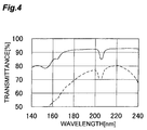
- a surface of each sample was mirror-polished with abrasive grains of diamond, and the transmittance taking account of reflection loss with respect to light having a wavelength of 140 to 240 nm was measured.
- the spectrophotometer used for measurement was VUV200 manufactured by JASCO Corporation.
- Table 1 shows the transmittance of each sample taking account of reflection loss, and its internal transmittance per 10 mm calculated from that value. Though errors were large and differences were hardly seen among the individual samples in the case of the substrate thickness at 20 mm, clear differences were recognized in the case of the substrate thickness at 30 mm such that, for example, while the internal transmittance of the sample in accordance with Example 2 was 99.7 ⁇ 0.2[%/cm], the internal transmittance in Comparative Example 1 was 99.3 ⁇ 0.2[%/cm].
- a sample having a diameter of 30 mm and a thickness of 30 mm was collected from each of the obtained calcium fluoride crystals, and its opposing two planes were optically ground with abrasive grains of diamond.
- This sample was irradiated with light emitted from an F 2 laser, and the spectral transmittance was measured before and after the light irradiation.
- the employed F 2 laser has an output of 4W and a repetition rate of 200 Hz, whereas its irradiation area is about 0.5 ⁇ 1.2 [cm 2 ], whereby the energy density per pulse (fluence) is 33 mJ/cm 2 /pulse.
- the calcium fluoride crystals of Example 1 and 2 have no absorption band at 154 nm, and its amount of decrease in transmittance with respect to light having a wavelength of 157 nm after being irradiated with 10,000 pulses of the F 2 laser was a very small value of 0.4 and 0.5[%/cm], respectively.
- their amounts of decrease were 2.0, 11.2 and 2.8[%/cm], respectively, thus exceeding the permissible value in terms of optical designing.
- the calcium fluoride crystals manufactured in Example 1 were used for making optical members constituting the illumination optical system 2 and the projection optical system 8 of Fig. 2. These optical members were used for making the projection exposure apparatus of Fig. 1 in which the illumination optical system 2 and the projection optical system 8 were constituted by only the optical members made of the calcium fluoride crystals of Example 1. Also, similarly, the projection exposure apparatus of Fig. 1 in which the illumination optical system 2 and the projection optical system 8 were constituted by only the optical members made of the calcium fluoride crystals of Example 2, the projection exposure apparatus of Fig. 1 in which the illumination optical system 2 and the projection optical system 8 were constituted by only the optical members made of the calcium fluoride crystals of Comparative Example 1, and the projection exposure apparatus of Fig. 1 in which the illumination optical system 2 and the projection optical system 8 were constituted by only the optical members made of the calcium fluoride crystals of Comparative Example 3 were manufactured.
- a photolithography apparatus having an optical system constituted by such an optical member enables finer processing when vacuum ultraviolet light such as F 2 laser light is utilized.
Landscapes
- Physics & Mathematics (AREA)
- General Physics & Mathematics (AREA)
- Crystals, And After-Treatments Of Crystals (AREA)
- Exposure And Positioning Against Photoresist Photosensitive Materials (AREA)
- Glass Compositions (AREA)
- Exposure Of Semiconductors, Excluding Electron Or Ion Beam Exposure (AREA)
Abstract
Description
wherein at least a part of optical members constituting the irradiation optical system and projection optical system is made of a calcium fluoride crystal exhibiting an internal transmittance of 99.5%/cm or greater with respect to light having a specific wavelength of 185 nm or shorter.

Claims (5)
- An optical member for photolithography comprising a calcium fluoride crystal exhibiting an internal transmittance of 99.5%/cm or greater with respect to light having a specific wavelength of 185 nm or shorter.
- An optical member according to claim 1, wherein an amount of decrease in internal transmittance when irradiated with light having an energy density of 50 mJ/cm2/pulse or less is 0.5% or less per 10 mm.
- An optical member according to claim 1, wherein said light is light emitted from an F2 laser light source.
- An optical member according to claim 1, wherein said internal transmittance is obtained by a measuring method including:a step of cutting out a measurement sample having a thickness of 30 mm or greater from an optical member made of a calcium fluoride crystal;a step of measuring a transmittance of said measurement sample at a specific wavelength of 185 nm or shorter; anda step of excluding an influence of decrease in said actually measured transmittance corresponding to a surface reflection loss, so as to calculate the internal transmittance per unit thickness.
- A photolithography apparatus comprising an exposure light source for emitting light having a wavelength of 185 nm or shorter, a mask formed with an original image of a pattern, an irradiation optical system for irradiating said mask with the light emitted from said light source, a projection optical system for projecting onto a photosensitive substrate a pattern image projected from said mask, and an alignment system for aligning said mask and said photosensitive substrate with each other;
wherein at least a part of optical members constituting said irradiation optical system and projection optical system is made of a calcium fluoride crystal exhibiting an internal transmittance of 99.5%/cm or greater with respect to light having a specific wavelength of 185 nm or shorter.
Applications Claiming Priority (4)
| Application Number | Priority Date | Filing Date | Title |
|---|---|---|---|
| JP2674699 | 1999-02-03 | ||
| JP11026746A JP2000227400A (en) | 1999-02-03 | 1999-02-03 | Optical material for optical lithography, method for measuring transmittance thereof, and optical lithography apparatus |
| JP11037481A JP2000235101A (en) | 1999-02-16 | 1999-02-16 | Ultraviolet transmission optical material and ultraviolet optical device using the same |
| JP3748199 | 1999-02-16 |
Publications (2)
| Publication Number | Publication Date |
|---|---|
| EP1026548A2 true EP1026548A2 (en) | 2000-08-09 |
| EP1026548A3 EP1026548A3 (en) | 2002-12-11 |
Family
ID=26364563
Family Applications (1)
| Application Number | Title | Priority Date | Filing Date |
|---|---|---|---|
| EP00102108A Withdrawn EP1026548A3 (en) | 1999-02-03 | 2000-02-03 | Optical member for photolithography and photolithography apparatus |
Country Status (2)
| Country | Link |
|---|---|
| US (1) | US6377332B1 (en) |
| EP (1) | EP1026548A3 (en) |
Cited By (3)
| Publication number | Priority date | Publication date | Assignee | Title |
|---|---|---|---|---|
| WO2002077676A1 (en) * | 2001-03-15 | 2002-10-03 | Nikon Corporation | Optical member and method of producing the same, and projection aligner |
| WO2004015461A1 (en) * | 2002-08-07 | 2004-02-19 | Corning Incorporated | Scatter-free uv optical fluoride crystal elements for < 200 nm laser lithography and methods |
| CN104678715A (en) * | 2003-02-26 | 2015-06-03 | 株式会社尼康 | Exposure Apparatus And Method, And Method Of Producing Apparatu |
Families Citing this family (15)
| Publication number | Priority date | Publication date | Assignee | Title |
|---|---|---|---|---|
| US6995930B2 (en) * | 1999-12-29 | 2006-02-07 | Carl Zeiss Smt Ag | Catadioptric projection objective with geometric beam splitting |
| JP2002255686A (en) * | 2001-02-26 | 2002-09-11 | Canon Inc | Calcium fluoride crystal, method and apparatus for producing the same |
| US7163649B2 (en) * | 2001-07-09 | 2007-01-16 | The United States Of America As Represented By The Secretary Of Commerce | Minimizing spatial-dispersion-induced birefringence |
| US6762738B2 (en) * | 2001-09-28 | 2004-07-13 | Brillian Corporation | Pixel circuit with shared active regions |
| WO2003052392A1 (en) * | 2001-12-13 | 2003-06-26 | Corning Incorporated | UV OPTICAL FLUORIDE CRYSTAL ELEMENTS FOR μ<200NM LASER LITHOGRAPHY AND METHODS THEREFORE |
| JP4305611B2 (en) * | 2002-07-18 | 2009-07-29 | 株式会社ニコン | Illumination optical apparatus, exposure apparatus, and exposure method |
| US20040099205A1 (en) * | 2002-09-03 | 2004-05-27 | Qiao Li | Method of growing oriented calcium fluoride single crystals |
| KR100916656B1 (en) * | 2002-10-22 | 2009-09-08 | 삼성전자주식회사 | Laser Irradiation Apparatus and Manufacturing Method of Polysilicon Thin Film Transistor Using the Same |
| US7033433B2 (en) * | 2003-01-24 | 2006-04-25 | Corning Incorporated | Crystal growth methods |
| US6863403B2 (en) * | 2003-05-27 | 2005-03-08 | Ultratech, Inc. | Deep ultraviolet unit-magnification projection optical system and projection exposure apparatus |
| US20040261690A1 (en) * | 2003-06-30 | 2004-12-30 | Ivy Malcolm N. | Method of making optical fluoride crystal feedstock |
| EP1550745A1 (en) * | 2003-12-24 | 2005-07-06 | Corning Incorporated | Metal fluoride crystals suitable for UV applications prepared from particles having a small surface area |
| US20060249072A1 (en) * | 2005-05-05 | 2006-11-09 | Csillag Frank J | Method of synthesizing a fluoride growth material for improved outgassing |
| DE102005024678B3 (en) * | 2005-05-30 | 2006-08-31 | Schott Ag | Method for specification of optical material with reduced inclination to irreversible radiation damage involving the use of laser and fluorescent energy |
| US20120057222A1 (en) * | 2010-09-03 | 2012-03-08 | Yasuhiro Hashimoto | Single crystal of magnesium fluoride, optical member and optical element comprising the same |
Family Cites Families (8)
| Publication number | Priority date | Publication date | Assignee | Title |
|---|---|---|---|---|
| US5031977A (en) * | 1989-12-27 | 1991-07-16 | General Signal Corporation | Deep ultraviolet (UV) lens for use in a photolighography system |
| JP3083952B2 (en) | 1994-04-07 | 2000-09-04 | 株式会社ニコン | Fluorite for UV optics with excellent UV resistance and method for testing transmittance of fluorite |
| JP3957782B2 (en) | 1996-03-22 | 2007-08-15 | キヤノン株式会社 | Fluorite, manufacturing method thereof and exposure apparatus |
| US6342312B2 (en) * | 1996-03-22 | 2002-01-29 | Canon Kabushiki Kaisha | Calcium fluoride crystal, optical article and exposure apparatus for photo-lithography using the same |
| JPH1059799A (en) * | 1996-08-20 | 1998-03-03 | Nikon Corp | Optical lithography equipment |
| JPH10260349A (en) * | 1997-03-18 | 1998-09-29 | Nikon Corp | Imaging optics for ultraviolet laser |
| EP0901650B1 (en) * | 1997-03-25 | 2001-09-19 | Heraeus Quarzglas GmbH & Co. KG | Optical system for integrated circuit fabrication |
| US5978070A (en) * | 1998-02-19 | 1999-11-02 | Nikon Corporation | Projection exposure apparatus |
-
2000
- 2000-01-31 US US09/494,039 patent/US6377332B1/en not_active Expired - Lifetime
- 2000-02-03 EP EP00102108A patent/EP1026548A3/en not_active Withdrawn
Cited By (6)
| Publication number | Priority date | Publication date | Assignee | Title |
|---|---|---|---|---|
| WO2002077676A1 (en) * | 2001-03-15 | 2002-10-03 | Nikon Corporation | Optical member and method of producing the same, and projection aligner |
| US6850371B2 (en) | 2001-03-15 | 2005-02-01 | Nikon Corporation | Optical member and method of producing the same, and projection aligner |
| US7166163B2 (en) | 2001-03-15 | 2007-01-23 | Nikon Corporation | Optical member, method of manufacturing the same, and projection exposure system |
| EP1369708A4 (en) * | 2001-03-15 | 2008-12-31 | Nikon Corp | Optical member and method of producing the same, and projection aligner |
| WO2004015461A1 (en) * | 2002-08-07 | 2004-02-19 | Corning Incorporated | Scatter-free uv optical fluoride crystal elements for < 200 nm laser lithography and methods |
| CN104678715A (en) * | 2003-02-26 | 2015-06-03 | 株式会社尼康 | Exposure Apparatus And Method, And Method Of Producing Apparatu |
Also Published As
| Publication number | Publication date |
|---|---|
| US6377332B1 (en) | 2002-04-23 |
| EP1026548A3 (en) | 2002-12-11 |
Similar Documents
| Publication | Publication Date | Title |
|---|---|---|
| US6377332B1 (en) | Optical member for photolithography and photolithography apparatus | |
| EP0869203B1 (en) | Calcium Fluoride crystal, optical article and production method | |
| JP4238727B2 (en) | Manufacturing method of optical member | |
| EP0720970B1 (en) | Silica glass for photolithography, optical member including the same, exposure apparatus including the same, and method for producing the same | |
| KR20030036254A (en) | Scanning exposure method and scanning exposure system, and device production method | |
| JPH10260349A (en) | Imaging optics for ultraviolet laser | |
| US6782074B2 (en) | Optical member for photolithography and method for evaluating the same | |
| KR20030082451A (en) | Optical system and method for manufacturing the same, projective optical system and method for manufacturing the same, exposure apparatus, and exposure method | |
| US6226128B1 (en) | Light-transmitting optical member, manufacturing method thereof, evaluation method therefor, and optical lithography apparatus using the optical member | |
| EP1750172A1 (en) | Wavelength converting optical system, laser light source, exposure apparatus, mask examining apparatus, and macromolecular crystal lens machining device | |
| CN101073021B (en) | Transmitting optical element and objective for a microlithographic projection exposure apparatus | |
| EP1413870A1 (en) | Optical member for optical lithography and evaluation method therefor | |
| US6727025B1 (en) | Photomask and exposure method | |
| JP3619141B2 (en) | Projection exposure apparatus and device manufacturing method | |
| US6656860B2 (en) | Synthetic silica glass member, photolithography apparatus and process for producing photolithography apparatus | |
| JPH101310A (en) | Calcium fluoride crystal, method for producing the same, and projection exposure apparatus using the same | |
| WO2001003170A1 (en) | Exposure method and device | |
| EP1050754B1 (en) | Method of measuring the transmittance of optical members for ultraviolet use | |
| US6798495B2 (en) | Exposure apparatus, exposure method and device production method | |
| EP1081106A1 (en) | Synthetic quartz glass optical member for ultraviolet light and reduction projection exposure system using the same | |
| JPH10281992A (en) | Method for measuring component concentration distribution of optical material and method for measuring light transmittance distribution | |
| JP2001002497A (en) | Optical substrate, optical element, optical system and optical lithography apparatus using the same, and optical substrate inspection method | |
| JP2000227400A (en) | Optical material for optical lithography, method for measuring transmittance thereof, and optical lithography apparatus | |
| JP2001019596A (en) | Artificial crystal for ultraviolet optics, optical substrate and optical lithography apparatus using the same | |
| JP2004157349A (en) | Optical system manufacturing method, projection optical system, exposure apparatus, and exposure method |
Legal Events
| Date | Code | Title | Description |
|---|---|---|---|
| PUAI | Public reference made under article 153(3) epc to a published international application that has entered the european phase |
Free format text: ORIGINAL CODE: 0009012 |
|
| AK | Designated contracting states |
Kind code of ref document: A2 Designated state(s): AT BE CH CY DE DK ES FI FR GB GR IE IT LI LU MC NL PT SE |
|
| AX | Request for extension of the european patent |
Free format text: AL;LT;LV;MK;RO;SI |
|
| PUAL | Search report despatched |
Free format text: ORIGINAL CODE: 0009013 |
|
| AK | Designated contracting states |
Kind code of ref document: A3 Designated state(s): AT BE CH CY DE DK ES FI FR GB GR IE IT LI LU MC NL PT SE |
|
| AX | Request for extension of the european patent |
Free format text: AL;LT;LV;MK;RO;SI |
|
| 17P | Request for examination filed |
Effective date: 20030522 |
|
| AKX | Designation fees paid |
Designated state(s): DE FR GB NL |
|
| 17Q | First examination report despatched |
Effective date: 20030723 |
|
| STAA | Information on the status of an ep patent application or granted ep patent |
Free format text: STATUS: THE APPLICATION HAS BEEN WITHDRAWN |
|
| 18W | Application withdrawn |
Effective date: 20050712 |