EP1023776B1 - Phase-locked loop and method for automatically locking to a variable input frequency - Google Patents
Phase-locked loop and method for automatically locking to a variable input frequency Download PDFInfo
- Publication number
- EP1023776B1 EP1023776B1 EP98953611A EP98953611A EP1023776B1 EP 1023776 B1 EP1023776 B1 EP 1023776B1 EP 98953611 A EP98953611 A EP 98953611A EP 98953611 A EP98953611 A EP 98953611A EP 1023776 B1 EP1023776 B1 EP 1023776B1
- Authority
- EP
- European Patent Office
- Prior art keywords
- frequency
- input signal
- division factor
- signal
- phase
- Prior art date
- Legal status (The legal status is an assumption and is not a legal conclusion. Google has not performed a legal analysis and makes no representation as to the accuracy of the status listed.)
- Expired - Lifetime
Links
- 238000000034 method Methods 0.000 title claims description 11
- 230000008859 change Effects 0.000 claims abstract description 46
- 230000001419 dependent effect Effects 0.000 claims abstract description 5
- 238000012544 monitoring process Methods 0.000 claims description 3
- 230000004044 response Effects 0.000 claims description 3
- 238000010586 diagram Methods 0.000 abstract description 17
- 230000007704 transition Effects 0.000 description 12
- 238000001514 detection method Methods 0.000 description 11
- 230000007423 decrease Effects 0.000 description 7
- 230000005540 biological transmission Effects 0.000 description 5
- 230000004048 modification Effects 0.000 description 5
- 238000012986 modification Methods 0.000 description 5
- 230000008901 benefit Effects 0.000 description 4
- 230000000694 effects Effects 0.000 description 3
- 230000003068 static effect Effects 0.000 description 3
- 230000007246 mechanism Effects 0.000 description 2
- 238000011084 recovery Methods 0.000 description 2
- 230000001052 transient effect Effects 0.000 description 2
- 206010065929 Cardiovascular insufficiency Diseases 0.000 description 1
- 239000003990 capacitor Substances 0.000 description 1
- 239000004020 conductor Substances 0.000 description 1
- 239000000284 extract Substances 0.000 description 1
- 238000012886 linear function Methods 0.000 description 1
- 230000007257 malfunction Effects 0.000 description 1
- 230000000737 periodic effect Effects 0.000 description 1
- 230000009467 reduction Effects 0.000 description 1
- 239000000758 substrate Substances 0.000 description 1
- 230000001360 synchronised effect Effects 0.000 description 1
Images


Classifications
-
- H—ELECTRICITY
- H03—ELECTRONIC CIRCUITRY
- H03L—AUTOMATIC CONTROL, STARTING, SYNCHRONISATION OR STABILISATION OF GENERATORS OF ELECTRONIC OSCILLATIONS OR PULSES
- H03L7/00—Automatic control of frequency or phase; Synchronisation
- H03L7/06—Automatic control of frequency or phase; Synchronisation using a reference signal applied to a frequency- or phase-locked loop
- H03L7/16—Indirect frequency synthesis, i.e. generating a desired one of a number of predetermined frequencies using a frequency- or phase-locked loop
- H03L7/18—Indirect frequency synthesis, i.e. generating a desired one of a number of predetermined frequencies using a frequency- or phase-locked loop using a frequency divider or counter in the loop
- H03L7/197—Indirect frequency synthesis, i.e. generating a desired one of a number of predetermined frequencies using a frequency- or phase-locked loop using a frequency divider or counter in the loop a time difference being used for locking the loop, the counter counting between numbers which are variable in time or the frequency divider dividing by a factor variable in time, e.g. for obtaining fractional frequency division
Definitions
- This invention relates to an integrated circuit and, more particularly to a phase-locked loop ("PLL”) which can, within the feedback loop of the PLL, automatically detect and incrementally or directly lock upon a change in frequency of an input signal without substantially changing the PLL output signal frequency.
- PLL phase-locked loop
- a PLL is generally used in many areas of electronics to control the frequency and/or phase of a signal. Instances of use include, for example, applications as frequency synthesizers, analog-to-digital modulators, and clock recovery circuits.
- a PLL extracts a timing reference from, for example, an incoming data stream.
- the timing reference, or recovered clock is typically synchronized to transitions of data within the data stream.
- the timing reference is output from the PLL arranged at the receiving end of, for example. a transmission channel.
- Using a PLL at the receiving end to reconstruct a clocking signal avoids having to forward with the data a separate clocking signal. It is often desirable to modify the transition rate, or frequency, of the data stream forwarded across a transmission channel.
- a PLL at the receive end of the transmission channel must be capable of accepting an input signal at a variety of frequencies. If the input signal comprises data, it is important that the PLL support both regular and high-speed data rates. If the input signal is a clocking signal, the PLL must therefore accept and be able to choose among a variety of clocking frequencies. While the input signal frequency to the PLL can vary depending on the transmission rate of the transmission mechanism (i.e.. transmitter, receiver and channel) it is generally desired that a digital circuit coupled to the PLL output run at a relatively fixed rate. In most instances. the clocking frequency of the digital circuit or digital processor must run at a frequency within the manufacturer specified frequency range.
- the output signal (hereinafter "clocking signal”) from the PLL must not exceed (or be less than) the operating specification of the digital circuit or digital processor. If the input signal frequency should change given. for example, an increase in data rate, the PLL will attempt to lock upon the changed input signal frequency. In most cases, a PLL is used in applications where the clocking signal frequency output from the PLL must be a multiple of the input signal frequency. This arises since, in most instances, the digital processor can operate at a higher frequency than the transmitted data stream.
- a clock divider is situated in the feedback loop of the PLL. The clock divider comprises a frequency division factor. An increase in the division factor will proportionally increase the clocking signal frequency relative to the input signal frequency. Thus, for example, if the input signal frequency is at 1.0x and division factor is 16. then the clocking signal frequency is 16.0x.
- a static (or fixed) division factor presents a feedback signal frequency that will be momentarily dissimilar from an increasing input signal frequency during instances of "unlock”. This will cause an increase in DC voltage to the PLL voltage controlled oscillator (“VCO"), resulting in an increase in the clocking signal frequency.
- VCO voltage controlled oscillator
- the clocking signal achieves a steady state value, and the clocking signal is divided in the PLL feedback loop to substantially match the input signal frequency, then the PLL is said to be "locked”.
- the clocking signal may exceed the maximum frequency of the digital processor to which the clocking signal is connected. If this should occur, then the digital processor may lose its internal state and/or malfunction.
- the VCO may be forced outside its dynamic operating range.
- WO97/20398 discloses a frequency synthesiser loop which includes a first voltage controlled oscillator and a first divider circuit for dividing a frequency of an outward signal generated by the first voltage controlled oscillator by a factor of M.
- the synthesiser loop further includes a phase/frequency detector circuit, a loop filter circuit, a summing circuit, a feed-forward amplifier, a second voltage controlled oscillator and a second divider circuit.
- the second divider circuit divides a second output signal generated by the second voltage controlled oscillator by a factor of M and a micro-processor varies the value of M to keep the first voltage in the middle of a range of the second voltage controlled oscillator.
- a phase-locked loop comprising a clock divider circuit arranged operably coupled to an output of a voltage controlled oscillator within a feedback loop of the phase-locked loop, said clock divider comprising a frequency division factor adapted to be modified inversely proportional to a change in frequency of an input signal forwarded to the phase-locked loop, to maintain a substantially constant output frequency of the loop, and wherein said frequency division factor is adapted to be modified by a decision circuit operably coupled to an input of the voltage controlled oscillator to determine whether the change in frequency of the input signal exceeds a threshold amount
- said frequency division factor is modified by multiplying a current frequency division factor by a positive factor M greater than 1.0., and wherein said change in frequency of said input signal is modified by multiplying a current frequency of said input signal by I/M.
- said frequency division factor is modified by multiplying a current frequency division factor by 1/M (where M is a factor greater than 1.0), and wherein said change in frequency of said input signal is modified by multiplying a current frequency of said input signal by M.
- said decision circuit comprises a plurality of comparators, each of which is connected to receive a dc voltage proportional to the change in frequency of the input signal
- each of the plurality of comparators is further connected to receive a unique reference voltage to which the dc voltage is compared.
- a phased-locked loop of the type described above is coupled to receive an input signal frequency and produce an output signal frequency, wherein a phase detector is coupled to produce a dc voltage corresponding to a difference between the input signal frequency and the output signal frequency reduced by the division factor; a voltage controlled oscillator is coupled to receive the dc voltage and change the output signal frequency dependent on the dc voltage; the clock divider circuit being coupled to receive the output frequency and, in accordance with the division factor, forward the output signal frequency reduced by the division factor to the phase detector; a decision circuit being coupled to receive the dc voltage and produce an encoded signal based on a comparison of the dc voltage to a reference voltage; and a control unit coupled to receive the encoded signal and modify the frequency division factor in response thereto.
- control unit dispatched a control signal based on a current frequency division factor and the encoded signal.
- said encoded signal comprises binary bits.
- the number of said binary bits is two.
- phase detector comprises a frequency detector.
- the invention also relates to A method for changing a clock divider within a feedback loop of a phase-locked loop for locking the frequency of an output signal to the frequency of an input signal forwarded from and to, respectively, the phase-locked loop, said method comprising monitoring a dc voltage output from a detector which compares phase and frequency of a feedback signal to the input signal, and changing the frequency of the feedback signal inversely to substantially match a change in frequency of the output signal based on a comparison of a reference voltage to the dc voltage prior the change in frequency of the input signal.
- said changing comprises reducing the frequency of the feedback signal inversely proportional to increasing the frequency of the input signal.
- said changing comprises increasing the frequency of the feedback signal inversely proportional to reducing the frequency of the input signal.
- Improvements involve, for example, inserting a decision circuit between the loop filter and VCO of the PLL.
- the decision circuit monitors DC voltage applied to the VCO indicative of a change in frequency of the input signal
- the decision circuit presents a coded signal to a control unit indicative of the DC voltage relative to one or more threshold voltages.
- the control unit responds to the coded signal by either maintaining or modifying the frequency division factor within the clock divider of the PLL feedback loop. Input to the VCO is therefore indicative of the frequency of the input signal.
- the decision circuit in combination with the control unit provide a control function that can select an appropriate division factor based on the DC voltage at the input of the VCO.
- the decision circuit can be implemented as, for example, an analog-to-digital (“A/D") converter which essentially takes a DC value and produces a digital coded signal based on the relationship of that DC value to one or more reference voltages.
- A/D analog-to-digital
- the control unit can be implemented in hardware or software to recognise various digital encoded signals in dissimilar ways and to produce a unique modification of the division factor dependent on the existing (current) division factor M or the existing division factor M and the existing (current) input signal frequency.
- the decision circuit and control unit serves to adapt the PLL via the clock divider to high speed and low speed incoming data and/or clocking input frequencies. If the input signal frequency should increase to accommodate a faster data stream, the decision circuit will respond by dispatching a coded signal based on an increase in the DC voltage at the input of the VCO, relative to a reference voltage. The coded signal will then be interpreted by the control unit based on the current status of the clock divider division factor. Depending on how the control units is programmed, an increase in the input signal frequency may preferably cause a proportional decrease in the frequency division factor of the clock divider. This will result in two important outcomes.
- the feedback signal frequency forwarded from the clock divider will substantially equate to the input signal frequency thereby locking the PLL in a rapid fashion. Without a differential between the feedback signal frequency and the input signal frequency, the DC voltage will quickly transition back to a mid-scale, locked value relative to the voltage reference values so as not to cause further transitions of the frequency division factor.
- the clocking signal output from the PLL will retain its previous frequency and will be minimally affected in the interim when the increased input signal frequency_ occurs and the time in which the frequency division factor is changed. Accordingly, the present apparatus and/or circuit achieves a rapid locked status to a variable input signal frequency without modifying or varying the clocking signal forwarded to, for example, a down-stream digital circuit,
- the feedback signal frequency may not substantially equate to a changed input signal frequency after a first iterative change of the frequency division factor.
- the DC voltage may remain or transition back above threshold even after the frequency division factor is changed.
- Another (second and subsequent) iterative change may be needed to cause the DC voltage to remain at mid-scale (i.e., to lock the input and output signal frequencies).
- the present technique can be used to determine the frequency of the changed (i.e., next) input signal or data rate.
- the decision circuit and control unit thereby allow automatic detection of the input signal frequency either directly or through iterative changes in the division factor.
- a direct change needed to rapidly lock upon the input signal implies a high resolution frequency division factor, the magnitude of differences between a current divider state and a next divider state can be any integer or fractional number.
- the present invention contemplates a PLL.
- the PLL comprises a clock divider circuit arranged within a feed back loop of the PLL.
- the clock divider comprises a frequency division factor adapted to be preferably modified inversely proportional to a change in the frequency of an input signal forwarded to the PLL.
- the frequency division factor is modified by multiplying a current frequency division factor by a positive number M greater than 1.0, and wherein the change in frequency of the input signal is modified by multiplying a current frequency of the input signal by 1/M.
- the frequency division factor can be modified by multiplying a current frequency division factor by 1/M, such that the change in frequency of the input signal is modified by multiplying a current frequency of the input signal by M.
- the present invention further contemplates an apparatus.
- the apparatus is coupled to receive an input signal frequency and produce an output signal frequency (i.e., clocking signal frequency).
- a phase detector and loop filter are coupled to produce a DC voltage corresponding to a difference between the input signal frequency and the output signal frequency reduced by a division factor.
- a VCO is coupled to receive the DC voltage and change the output signal frequency dependent on the DC voltage.
- a clock divider circuit is coupled to receive the output frequency and, in accordance with the division factor, forward the output signal frequency reduced by a division factor to the phase detector.
- a decision circuit is coupled to receive the DC voltage and produce a coded signal based on the comparison of the DC voltage to the reference voltage.
- a control unit is coupled to receive the coded signal and automatically (dynamically) modify the frequency division factor in response thereto.
- the present invention yet further contemplates a method for automatically and dynamically changing a clock divider within a feedback loop of a PLL.
- the clock divider is changed in order to directly or iteratively lock the frequency of the clocking signal to the frequency of an input signal.
- the method further includes steps of monitoring a DC voltage from a detector which compares phase and frequency of a feedback signal to the input signal.
- the frequency of the feedback signal can be changed to substantially match a change in frequency of the input signal while maintaining substantially constant the frequency of the output signal.
- the feedback signal frequency is changed based on a comparison of a reference voltage to the DC voltage prior to the readjustment of the feedback signal to bring the feedback signal frequency in line again with the changed input signal frequency.
- Fig. 1 illustrates a signal 10 input to a PLL 12.
- the input signal can be forwarded at different frequencies, shown as x, mx and x/m, wherein m represents a variation of the base frequency x. If a need exists for a higher data rate, for example, then the input signal frequency can be increased; the same applies if the data rate must be reduced.
- the frequency of the input signal is mostly a function of the transmitting and receiving component and therefore can vary dissimilar from the components within PLL 12.
- PLL 12 includes, according to one example, a phase/frequency ("PFD") detector 14, a loop filter 18, a VCO 20 and a clock divider 22.
- PFD phase/frequency
- Clock divider 22 is placed in the feedback loop of PLL 12, and provides a multiplication factor between the input signal frequency and a higher frequency output signal.
- PFD 14 can be formulated, for example, as a multiplier (or mixer) comprising an exclusive OR gate, a R-S latch or, in the instance of frequency detection, any circuit which produces non-complimentary outputs proportional to the frequency differences between the inputs.
- Loop filter 18 may be implemented with passive elements comprising a capacitor and a resistor linked between conductors bearing the output from PFD 14 and the input to VCO 20. Loop filter 18 may serve to remove transient noise from the rail-driven signal forwarded from PFD 14, and therefore provides stability to the loop.
- VCO 20 may be implemented, for example, as a ring oscillator comprising, for example, an odd number of series-connected inverters.
- the components shown in PLL 12 can be made in numerous different ways. The mechanism and circuitry needed to embody each component can vary depending on the accuracy and application desired. The examples described are therefore only examples of ways to implement each component. Variations and modifications may be made to the form and structure of each component as mandated by the application in which the components are placed.
- VCO 20 is designed to produce a periodic output whose frequency is a linear function of the DC voltage forwarded from loop filter 18. If the DC voltage increases, for example, then VCO 20 will increase the output signal frequency.
- the output signal is forwarded to the digital circuit coupled as a load to PLL 12 as well as to clock divider 22.
- Clock divider 22 includes a frequency division factor which enables the output signal (clocking signal) frequency to be a multiple of the input signal frequency.
- the clocking signal frequency is reduced (i.e., divided) before it is fed back to PFD 14.
- the frequency division factor M is modified in real-time depending on the amount of frequency multiplication needed.
- factor M is a number equal to or greater than 1.0. If M is an integer, frequency division can be suitably performed, for example, by a digital counter.
- Included with or separate from PLL 12 is a decision circuit 30 and a control unit 32.
- Decision circuit 30 is essentially a A/D converter which encodes in digital form the comparison of a reference voltage (or reference voltages) to the DC voltage forwarded to VCO 20.
- a reference voltage or reference voltages
- a first reference voltage can be configured between the mid-scale voltage and V DD
- the second reference voltage may be placed between the mid-scale voltage and ground. If, for example, the DC voltage exceeds the first reference voltage, (possibly indicating a rapid rise in the input signal frequency) the decision circuit will encode a binary signal indicating that rise.
- the input signal frequency decreases and the DC voltage extends below the second reference voltage to produce another, uniquely encoded signal. It is recognized that, however, more than two reference voltages may be used.
- Fig. 2 illustrates one example of decision circuit 30 which generally performs A/D encoding. If two reference voltages are used, then a first comparator 34 will produce a digital "1" value if the DC voltage exceeds the first reference voltage v t+ . A second comparator will produce a digital "1" value if the DC voltage is less than a second reference voltage v t- .
- the first reference voltage may be a value between mid-scale and V DD while the second reference voltage is between mid-scale and ground.
- comparators and associated reference voltages there may be numerous other comparators and associated reference voltages.
- the additional reference voltages may be spaced quantifiable distances from one another between ground and V DD to enhance resolution of the A/D converter output.
- the example shown in Fig. 2 presents a coded two-bit output.
- additional comparators and associated reference voltages can encode more than two binary bits if additional resolution of PLL frequency is desired.
- Two comparators and two reference voltages provide a two bit binary value indicative of whether the DC voltage is: (1) above v t+ , (2) between v t- and v t+ , or (3) below v t- .
- Additional comparators and reference voltages allow indication of where the DC voltage is within a closely defined voltage range.
- control unit 32 may more rapidly (and directly) respond to that voltage by transitioning to an appropriate "next" divider state knowing the current divider state. If, however, only two comparators are used, then an auto ranging function can occur. More particularly, an iterative change in divider state can occur to ultimately achieve the direct change afforded by the high resolution.
- Fig. 3 illustrates the iterative detection technique
- Fig. 4 illustrates direct detection.
- Fig. 3 is a state diagram 40 used in implementing control unit 32 according to an iterative, auto-ranging technique. Diagram 40 illustrates three states 42, 44 and 46.
- State 42 indicates a decrement in the frequency division factor within clock divider 22 if the input signal frequency, as registered by the DC voltage on decision circuit 30, is above an upper threshold (e.g., v t+ ). If the input signal frequency is not too high, then transition will occur to state 44 indicative of DC voltage between the upper and lower thresholds. Further, if the DC voltage extends below the lower threshold indicating a low frequency, then transition will occur toward state 46 from state 44. State diagram 40 presumes three detectable levels and two comparators, and the next level is adjacent the current level in magnitude. For example, if the current input frequency is 4x and the next input frequency increases to 16x, then the DC value will extend above the upper threshold and be coded as a "frequency too high" signal upon the control unit.
- an upper threshold e.g., v t+
- the control unit responds as shown by state diagram 40 by decrementing the division factor from, e.g., a ⁇ 16 to a ⁇ 15. Decrementing continues if the decision circuit again codes a frequency to high signal until eventually the proper frequency division factor is reached, e.g., ⁇ 4.
- At least one benefit in the iterative approach is its use as an input signal frequency detector. Knowing that the output signal frequency must remain relatively fixed and further knowing the current frequency division factor, one can determine the next input signal frequency when or if the input signal frequency changes. The iterative approach will change according to defined increments (i.e., integers and/or fractions) the division factor whenever the DC voltage exceeds or is less than the threshold values.
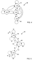
- Fig. 4 is a state diagram 48 used to implement control unit 32 according to a more direct, rapid detection/locking function. More than two levels and three comparators are required if it is necessary to change the division factor commensurate with a DC voltage within a rather narrowly defined window. In the example of Fig. 4, seven levels and eight comparators can be used to produce the various windows. Division factor can change directly between any of states 50, 52, 54 and 56. Thus, Fig. 4 indicates coding that requires at least three encoded bits (i.e., representing seven windows or states) to carry out a transition from one frequency division state to any of the others.
- Fig. 5 illustrates a more generalized state diagram of 60 used for implementing control unit 32.
- State diagram 60 can be embodied either in hardware or software to recognize a coded digital signal and therefore modify the division factor from the current frequency division factor to the next frequency division factor.
- the coded signal indicates possible change in the input signal frequency
- state diagram 60 indicates the affect of the coded signal on the clock divider 22 (shown in Fig. 1). For example, if the current division factor is modeled as x, as shown by state 62, then the division factor can change or remain in its current state. If the encoded signal is 00, then state 62 will remain.
- state 62 represents a ⁇ 4 state
- state 64 represents a ⁇ 16 state. Solely for the benefit and understanding the functionality of states 62 and 64, for the example provided, the following Table 1 is presented: CURRENT DIVIDER STATE CURRENT INPUT FREQ. COMP. HIGH COMP LOW NEXT DIVIDER STATE NEXT INPUT FREQ. CURRENT NEXT OUTPUT FREQ.
- the first line in Table 1 indicates a current divider state within clock divider 22 of a ⁇ 4. Additionally, the current input frequency is 4x (where m in Fig. 1 is equal to 4). From those pre-existing conditions, line 1 indicates the next input frequency remains at 4x. This does not produce a DC voltage which would extend above or below the threshold voltages. Accordingly, the compare high/low outputs from high comparator 34 and low comparator 36 is 00. The effect of 00 coded signal upon state 62 (where x equals 4) is no change whatsoever. Accordingly, the next divider state remains as state 62 (i.e., ⁇ 4).
- the current/next output signal frequency remains as 16x (i.e., 4x current/next input frequency times the current/next divider state).
- Table 1 indicates what would happen if the input signal frequency decreases from 4x to 1x. A decrease in DC voltage will occur as a result of the decrease in input signal frequency, thus producing a compare high/low coded signal of 01.
- the 01 coded signal as shown in Fig. 5, will cause a change in state from state 62 to state 64. This is indicated as a change in a ⁇ 4 as the current divider state to a ⁇ 16 (where m in state 64 is equal to 4).
- Lines 4 through 6 of Table 1, in conjunction with Fig. 5) indicate transition from state 64 to state 62 if the coded signal is 10. Otherwise, in the example provided, state 64 remains if the encoded signals are 00 or 01.
- Table 1 is indicative of two dissimilar input signal frequencies and two dissimilar clock divider states. Further as an example, Table 1 indicates a two-bit encoded signal derived from only two comparators and only two dissimilar threshold voltages applied to those comparators. It is recognized, however, that numerous input signal frequencies can be applied, as well as numerous clock divider states and comparators, reference voltage, etc. Regardless of the number of input signal frequencies and clock division states, the intent remains the same.
- Control unit 32 evaluates the decision circuit 30 coded output and selects the appropriate clock divider control signal value to allow PLL 12 to lock to the input signal frequency. The intent behind control unit 32 is to maintain, increase or decrease the division factor within clock divider 22 from its current value.
- the integrated circuit may include the PLL, the decision circuit and the control unit all within a single monolithic substrate. It is intended that the following claims be interpreted to embrace all such modifications and changes and, accordingly, the specification and drawings are to be regarded in an illustrative rather than a restrictive sense.
Landscapes
- Stabilization Of Oscillater, Synchronisation, Frequency Synthesizers (AREA)
- Networks Using Active Elements (AREA)
- Transmitters (AREA)
- Channel Selection Circuits, Automatic Tuning Circuits (AREA)
Abstract
Description
As a clock recovery circuit, a PLL extracts a timing reference from, for example, an incoming data stream. The timing reference, or recovered clock, is typically synchronized to transitions of data within the data stream. The timing reference is output from the PLL arranged at the receiving end of, for example. a transmission channel. Using a PLL at the receiving end to reconstruct a clocking signal avoids having to forward with the data a separate clocking signal.
It is often desirable to modify the transition rate, or frequency, of the data stream forwarded across a transmission channel. Thus, a PLL at the receive end of the transmission channel must be capable of accepting an input signal at a variety of frequencies. If the input signal comprises data, it is important that the PLL support both regular and high-speed data rates. If the input signal is a clocking signal, the PLL must therefore accept and be able to choose among a variety of clocking frequencies.
While the input signal frequency to the PLL can vary depending on the transmission rate of the transmission mechanism (i.e.. transmitter, receiver and channel) it is generally desired that a digital circuit coupled to the PLL output run at a relatively fixed rate. In most instances. the clocking frequency of the digital circuit or digital processor must run at a frequency within the manufacturer specified frequency range. Thus, when the PLL is locked upon the input signal frequency, the output signal (hereinafter "clocking signal") from the PLL must not exceed (or be less than) the operating specification of the digital circuit or digital processor. If the input signal frequency should change given. for example, an increase in data rate, the PLL will attempt to lock upon the changed input signal frequency.
In most cases, a PLL is used in applications where the clocking signal frequency output from the PLL must be a multiple of the input signal frequency. This arises since, in most instances, the digital processor can operate at a higher frequency than the transmitted data stream. To achieve a static discrepancy between the input signal and clocking signal frequencies, a clock divider is situated in the feedback loop of the PLL. The clock divider comprises a frequency division factor. An increase in the division factor will proportionally increase the clocking signal frequency relative to the input signal frequency. Thus, for example, if the input signal frequency is at 1.0x and division factor is 16. then the clocking signal frequency is 16.0x.
Broadly speaking, the present invention contemplates a PLL. The PLL comprises a clock divider circuit arranged within a feed back loop of the PLL. The clock divider comprises a frequency division factor adapted to be preferably modified inversely proportional to a change in the frequency of an input signal forwarded to the PLL. The frequency division factor is modified by multiplying a current frequency division factor by a positive number M greater than 1.0, and wherein the change in frequency of the input signal is modified by multiplying a current frequency of the input signal by 1/M. Alternatively, the frequency division factor can be modified by multiplying a current frequency division factor by 1/M, such that the change in frequency of the input signal is modified by multiplying a current frequency of the input signal by M.
The present invention further contemplates an apparatus. The apparatus is coupled to receive an input signal frequency and produce an output signal frequency (i.e., clocking signal frequency). A phase detector and loop filter are coupled to produce a DC voltage corresponding to a difference between the input signal frequency and the output signal frequency reduced by a division factor. A VCO is coupled to receive the DC voltage and change the output signal frequency dependent on the DC voltage. A clock divider circuit is coupled to receive the output frequency and, in accordance with the division factor, forward the output signal frequency reduced by a division factor to the phase detector. A decision circuit is coupled to receive the DC voltage and produce a coded signal based on the comparison of the DC voltage to the reference voltage. A control unit is coupled to receive the coded signal and automatically (dynamically) modify the frequency division factor in response thereto.
The present invention yet further contemplates a method for automatically and dynamically changing a clock divider within a feedback loop of a PLL. The clock divider is changed in order to directly or iteratively lock the frequency of the clocking signal to the frequency of an input signal. The method further includes steps of monitoring a DC voltage from a detector which compares phase and frequency of a feedback signal to the input signal. The frequency of the feedback signal can be changed to substantially match a change in frequency of the input signal while maintaining substantially constant the frequency of the output signal. The feedback signal frequency is changed based on a comparison of a reference voltage to the DC voltage prior to the readjustment of the feedback signal to bring the feedback signal frequency in line again with the changed input signal frequency.
The components shown in
Included with or separate from
Fig. 2 illustrates one example of
Two comparators and two reference voltages provide a two bit binary value indicative of whether the DC voltage is: (1) above vt+, (2) between vt- and vt+, or (3) below vt-. Additional comparators and reference voltages allow indication of where the DC voltage is within a closely defined voltage range. Given close indication of DC voltage,
Fig. 3 is a state diagram 40 used in implementing
At least one benefit in the iterative approach is its use as an input signal frequency detector. Knowing that the output signal frequency must remain relatively fixed and further knowing the current frequency division factor, one can determine the next input signal frequency when or if the input signal frequency changes. The iterative approach will change according to defined increments (i.e., integers and/or fractions) the division factor whenever the DC voltage exceeds or is less than the threshold values. Those increments will eventually cause the DC voltage to remain near
Fig. 4 is a state diagram 48 used to implement
For example, if the current division factor is modeled as x, as shown by
An examination of state diagram 60 indicates an increase in the frequency division factor from
To aid in understanding how state diagram 60 might be carried out according to one example, a further example will be presented. Assuming x within
| CURRENT DIVIDER STATE | CURRENT INPUT FREQ. | COMP. HIGH | COMP LOW | NEXT DIVIDER STATE | NEXT INPUT FREQ. | CURRENT NEXT OUTPUT FREQ. |
| ÷ 4 | 4x | 0 | 0 | ÷ 4 | 4x | 16x |
| ÷ 4 | 4x | 0 | 1 | ÷ 16 | 1 x | 16x |
| ÷ 4 | 4x | 1 | 0 | ÷ 4 | 4x | 16x |
| ÷ 16 | 1 x | 0 | 0 | ÷ 16 | 1 x | 16 x |
| ÷ 16 | 1 x | 0 | 1 | ÷ 16 | 1 x | 16x |
| ÷ 16 | 1 x | 1 | 0 | ÷ 4 | 4 x | 16x |
The next line of Table 1 indicates what would happen if the input signal frequency decreases from 4x to 1x. A decrease in DC voltage will occur as a result of the decrease in input signal frequency, thus producing a compare high/low coded signal of 01. The 01 coded signal, as shown in Fig. 5, will cause a change in state from
Line 3 in Table 1 becomes apparent given the previous descriptions of lines 1 and 2. However, it is illustrated that, as an example, a compare high/low encoded signal of 10 may not effect (or change) the divide-by-state. However, it is understood that, if desired, a 10 encoded value may cause a state transition if there are more than two states. In the example of Table 1, only two states are illustrated only for sake of brevity. Fig. 5, however, depicts a third state, and possibly numerous other states, and the effect of coded
Lines 4 through 6 of Table 1, in conjunction with Fig. 5) indicate transition from
The example shown in Table 1 is indicative of two dissimilar input signal frequencies and two dissimilar clock divider states. Further as an example, Table 1 indicates a two-bit encoded signal derived from only two comparators and only two dissimilar threshold voltages applied to those comparators. It is recognized, however, that numerous input signal frequencies can be applied, as well as numerous clock divider states and comparators, reference voltage, etc. Regardless of the number of input signal frequencies and clock division states, the intent remains the same. If the input signal frequency is higher than the feedback signal frequency forwarded from the clock divider, the feedback loop will cause the VCO input voltage to increase to try and match the input signal frequency. Similarly, if the input signal frequency is below the feed back signal frequency , the feedback loop will cause the VCO input voltage to decrease and try and match the input signal frequency. If any of the comparators produce a "1" output, this means the input signal frequency is either too high or too low for the current frequency range set by
The intent behind
It will be appreciated by those skilled in the art having the benefit of this disclosure that this invention is believed to be capable of applications with any integrated circuit having both analog and digital portions. The integrated circuit may include the PLL, the decision circuit and the control unit all within a single monolithic substrate. It is intended that the following claims be interpreted to embrace all such modifications and changes and, accordingly, the specification and drawings are to be regarded in an illustrative rather than a restrictive sense.
Claims (13)
- A phase-locked loop (12), comprising a clock divider circuit (22) arranged operably coupled to an output of a voltage controlled oscillator (20) within a feedback loop of the phase-locked loop (12), characterised in that said clock divider comprises a frequency division factor adapted to be modified inversely proportional to a change in frequency of an input signal forwarded to the phase-locked loop, to maintain a substantially constant output frequency of the loop, and wherein said frequency division factor is adapted to be modified by a decision circuit (30) operably coupled to an input of the voltage controlled oscillator to determine whether the change in frequency of the input signal exceeds a threshold amount.
- The phase-locked loop as recited in Claim 1, wherein said frequency division factor is modified by multiplying a current frequency division factor by a positive factor M greater than 1.0., and wherein said change in frequency of said input signal is modified by multiplying a current frequency of said input signal by I/M.
- The phase-locked loop as recited in Claim 1, wherein said frequency division factor is modified by multiplying a current frequency division factor by 1/M (where M is a factor greater than 1.0), and wherein said change in frequency of said input signal is modified by multiplying a current frequency of said input signal by M.
- The phase-locked loop as recited in any one of the preceding Claims wherein said decision circuit (20) comprises a plurality of comparators (34, 36), each of which is connected to receive a dc voltage proportional to the change in frequency of the input signal.
- The phase-locked loop as recited in Claim 4, wherein each of the plurality of comparators (34) is further connected to receive a unique reference voltage to which the dc voltage is compared.
- A phase-locked loop according to Claim 1 coupled to receive an input signal frequency and produce an output signal frequency, wherein a phase detector (14) is coupled to produce a dc voltage corresponding to a difference between the input signal frequency and the output signal frequency reduced by the division factor; a voltage controlled oscillator (20) is coupled to receive the dc voltage and change the output signal frequency dependent on the dc voltage; the clock divider circuit (22) being coupled to receive the output frequency and, in accordance with the division factor, forward the output signal frequency reduced by the division factor to the phase detector (14), a decision circuit (30) being coupled to receive the dc voltage and produce an encoded signal based on a comparison of the dc voltage to a reference voltage; and a control unit (32) coupled to receive the encoded signal and modify the frequency division factor in response thereto.
- The phase-locked loop as recited in Claim 6, wherein said control unit (32) dispatched a control signal based on a current frequency division factor and the encoded signal.
- The phase-locked loop recited in Claim 6 or 7, wherein said encoded signal comprises binary bits.
- The phase-locked loop as recited in Claim 8, wherein the number of said binary bits is two.
- The phase-locked loop as recited in any one of Claims 6 to 9, wherein said phase detector (14) comprises a frequency detector.
- A method for changing a clock divider within a feedback loop of a phase-locked loop for locking the frequency of an output signal to the frequency of an input signal forwarded from and to, respectively, the phase-locked loop, characterised in that said method comprises monitoring a dc voltage output from a detector which compares phase and frequency of a feedback signal to the input signal, and changing the frequency of the feedback signal inversely to substantially match a change in frequency of the output signal based on a comparison of a reference voltage to the dc voltage prior the change in frequency of the input signal.
- The method as recited in Claim 11, wherein said changing comprises reducing the frequency of the feedback signal inversely proportional to increasing the frequency of the input signal.
- The method as recited in Claim 11, wherein said changing comprises increasing the frequency of the feedback signal inversely proportional to reducing the frequency of the input signal.
Applications Claiming Priority (3)
| Application Number | Priority Date | Filing Date | Title |
|---|---|---|---|
| US951650 | 1997-10-16 | ||
| US08/951,650 US6049254A (en) | 1997-10-16 | 1997-10-16 | Phase-locked loop which can automatically adjust to and lock upon a variable input frequency |
| PCT/US1998/021889 WO1999019987A1 (en) | 1997-10-16 | 1998-10-16 | Phase-locked loop and method for automatically locking to a variable input frequency |
Publications (2)
| Publication Number | Publication Date |
|---|---|
| EP1023776A1 EP1023776A1 (en) | 2000-08-02 |
| EP1023776B1 true EP1023776B1 (en) | 2003-02-12 |
Family
ID=25491969
Family Applications (1)
| Application Number | Title | Priority Date | Filing Date |
|---|---|---|---|
| EP98953611A Expired - Lifetime EP1023776B1 (en) | 1997-10-16 | 1998-10-16 | Phase-locked loop and method for automatically locking to a variable input frequency |
Country Status (7)
| Country | Link |
|---|---|
| US (1) | US6049254A (en) |
| EP (1) | EP1023776B1 (en) |
| JP (1) | JP2001520471A (en) |
| AT (1) | ATE232663T1 (en) |
| AU (1) | AU1094199A (en) |
| DE (1) | DE69811384T2 (en) |
| WO (1) | WO1999019987A1 (en) |
Families Citing this family (17)
| Publication number | Priority date | Publication date | Assignee | Title |
|---|---|---|---|---|
| KR100360995B1 (en) * | 2000-03-03 | 2002-11-23 | 닛본 덴기 가부시끼가이샤 | Phase locked loop circuit and frequency m0dulation method in the same |
| US6664775B1 (en) * | 2000-08-21 | 2003-12-16 | Intel Corporation | Apparatus having adjustable operational modes and method therefore |
| JP4546716B2 (en) * | 2003-11-10 | 2010-09-15 | シャープ株式会社 | PLL clock signal generation circuit |
| KR100652390B1 (en) * | 2004-12-11 | 2006-12-01 | 삼성전자주식회사 | Phase locked loop circuit having a deadlock prevention circuit and a deadlock prevention method thereof |
| US7158443B2 (en) * | 2005-06-01 | 2007-01-02 | Micron Technology, Inc. | Delay-lock loop and method adapting itself to operate over a wide frequency range |
| JP2007129306A (en) | 2005-11-01 | 2007-05-24 | Nec Corp | PLL control circuit |
| KR100849222B1 (en) * | 2006-04-10 | 2008-07-31 | 삼성전자주식회사 | Transmission frequency control method used in serial transmission method, recording medium and apparatus recording the same |
| US7602253B2 (en) * | 2006-12-11 | 2009-10-13 | Silicon Image, Inc. | Adaptive bandwidth phase locked loop with feedforward divider |
| US8831140B2 (en) * | 2007-03-16 | 2014-09-09 | Altera Corporation | Protocol-agnostic automatic rate negotiation for high-speed serial interface in a programmable logic device |
| CN101572543A (en) * | 2008-05-04 | 2009-11-04 | 华为技术有限公司 | Method and device for stabilizing clock |
| JP2010062707A (en) | 2008-09-02 | 2010-03-18 | Nec Electronics Corp | Phase locked loop circuit |
| JP2010135956A (en) * | 2008-12-03 | 2010-06-17 | Renesas Electronics Corp | PLL circuit and control method thereof |
| US8477831B2 (en) | 2010-02-17 | 2013-07-02 | Altera Corporation | Multi-protocol multiple-data-rate auto-speed negotiation architecture for a device |
| CN102098044A (en) * | 2010-12-10 | 2011-06-15 | 青岛海信信芯科技有限公司 | Pixel phase lock clock frequency generating method and device |
| US8188766B1 (en) | 2011-02-10 | 2012-05-29 | Avago Technologies Enterprise IP (Singapore) Pte. Ltd. | Self-contained systems including scalable and programmable divider architectures and methods for generating a frequency adjustable clock signal |
| US8598925B1 (en) | 2012-07-16 | 2013-12-03 | Nanowave Technologies Inc. | Frequency determination circuit and method |
| DE102018121971A1 (en) | 2018-09-10 | 2020-03-12 | Gustav Klauke Gmbh | Press tool |
Family Cites Families (7)
| Publication number | Priority date | Publication date | Assignee | Title |
|---|---|---|---|---|
| JPS5354456A (en) * | 1976-10-27 | 1978-05-17 | Mitsubishi Electric Corp | Phase synchronizing oscillator |
| US4516083A (en) * | 1982-05-14 | 1985-05-07 | Motorola, Inc. | Fast lock PLL having out of lock detector control of loop filter and divider |
| DE3803965C2 (en) * | 1988-02-10 | 1993-11-25 | Bosch Gmbh Robert | Circuit arrangement with a voltage controlled oscillator |
| US5281926A (en) * | 1992-10-06 | 1994-01-25 | Zenith Electronics Corp. | Phase locked loop made operative when stable input sync signal is detected |
| US5371480A (en) * | 1992-12-04 | 1994-12-06 | Telefonaktiebolaget L M Ericsson | Step controlled signal generator |
| US5334952A (en) * | 1993-03-29 | 1994-08-02 | Spectralink Corporation | Fast settling phase locked loop |
| US5737694A (en) * | 1995-11-30 | 1998-04-07 | Scientific-Atlanta, Inc. | Highly stable frequency synthesizer loop with feedforward |
-
1997
- 1997-10-16 US US08/951,650 patent/US6049254A/en not_active Expired - Lifetime
-
1998
- 1998-10-16 AU AU10941/99A patent/AU1094199A/en not_active Abandoned
- 1998-10-16 AT AT98953611T patent/ATE232663T1/en not_active IP Right Cessation
- 1998-10-16 EP EP98953611A patent/EP1023776B1/en not_active Expired - Lifetime
- 1998-10-16 JP JP2000516436A patent/JP2001520471A/en active Pending
- 1998-10-16 WO PCT/US1998/021889 patent/WO1999019987A1/en not_active Ceased
- 1998-10-16 DE DE69811384T patent/DE69811384T2/en not_active Expired - Lifetime
Also Published As
| Publication number | Publication date |
|---|---|
| DE69811384D1 (en) | 2003-03-20 |
| DE69811384T2 (en) | 2003-12-11 |
| WO1999019987A1 (en) | 1999-04-22 |
| JP2001520471A (en) | 2001-10-30 |
| AU1094199A (en) | 1999-05-03 |
| US6049254A (en) | 2000-04-11 |
| EP1023776A1 (en) | 2000-08-02 |
| ATE232663T1 (en) | 2003-02-15 |
Similar Documents
| Publication | Publication Date | Title |
|---|---|---|
| US6049254A (en) | Phase-locked loop which can automatically adjust to and lock upon a variable input frequency | |
| US6133797A (en) | Self calibrating VCO correction circuit and method of operation | |
| US5168245A (en) | Monolithic digital phaselock loop circuit having an expanded pull-in range | |
| US5870002A (en) | Phase-frequency lock detector | |
| US6927611B2 (en) | Semidigital delay-locked loop using an analog-based finite state machine | |
| EP0866559B1 (en) | Phase-locked loop | |
| US6150889A (en) | Circuit and method for minimizing recovery time | |
| US6760389B1 (en) | Data recovery for non-uniformly spaced edges | |
| US6111468A (en) | Charge pump with charge/discharge amount control | |
| US7184512B2 (en) | Phase locked loop circuit and optical communications receiving apparatus | |
| US6915081B2 (en) | PLL circuit and optical communication reception apparatus | |
| WO1990015482A1 (en) | Dual state phase detector having frequency steering capability | |
| EP2136472A1 (en) | Fast-locking bang-bang PLL with low output jitter | |
| US20040036087A1 (en) | Semiconductor integrated circuit | |
| US20080191760A1 (en) | PLLS covering wide operating frequency ranges | |
| US6940323B2 (en) | Phase locked loop circuit with an unlock detection circuit and a switch | |
| US7145398B2 (en) | Coarse frequency detector system and method thereof | |
| US6362693B2 (en) | Frequency detection method for adjusting a clock signal frequency and a frequency detector circuit for carrying out the method | |
| US7279992B2 (en) | Circuit for detecting phase errors and generating control signals and PLL using the same | |
| US7317778B2 (en) | Phase-locked loop control circuit | |
| US5293445A (en) | AGC with non-linear gain for PLL circuits | |
| US6545546B2 (en) | PLL circuit and optical communication reception apparatus | |
| US6577695B1 (en) | Emulating narrow band phase-locked loop behavior on a wide band phase-locked loop | |
| US7123065B1 (en) | Method of improving lock acquisition times in systems with a narrow frequency range | |
| US11038513B1 (en) | Phase-locked loop with reduced frequency transients |
Legal Events
| Date | Code | Title | Description |
|---|---|---|---|
| PUAI | Public reference made under article 153(3) epc to a published international application that has entered the european phase |
Free format text: ORIGINAL CODE: 0009012 |
|
| 17P | Request for examination filed |
Effective date: 20000414 |
|
| AK | Designated contracting states |
Kind code of ref document: A1 Designated state(s): AT DE FI FR GB IT NL SE |
|
| GRAH | Despatch of communication of intention to grant a patent |
Free format text: ORIGINAL CODE: EPIDOS IGRA |
|
| GRAH | Despatch of communication of intention to grant a patent |
Free format text: ORIGINAL CODE: EPIDOS IGRA |
|
| GRAA | (expected) grant |
Free format text: ORIGINAL CODE: 0009210 |
|
| AK | Designated contracting states |
Designated state(s): AT DE FI FR GB IT NL SE |
|
| REG | Reference to a national code |
Ref country code: GB Ref legal event code: FG4D |
|
| REF | Corresponds to: |
Ref document number: 69811384 Country of ref document: DE Date of ref document: 20030320 Kind code of ref document: P |
|
| REG | Reference to a national code |
Ref country code: SE Ref legal event code: TRGR |
|
| RAP2 | Party data changed (patent owner data changed or rights of a patent transferred) |
Owner name: OASIS SILICON SYSTEMS INC. |
|
| NLT1 | Nl: modifications of names registered in virtue of documents presented to the patent office pursuant to art. 16 a, paragraph 1 |
Owner name: OASIS SILICON SYSTEMS, INC. |
|
| NLT2 | Nl: modifications (of names), taken from the european patent patent bulletin |
Owner name: OASIS SILICON SYSTEMS INC. |
|
| ET | Fr: translation filed | ||
| PLBE | No opposition filed within time limit |
Free format text: ORIGINAL CODE: 0009261 |
|
| STAA | Information on the status of an ep patent application or granted ep patent |
Free format text: STATUS: NO OPPOSITION FILED WITHIN TIME LIMIT |
|
| 26N | No opposition filed |
Effective date: 20031113 |
|
| REG | Reference to a national code |
Ref country code: FR Ref legal event code: CD Ref country code: FR Ref legal event code: CA |
|
| REG | Reference to a national code |
Ref country code: GB Ref legal event code: 732E |
|
| REG | Reference to a national code |
Ref country code: FR Ref legal event code: TP |
|
| PGFP | Annual fee paid to national office [announced via postgrant information from national office to epo] |
Ref country code: AT Payment date: 20071026 Year of fee payment: 10 |
|
| PGFP | Annual fee paid to national office [announced via postgrant information from national office to epo] |
Ref country code: NL Payment date: 20081005 Year of fee payment: 11 |
|
| PGFP | Annual fee paid to national office [announced via postgrant information from national office to epo] |
Ref country code: FI Payment date: 20081014 Year of fee payment: 11 |
|
| PG25 | Lapsed in a contracting state [announced via postgrant information from national office to epo] |
Ref country code: AT Free format text: LAPSE BECAUSE OF NON-PAYMENT OF DUE FEES Effective date: 20081016 |
|
| PGFP | Annual fee paid to national office [announced via postgrant information from national office to epo] |
Ref country code: IT Payment date: 20091015 Year of fee payment: 12 |
|
| REG | Reference to a national code |
Ref country code: NL Ref legal event code: V1 Effective date: 20100501 |
|
| PG25 | Lapsed in a contracting state [announced via postgrant information from national office to epo] |
Ref country code: NL Free format text: LAPSE BECAUSE OF NON-PAYMENT OF DUE FEES Effective date: 20100501 |
|
| PG25 | Lapsed in a contracting state [announced via postgrant information from national office to epo] |
Ref country code: FI Free format text: LAPSE BECAUSE OF NON-PAYMENT OF DUE FEES Effective date: 20091016 |
|
| PGFP | Annual fee paid to national office [announced via postgrant information from national office to epo] |
Ref country code: FR Payment date: 20101109 Year of fee payment: 13 |
|
| PG25 | Lapsed in a contracting state [announced via postgrant information from national office to epo] |
Ref country code: IT Free format text: LAPSE BECAUSE OF NON-PAYMENT OF DUE FEES Effective date: 20101016 |
|
| REG | Reference to a national code |
Ref country code: FR Ref legal event code: ST Effective date: 20120629 |
|
| PG25 | Lapsed in a contracting state [announced via postgrant information from national office to epo] |
Ref country code: FR Free format text: LAPSE BECAUSE OF NON-PAYMENT OF DUE FEES Effective date: 20111102 |
|
| PGFP | Annual fee paid to national office [announced via postgrant information from national office to epo] |
Ref country code: GB Payment date: 20170925 Year of fee payment: 20 |
|
| PGFP | Annual fee paid to national office [announced via postgrant information from national office to epo] |
Ref country code: SE Payment date: 20170925 Year of fee payment: 20 |
|
| PGFP | Annual fee paid to national office [announced via postgrant information from national office to epo] |
Ref country code: DE Payment date: 20170920 Year of fee payment: 20 |
|
| REG | Reference to a national code |
Ref country code: DE Ref legal event code: R071 Ref document number: 69811384 Country of ref document: DE |
|
| REG | Reference to a national code |
Ref country code: GB Ref legal event code: PE20 Expiry date: 20181015 |
|
| REG | Reference to a national code |
Ref country code: SE Ref legal event code: EUG |
|
| PG25 | Lapsed in a contracting state [announced via postgrant information from national office to epo] |
Ref country code: GB Free format text: LAPSE BECAUSE OF EXPIRATION OF PROTECTION Effective date: 20181015 |