EP1023638B1 - Apparatus for a laser writer for complex microlithographic patterns with a delay circuit - Google Patents
Apparatus for a laser writer for complex microlithographic patterns with a delay circuit Download PDFInfo
- Publication number
- EP1023638B1 EP1023638B1 EP98950562A EP98950562A EP1023638B1 EP 1023638 B1 EP1023638 B1 EP 1023638B1 EP 98950562 A EP98950562 A EP 98950562A EP 98950562 A EP98950562 A EP 98950562A EP 1023638 B1 EP1023638 B1 EP 1023638B1
- Authority
- EP
- European Patent Office
- Prior art keywords
- delay
- clock
- time
- signal
- delay circuit
- Prior art date
- Legal status (The legal status is an assumption and is not a legal conclusion. Google has not performed a legal analysis and makes no representation as to the accuracy of the status listed.)
- Expired - Lifetime
Links
- 238000000034 method Methods 0.000 claims abstract description 21
- 230000001934 delay Effects 0.000 claims abstract description 8
- 230000003111 delayed effect Effects 0.000 claims description 6
- 238000012545 processing Methods 0.000 claims description 4
- 230000001360 synchronised effect Effects 0.000 claims description 4
- 238000005516 engineering process Methods 0.000 claims description 3
- 239000004065 semiconductor Substances 0.000 claims description 3
- 230000007704 transition Effects 0.000 claims description 2
- 230000000295 complement effect Effects 0.000 claims 1
- 229910044991 metal oxide Inorganic materials 0.000 claims 1
- 150000004706 metal oxides Chemical class 0.000 claims 1
- 238000004377 microelectronic Methods 0.000 abstract description 3
- 230000003287 optical effect Effects 0.000 abstract description 2
- 238000001259 photo etching Methods 0.000 abstract description 2
- 238000011161 development Methods 0.000 description 3
- 230000007246 mechanism Effects 0.000 description 3
- 239000000758 substrate Substances 0.000 description 3
- 239000003990 capacitor Substances 0.000 description 2
- 230000014509 gene expression Effects 0.000 description 2
- 238000012806 monitoring device Methods 0.000 description 2
- 230000035945 sensitivity Effects 0.000 description 2
- 230000008859 change Effects 0.000 description 1
- 230000001419 dependent effect Effects 0.000 description 1
- 230000006866 deterioration Effects 0.000 description 1
- 230000003292 diminished effect Effects 0.000 description 1
- 230000003467 diminishing effect Effects 0.000 description 1
- 230000000694 effects Effects 0.000 description 1
- 230000006870 function Effects 0.000 description 1
- 238000009434 installation Methods 0.000 description 1
- 238000005259 measurement Methods 0.000 description 1
- 230000015654 memory Effects 0.000 description 1
- 238000001393 microlithography Methods 0.000 description 1
- 238000012544 monitoring process Methods 0.000 description 1
- 230000005658 nuclear physics Effects 0.000 description 1
Images

Classifications
-
- G—PHYSICS
- G03—PHOTOGRAPHY; CINEMATOGRAPHY; ANALOGOUS TECHNIQUES USING WAVES OTHER THAN OPTICAL WAVES; ELECTROGRAPHY; HOLOGRAPHY
- G03F—PHOTOMECHANICAL PRODUCTION OF TEXTURED OR PATTERNED SURFACES, e.g. FOR PRINTING, FOR PROCESSING OF SEMICONDUCTOR DEVICES; MATERIALS THEREFOR; ORIGINALS THEREFOR; APPARATUS SPECIALLY ADAPTED THEREFOR
- G03F7/00—Photomechanical, e.g. photolithographic, production of textured or patterned surfaces, e.g. printing surfaces; Materials therefor, e.g. comprising photoresists; Apparatus specially adapted therefor
- G03F7/70—Microphotolithographic exposure; Apparatus therefor
- G03F7/70383—Direct write, i.e. pattern is written directly without the use of a mask by one or multiple beams
- G03F7/704—Scanned exposure beam, e.g. raster-, rotary- and vector scanning
-
- H—ELECTRICITY
- H04—ELECTRIC COMMUNICATION TECHNIQUE
- H04N—PICTORIAL COMMUNICATION, e.g. TELEVISION
- H04N1/00—Scanning, transmission or reproduction of documents or the like, e.g. facsimile transmission; Details thereof
- H04N1/04—Scanning arrangements, i.e. arrangements for the displacement of active reading or reproducing elements relative to the original or reproducing medium, or vice versa
- H04N1/047—Detection, control or error compensation of scanning velocity or position
-
- H—ELECTRICITY
- H04—ELECTRIC COMMUNICATION TECHNIQUE
- H04N—PICTORIAL COMMUNICATION, e.g. TELEVISION
- H04N2201/00—Indexing scheme relating to scanning, transmission or reproduction of documents or the like, and to details thereof
- H04N2201/04—Scanning arrangements
- H04N2201/047—Detection, control or error compensation of scanning velocity or position
- H04N2201/04753—Control or error compensation of scanning position or velocity
- H04N2201/04758—Control or error compensation of scanning position or velocity by controlling the position of the scanned image area
- H04N2201/04767—Control or error compensation of scanning position or velocity by controlling the position of the scanned image area by controlling the timing of the signals, e.g. by controlling the frequency o phase of the pixel clock
- H04N2201/04781—Controlling the phase of the signals
- H04N2201/04784—Controlling the phase of the signals using one or more clock signals selected from a number of clock signals of different phases
Definitions
- the invention relates to a method and an apparatus for producing microlithography, in particular to the writing of photomasks for and direct writing of computer displays, microelectronic devices, and precision photo-etching, with the use of a time delay circuit such as is known from European Patent EP 0 467 076, for example. It is also applicable to optical devices and a variety of electronic interconnection structures such as multichip modules. Other applications are possible, such as printing and graphics, as well as laser projection displays.
- the writing system for semiconductor masks must be capable of writing features specified in units of 10 nm (nanometers) or less. It has been disclosed in European Patent EP 0 467 076 by the same applicant that a combination of time delays and analog power modulation can be used to achieve an arbitrarily small address grid. The same patent also discloses the use of several beams and parallel data paths to increase the through-put of the writing system.
- the present invention relates to a method and apparatus for writing of lithographic patterns with raster scanning technique comprising the use of an electronic clock to control the modulation of the beam where the placement in the scanning directions of pattern elements is controlled by time delays of at least one clock signal by fractions of a clock period.
- the invention is characterised in that said clock period is divided into a number of equally spaced time values by means of a delay-locked loop and a particular time value is chosen according to a digital control word.
- the delay circuit comprises N delay elements, each providing an additional delay of 1/N of the clock period, whereby N is digitally adjustable between at least two predetermined values, preferably 50, 60 and 64.
- N is digitally adjustable between at least two predetermined values, preferably 50, 60 and 64.
- the clock period can be exactly divided by several different numbers, diminishing the problem with rounding errors.
- any time period can be digitally represented by a binary word for the number of complete clock periods and a binary word for the additional delay as a number of 1/N fractions of a clock period.
- any period of time becomes very easy to state and communicate.
- the delay circuit is used for providing an address resolution significantly higher than what is given by the electronic clock, by time delay in the respective clock periods.
- the delay circuit is used to delay the input clock signal of the electronic clock for certain logic components, such as components for adjusting the beam relative to other beams in the case of multiple beam writing, or components for fine adjustment of the placement of the whole pattern in the scanning direction.
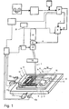
- Fig. 1 showing an apparatus according to the prior art for producing surface patterns or structures on photosensitively coated supports or substrates.
- the substrate 3 is disposed on an object table 19 which is movable in the X- and Y-directions.
- a writing head with a focusing lens 15 and a deflector device 14 is arranged to be stationary in the X- and Y-directions.
- a laser beam source 13 produces a laser beam which is modulated in regard to its power and in particular its intensity by a modulator device 5.
- the focusing lens 15 focuses on the laser beam and forms a focused laser beam as indicated at 1, which is directed on to the surface of the substrate 3.
- the apparatus For monitoring the positioning of the object table 19, the apparatus has position monitoring devices 18x and 18y which monitor the positioning of the object table 19 in the X- and Y-directions relative to the writing head (deflector device 14 and focusing lens 15). Together with electric motors 17x and 17y, the position monitoring devices 18x and 18y form a servo mechanism which produces the precisely controlled movement of the object table 19.
- the servo mechanism produces stripes 30 of a given width when the laser beam 1 scans along the scan lines 2 in the X-direction at a constant speed.
- the X-servo mechanism performs a retrace stroke movement into the starting position and the object table 19 is then moved in the Y-direction by the width of a stripe by the electric motor 17y.
- the laser beam from the source 13 is passed through the acousto-optical modulator 5 which is actuated by a high-frequency modulation drive signal 4.
- the modulation drive signal 4 is supplied by the modulator driver logic means 6.
- the intensity or power of the modulation drive signal 4 is controlled by an analog modulation drive signal of a digital-analog converter.
- the digital-analog converter which is disposed in the modulator driver stage or logic means 6, as shown in Fig. 3, is controlled by a power control signal 7 by way of a storage device which is preferably in the form of a register, for storage of the digital power control word required for producing the control effect.
- the data delivery means includes a clock having a predetermined clock period between clock pulses, so as to establish a regular train of clock pulses.
- a data processing unit is provided for accepting input data and computing or establishing beam intensity data and beam position data for an edge in the pattern to be written. Both the beam intensity data and the beam position data are established in a digital format.
- the apparatus also includes as part of the data delivery means a signal processing unit for converting the beam position data to an equivalent time for positioning the laser beam along the scan line during scanning. Particularly, this equivalent time is converted as an integer number of clock pulses plus a fractional remainder.
- digital counting means may be provided for generating a timing pulse at a time corresponding to the integer number of clock pulses and a time delay circuit may be provided for incurring to the timing pulse a time delay equal to the fractional remainder.
- a circuit may be used for setting the modulator input signal to the digital beam intensity data at the arrival of the timing pulse.
- Fig. 2 showing a preferred embodiment of the modulator drive logic means 6 described above with reference to Fig. 1. It has two storage devices for bit words, in the form of registers 605 and 608.
- the register 605 is loaded with intensity or power data 7 coming from the data delivery device 24 shown in Fig. 1.
- the register 608 is loaded with position or delay data 25 which also come from the data delivery device 24. That takes place on the basis of a transition caused by the clock signal 31.
- a digital-analog converter 606 is also operated by power data previously stored in the storage device 607. It may also be in the form of a register.
- a digitally controlled delay circuit 609 transfers the clock signal 31 to its output side, with a delay which depends on the data stored in the register 608.
- the active edge of the clock signal is supplied at the output 610 of the delay circuit 609.
- the value stored in the register 605 is loaded into the register 607 and passed to the input side of the digital-analog converter 606.
- a fresh analog power control signal 4 occurs at the output of the modulator driver stage of the modulator device 5 (fig. 1).
- the delay circuits were digitally controlled analog delay circuits.
- These analog delay circuits have several drawbacks. For example the minimum time step is comparatively large, there is a strong need for individual adjustments to the clock, the latency period is significantly large, whereby there is a need for several delay circuits working by turns, there is a large sensitivity for external disturbances and the speed is very limited.
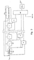
- the delay circuit comprises a delayed-locked-loop, which in turn comprises N serially connected delay elements 301, where N is an integer larger than two.
- Each delay elements delays a reference signal from the clock, with a quantum of time. This quantum of time is preferably the same for all the elements, i.e. 1/N of a clock period.
- the delay circuit can also comprise several delayed-locked loops.
- the circuit also comprises a phase comparator 302 connected to the output of the last delay element for receiving the routed delayed signal and the reference signal from the clock. Thereby the phase comparator 302 generates a control signal indicative of a difference between a phase of said routed delay signal and a phase of said reference signal.
- the output of the phase comparator is connected to said delay elements for transferring the control signal to the delay elements whereby each of the delay elements adjusts such that the phase of said reference signal is synchronized with the phase of said routed delay signal. That is, the delay circuit comprises a feedback system which automatically adjusts the amount of delay in each delay step.
- Circuits using the delayed-locked-loop technique is known from e.g. US patent 4 338 569. These known circuits have been used in completely different areas, though: adjustment of clock skew and time measurements (mainly in the area of nuclear physics and the like).
- the delay circuit of the invention also comprises a selecting part, preferably comprising a multiplexer 303 being connected to the delay elements for receiving the delayed signals generated by the delay elements 301 and to control the output of the delay circuit according to the desired fractional remainder.
- the output signal from the respective delay elements To the input of the multiplexer 303 are connected the output signal from the respective delay elements. This is preferably accomplished with NAND-gates 304, such that the signal before and after each delay element 301 are connected to a NAND-gate 304, the output of which is forwarded to the multiplexer 303. In this way the input signals to the multiplexer 303 are very short pulses.
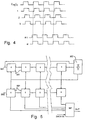
- the signals between the different delay elements are illustrated in the time chart in fig 4.
- the multiplexer also have a control word as input, and according to this control word the correct output is chosen.
- the multiplexer according to the invention preferably have a disable function, whereby a disable signal at a disable input can prevent any signal at the output. This is important in order to suppress a delay signal from the delay circuit, to e.g. prevent delayed signals from entering the next clock period, and so forth.
- the output from the multiplexer 303 is preferably forwarded through a pulse stretcher 305.
- the pulse stretcher makes the output pulses from the delay circuit longer in time. This reduces the sensitivity to noise.
- the delay value can be dynamically set by a delay control input (control word) to any value between 0 and N-1.
- any time period can be digitally represented by a binary word for the number of complete clock periods and a binary word for the additional delay as a number of 1/N fractions of a clock period.
- N is preferably controlled by an input port and can be optionally set to any of the values 50, 60 or 64.
- the set input is not shown in picture 1.
- the clock period can be exactly divided by 2, 3, 4, 5, 6, 8, 10, 12, 15, 16, 20, 25, 30, 32, 50, 60 and 64.
- the value can also be set to 72, and thereby provide for an exact division by 9, 18, 24, 36 and 72. This is of great importance in avoiding rounding errors.
- Other values that can be used for N are: 25, 30, 32, 36, 40, 72, 80, 100, 120 and 128. Still further values are naturally possible, as long as they provide for an exact division by numbers that are useful for the intended application, and preferably several different such numbers.
- the circuit is preferably designed with Emitter Coupled Logic (ECL) technology.
- ECL Emitter Coupled Logic
- the delay circuit of this embodiment also comprises a delay-locked loop with serially connected delay elements 301 and a phase comparator 302.
- the delay circuit according to this embodiment comprises a second set of serially connected delay elements 501, whereby the control signal from the phase comparator 302 is not only sent back to the delay elements 301 in the first set but also to the delay elements 501 in the second set.
- the delay elements 501 in the second set will have the same delay time values as the delay elements 301 in the first set (e.g. 2 ns per element).
- the first set may have a first input, IN1, and the second set another input, IN2.
- the second input signal which may be asynchronous with the first input signal (e.g. the clock signal), with delay time values that are automatically adjusted to the first input signal.
- the delay circuit according to the invention provides several advantages over the prior art, such as:
- An expected deviation for the circuit according to the invention is about +/- 170 ps, compared to +/- 1000 ps for analog circuits. This clearly illustrates the diminished need for tuning adjustments with the circuit according to the invention.
- the delay circuit of the invention accordingly provides a very exact division of the clock pulses, thereby producing a very exact time delay.
- the circuit also adapts to the clock signal, and is therefore always synchronized with the clock.
- the delay circuit described above may also be used for other purposes in the writing of lithographic patterns with raster scanning technique.
- the delay circuit may be used to delay the input clock signal of the electronic clock for certain logic components, such as components for adjusting the beam relative to other beams in the case of multiple beam writing, or components for fine adjustment placement of the whole pattern in the scanning direction.
Landscapes
- Physics & Mathematics (AREA)
- General Physics & Mathematics (AREA)
- Engineering & Computer Science (AREA)
- Multimedia (AREA)
- Signal Processing (AREA)
- Exposure And Positioning Against Photoresist Photosensitive Materials (AREA)
- Pulse Circuits (AREA)
- Exposure Of Semiconductors, Excluding Electron Or Ion Beam Exposure (AREA)
- Facsimile Scanning Arrangements (AREA)
- Lasers (AREA)
- Non-Silver Salt Photosensitive Materials And Non-Silver Salt Photography (AREA)
Abstract
Description
- The invention relates to a method and an apparatus for producing microlithography, in particular to the writing of photomasks for and direct writing of computer displays, microelectronic devices, and precision photo-etching, with the use of a time delay circuit such as is known from
European Patent EP 0 467 076, for example. It is also applicable to optical devices and a variety of electronic interconnection structures such as multichip modules. Other applications are possible, such as printing and graphics, as well as laser projection displays. - There is a development towards an ever-increasing number of features on photomasks, and increasingly sophisticated designs. For both computer displays, consumer TV screens and microelectronic products there is a rapid development towards at the same time larger sizes and smaller elemental cells. The development is most dramatic with semiconductor memories where a photomask could contain a billion elemental geometries or more.
- Another issue is the necessity of a small address grid. The writing system for semiconductor masks must be capable of writing features specified in units of 10 nm (nanometers) or less. It has been disclosed in
European Patent EP 0 467 076 by the same applicant that a combination of time delays and analog power modulation can be used to achieve an arbitrarily small address grid. The same patent also discloses the use of several beams and parallel data paths to increase the through-put of the writing system. - Naturally there is hereby a need for a very exact and reliable time delay circuit, something which has been a problem in the prior art which uses integrating delay circuits, creating the delay as the time needed to change an integrating capacitor to a determined level. There is also a problem with synchronization between the delay circuit and the clock pulse generator, and with complicated and time-consuming tuning adjustments, that is necessary in every new installation, and also when there have been changes in the clock rate etc.
- Further these known delay circuits are not fast enough in changing the time value, leading to a deterioration of the performance of the apparatus. The known delay circuits are also sensitive to interference.
- It is therefore an object with the present invention to provide an apparatus of the above mentioned type with an improved delay circuit.
- This object is fulfilled with an apparatus according to
claim 1. Other features and advantages with the present invention will be appreciated from the dependent claims, and from the following detailed description of a preferred embodiment of the invention with reference to the attached drawings. - The present invention relates to a method and apparatus for writing of lithographic patterns with raster scanning technique comprising the use of an electronic clock to control the modulation of the beam where the placement in the scanning directions of pattern elements is controlled by time delays of at least one clock signal by fractions of a clock period. The invention is characterised in that said clock period is divided into a number of equally spaced time values by means of a delay-locked loop and a particular time value is chosen according to a digital control word. Hereby several advantages are obtained, such as no need for tuning adjustments, an automatical adjustment to the clock and stability against interference.
- According to a preferred embodiment of the invention the delay circuit comprises N delay elements, each providing an additional delay of 1/N of the clock period, whereby N is digitally adjustable between at least two predetermined values, preferably 50, 60 and 64. Hereby the clock period can be exactly divided by several different numbers, diminishing the problem with rounding errors.
- According to another preferred embodiment of the invention the delay circuit comprises N delay elements, where N is a number such that N = 2n when n is an positive integer, whereby any time period can be digitally represented by a binary word for the number of complete clock periods and a binary word for the additional delay as a number of 1/N fractions of a clock period. Hereby any period of time becomes very easy to state and communicate.
- According to another preferred embodiment of the present invention the delay circuit is used for providing an address resolution significantly higher than what is given by the electronic clock, by time delay in the respective clock periods.
- According to still another preferred embodiment of the invention the delay circuit is used to delay the input clock signal of the electronic clock for certain logic components, such as components for adjusting the beam relative to other beams in the case of multiple beam writing, or components for fine adjustment of the placement of the whole pattern in the scanning direction.
-
- Figure 1 shows an apparatus for producing a surface pattern or structure according to the prior art.
- Figure 2 shows an embodiment of a modulator driver logic that can be used in the apparatus of fig 1.
- Figure 3 shows the delay circuit to be used in the invention according to a prefered embodiment.
- Figure 4 shows a time chart illustrating the operation for the delay circuit in fig 3.
- Figure 5 shows another embodiment of the delay circuit according to the invention.
-
- Reference will now be made to Fig. 1 showing an apparatus according to the prior art for producing surface patterns or structures on photosensitively coated supports or substrates. In the illustrated embodiment, the
substrate 3 is disposed on an object table 19 which is movable in the X- and Y-directions. A writing head with a focusinglens 15 and adeflector device 14 is arranged to be stationary in the X- and Y-directions. - A
laser beam source 13 produces a laser beam which is modulated in regard to its power and in particular its intensity by amodulator device 5. The focusinglens 15 focuses on the laser beam and forms a focused laser beam as indicated at 1, which is directed on to the surface of thesubstrate 3. - For monitoring the positioning of the object table 19, the apparatus has
position monitoring devices deflector device 14 and focusing lens 15). Together withelectric motors position monitoring devices - The servo mechanism produces
stripes 30 of a given width when thelaser beam 1 scans along thescan lines 2 in the X-direction at a constant speed. When arespective stripe 30 is completed, the X-servo mechanism performs a retrace stroke movement into the starting position and the object table 19 is then moved in the Y-direction by the width of a stripe by theelectric motor 17y. - The laser beam from the
source 13 is passed through the acousto-optical modulator 5 which is actuated by a high-frequencymodulation drive signal 4. Themodulation drive signal 4 is supplied by the modulator driver logic means 6. The intensity or power of themodulation drive signal 4 is controlled by an analog modulation drive signal of a digital-analog converter. The digital-analog converter which is disposed in the modulator driver stage or logic means 6, as shown in Fig. 3, is controlled by apower control signal 7 by way of a storage device which is preferably in the form of a register, for storage of the digital power control word required for producing the control effect. - Generally, the data delivery means includes a clock having a predetermined clock period between clock pulses, so as to establish a regular train of clock pulses. A data processing unit is provided for accepting input data and computing or establishing beam intensity data and beam position data for an edge in the pattern to be written. Both the beam intensity data and the beam position data are established in a digital format. The apparatus also includes as part of the data delivery means a signal processing unit for converting the beam position data to an equivalent time for positioning the laser beam along the scan line during scanning. Particularly, this equivalent time is converted as an integer number of clock pulses plus a fractional remainder. To create a time pulse corresponding to the equivalent time, digital counting means may be provided for generating a timing pulse at a time corresponding to the integer number of clock pulses and a time delay circuit may be provided for incurring to the timing pulse a time delay equal to the fractional remainder. Once the corresponding time pulse is created, a circuit may be used for setting the modulator input signal to the digital beam intensity data at the arrival of the timing pulse.
- Reference will be made at this point to Fig. 2 showing a preferred embodiment of the modulator drive logic means 6 described above with reference to Fig. 1. It has two storage devices for bit words, in the form of
registers register 605 is loaded with intensity orpower data 7 coming from thedata delivery device 24 shown in Fig. 1. Theregister 608 is loaded with position ordelay data 25 which also come from thedata delivery device 24. That takes place on the basis of a transition caused by theclock signal 31. In that arrangement, a digital-analog converter 606 is also operated by power data previously stored in thestorage device 607. It may also be in the form of a register. A digitally controlleddelay circuit 609 transfers theclock signal 31 to its output side, with a delay which depends on the data stored in theregister 608. After that delay the active edge of the clock signal is supplied at theoutput 610 of thedelay circuit 609. The value stored in theregister 605 is loaded into theregister 607 and passed to the input side of the digital-analog converter 606. After an internal delay in the digital-analog converter 606, a fresh analogpower control signal 4 occurs at the output of the modulator driver stage of the modulator device 5 (fig. 1). - In the prior art the delay circuits were digitally controlled analog delay circuits. These analog delay circuits have several drawbacks. For example the minimum time step is comparatively large, there is a strong need for individual adjustments to the clock, the latency period is significantly large, whereby there is a need for several delay circuits working by turns, there is a large sensitivity for external disturbances and the speed is very limited.
- In fig 3 there is shown a delay circuit according to the present invention. The delay circuit comprises a delayed-locked-loop, which in turn comprises N serially connected
delay elements 301, where N is an integer larger than two. Each delay elements delays a reference signal from the clock, with a quantum of time. This quantum of time is preferably the same for all the elements, i.e. 1/N of a clock period. Naturally the delay circuit can also comprise several delayed-locked loops. - The circuit also comprises a
phase comparator 302 connected to the output of the last delay element for receiving the routed delayed signal and the reference signal from the clock. Thereby thephase comparator 302 generates a control signal indicative of a difference between a phase of said routed delay signal and a phase of said reference signal. The output of the phase comparator is connected to said delay elements for transferring the control signal to the delay elements whereby each of the delay elements adjusts such that the phase of said reference signal is synchronized with the phase of said routed delay signal. That is, the delay circuit comprises a feedback system which automatically adjusts the amount of delay in each delay step. - Circuits using the delayed-locked-loop technique is known from e.g.
US patent 4 338 569. These known circuits have been used in completely different areas, though: adjustment of clock skew and time measurements (mainly in the area of nuclear physics and the like). - The delay circuit of the invention also comprises a selecting part, preferably comprising a multiplexer 303 being connected to the delay elements for receiving the delayed signals generated by the
delay elements 301 and to control the output of the delay circuit according to the desired fractional remainder. - To the input of the multiplexer 303 are connected the output signal from the respective delay elements. This is preferably accomplished with NAND-gates 304, such that the signal before and after each
delay element 301 are connected to a NAND-gate 304, the output of which is forwarded to the multiplexer 303. In this way the input signals to the multiplexer 303 are very short pulses. - The signals between the different delay elements are illustrated in the time chart in fig 4.
- The multiplexer also have a control word as input, and according to this control word the correct output is chosen. The multiplexer according to the invention preferably have a disable function, whereby a disable signal at a disable input can prevent any signal at the output. This is important in order to suppress a delay signal from the delay circuit, to e.g. prevent delayed signals from entering the next clock period, and so forth.
- The output from the multiplexer 303 is preferably forwarded through a pulse stretcher 305. The pulse stretcher makes the output pulses from the delay circuit longer in time. This reduces the sensitivity to noise.
- The delay value can be dynamically set by a delay control input (control word) to any value between 0 and N-1. N is preferably a number such that N = 2n where n is an positive integer. Hereby any time period can be digitally represented by a binary word for the number of complete clock periods and a binary word for the additional delay as a number of 1/N fractions of a clock period.
- Further, N is preferably controlled by an input port and can be optionally set to any of the values 50, 60 or 64. The set input is not shown in
picture 1. Hereby the clock period can be exactly divided by 2, 3, 4, 5, 6, 8, 10, 12, 15, 16, 20, 25, 30, 32, 50, 60 and 64. Possibly the value can also be set to 72, and thereby provide for an exact division by 9, 18, 24, 36 and 72. This is of great importance in avoiding rounding errors. Other values that can be used for N are: 25, 30, 32, 36, 40, 72, 80, 100, 120 and 128. Still further values are naturally possible, as long as they provide for an exact division by numbers that are useful for the intended application, and preferably several different such numbers. - The circuit is preferably designed with Emitter Coupled Logic (ECL) technology.
- In fig 5 there is shown an alternative embodiment of the delay circuit according to the invention. The delay circuit of this embodiment also comprises a delay-locked loop with serially connected
delay elements 301 and aphase comparator 302. However, the delay circuit according to this embodiment comprises a second set of serially connecteddelay elements 501, whereby the control signal from thephase comparator 302 is not only sent back to thedelay elements 301 in the first set but also to thedelay elements 501 in the second set. With this arrangement thedelay elements 501 in the second set will have the same delay time values as thedelay elements 301 in the first set (e.g. 2 ns per element). With this embodiment the first set may have a first input, IN1, and the second set another input, IN2. Hereby there is a possibility to delay the second input signal, which may be asynchronous with the first input signal (e.g. the clock signal), with delay time values that are automatically adjusted to the first input signal. - The delay circuit according to the invention provides several advantages over the prior art, such as:
- more stable and robust against interference;
- no need for tuning adjustments;
- automatically adjusts to the clock;
- can be made very compact;
- digitally controlled division;
- higher clock frequency;
- no latency or waiting periods in e.g. capacitors.
- For example, a clock with 50 Mhz provide a clock period T = 20 ns. If this period is to be divided by 60, the result is 333 ps per step. An expected deviation for the circuit according to the invention is about +/- 170 ps, compared to +/- 1000 ps for analog circuits. This clearly illustrates the diminished need for tuning adjustments with the circuit according to the invention.
- The delay circuit of the invention accordingly provides a very exact division of the clock pulses, thereby producing a very exact time delay. The circuit also adapts to the clock signal, and is therefore always synchronized with the clock.
- The delay circuit described above may also be used for other purposes in the writing of lithographic patterns with raster scanning technique. The delay circuit may be used to delay the input clock signal of the electronic clock for certain logic components, such as components for adjusting the beam relative to other beams in the case of multiple beam writing, or components for fine adjustment placement of the whole pattern in the scanning direction.
- The terms and expressions which have been employed in the foregoing specification are used therein as terms of description and not of limitation, and there is no intention in the use of such terms and expressions of excluding equivalents of the features shown and described or portions thereof, it being recognized that the scope of the invention is defined and limited only by the claims which follow.
Claims (22)
- Method for writing of lithographic patterns with raster scanning technique comprising the use of an electronic clock to control the modulation of the beam where the placement in the scanning directions of pattern elements is controlled by time delays by fractions of a clock period, characterised in that said clock is used to generate a number of preferably equally spaced delay time values by means of a delay-locked loop and a particular delay time value is chosen according to a digital control word.
- Method according to claim 1, where the digital control word is changed dynamically during the writing of a pattern.
- Method according to claim 1 or claim 2, characterised in that
said time delay circuit comprises a delayed-locked-loop, comprising:at least N serially connected delay elements, where N is an integer larger than two, each delaying a reference signal from said clock, with a quantum of time, anda phase comparator connected to the output of the N:th delay element for receiving the routed delayed signal and the reference signal, for generating a control signal indicative of the difference between a phase of said routed delay signal and a phase of said reference signal, and feedback means for transferring the control signal to the delay elements whereby each of the delay elements adjusts such that the phase of said reference signal is synchronized with the phase of said routed delay signal. - Method according to one of claims above, characterised in that said time delays are generated by a number of serially connected delay elements controlled by the control signal in the delayed-locked loop.
- Method according to claim 3, characterised in that the clock signal is connected to serially connected delay elements controlled by said control signal and selecting a number of delay elements to delay said clock signal to the output according to said digital control word.
- Method according to one of the claims above, characterised in that the delay circuit comprises N delay elements, each providing an additional delay of 1/N of the clock period, whereby N is digitally adjustable between at least two predetermined values, preferably chosen among the values 25, 30, 32, 36, 40, 50, 60, 64, 72, 80, 100, 120 and 128.
- Method according to one of the claims above, characterised in that the clock period is divided in N increments (steps), where N is a number such that N = 2n when n is a positive integer, whereby any time period can be digitally represented by a binary word for the number of complete clock periods and a binary word for the additional delay as a number of 1/N fractions of a clock period.
- Method according to one of the claims 1 to 7, characterised in that the delay circuit is used for providing an address resolution for pattern elements significantly higher than what is given by the electronic clock, by time delay in the respective clock periods.
- Method according to one of the claims 1 to 7, characterised in that the delay circuit is used to delay the input clock signal of the electronic clock for certain logic components.
- Method according to claim 9, characterised in that the logic components are components for adjusting the beam relative to other beams in the case of multiple beam writing.
- Method according to claim 9, characterised in that the logic components are components for fine adjustment placement of the whole pattern in the scanning direction.
- An apparatus adapted for writing of lithographic patterns with raster scanning technique, comprising an electronic clock and a time delay circuit, characterised in that the time delay circuit is a delayed-locked-loop circuit, driven by the said clock, whereby the output from the delay circuit is determined by input data.
- An apparatus according to claim 12, whereby it is intended for writing of complex patterns on a light sensitive surface by scanning at least one, by a modulator modulated, laser beam in parallel scan lines while moving along scan stripes in a direction perpendicular to the scan lines, the apparatus comprising:data delivery means for controlling the input of said modulator while the laser beam is scanning, wherein the.data delivery means includesa clock with a predetermined clock period between the clock pulses;a data processing unit for receiving input data and computing beam intensity data and beam position data each in digital format, for an edge in the pattern,a signal processing unit for converting the beam position data to an equivalent time for positioning the laser beam along the scan line during scanning, and converting this equivalent time to an integer number of clock pulses plus a fractional remainder, anda time delay circuitry to delay transition in the modulated data, producing said fractional remainder, for higher address resolution than corresponding to the data clock pulses.
- An apparatus according to claim 12 or 13, characterised in that
said time delay circuit comprises a delayed-locked-loop, comprising:N serially connected delay elements, where N is an integer larger than two, each delaying a reference signal from said clock, with a quantum of time,a phase comparator connected to the output of the N:th delay element for receiving the routed delayed signal and the reference signal, for generating a control signal indicative of a difference between a phase of said routed delay signal and a phase of said reference signal, and being feedback connected to said delay elements for transferring the control signal to the delay elements whereby each of the delay elements adjusts such that the phase of said reference signal is synchronized with the phase of said routed delay signal,a multiplexer being connected to the delay elements for receiving the delayed signals generated by the delay elements and to control the output of the delay circuit according to the desired fractional remainder. - An apparatus according to one of claim 12-14, characterised in that said time delays are generated by a number of serially connected delay elements controlled by the control signal in the delayed-locked loop.
- An apparatus according to claim 14, characterised in that the each delaying element delays the reference signal from said clock, with a quantum of time being 1/N of a clock period.
- An apparatus according to one of claim 12-16, characterised in that the delay circuit comprises N delay elements, each providing an additional delay of 1/N of the clock period, whereby N is digitally adjustable between at least two predetermined values, preferably chosen among the values 25, 30, 32, 36, 40, 50, 60, 64, 72, 80, 100, 120 and 128.
- An apparatus according to one of claim 12-17, characterised in that the delay circuit is produced with ECL (Emitter Coupled Logic) technology.
- An apparatus according to one of claim 12-17, characterised in that the delay circuit is produced with CMOS (Complementary Metal-Oxide Semiconductor) technology.
- An apparatus according to one of claim 12-19, characterised in that the apparatus provides an address resolution in pattern elements significantly higher than what is given by the electronic clock by means of a time delay from said delay circuit in the respective clock periods.
- An apparatus according to one of claim 12-19, characterised in that the apparatus is a multi-beam writer, where the delay circuit is adapted to delay the input clock signals of the electronic clock for adjusting a beam relative to the other beams.
- An apparatus according to one of claim 12-19, characterised in that the delay circuit is used to delay the input clock signals of the electronic clock for fine adjustment of the placement of the whole pattern in the writing direction.
Applications Claiming Priority (3)
| Application Number | Priority Date | Filing Date | Title |
|---|---|---|---|
| SE9703700A SE511189C2 (en) | 1997-10-13 | 1997-10-13 | Method and apparatus for a laser printer for complex microlithographic patterns with a delay circuit |
| SE9703700 | 1997-10-13 | ||
| PCT/SE1998/001835 WO1999019772A1 (en) | 1997-10-13 | 1998-10-13 | Apparatus for a laser writer for complex microlithographic patterns with a delay circuit |
Publications (2)
| Publication Number | Publication Date |
|---|---|
| EP1023638A1 EP1023638A1 (en) | 2000-08-02 |
| EP1023638B1 true EP1023638B1 (en) | 2004-04-21 |
Family
ID=20408569
Family Applications (1)
| Application Number | Title | Priority Date | Filing Date |
|---|---|---|---|
| EP98950562A Expired - Lifetime EP1023638B1 (en) | 1997-10-13 | 1998-10-13 | Apparatus for a laser writer for complex microlithographic patterns with a delay circuit |
Country Status (7)
| Country | Link |
|---|---|
| EP (1) | EP1023638B1 (en) |
| JP (1) | JP2001520407A (en) |
| AT (1) | ATE265058T1 (en) |
| AU (1) | AU9657098A (en) |
| DE (1) | DE69823375T2 (en) |
| SE (1) | SE511189C2 (en) |
| WO (1) | WO1999019772A1 (en) |
Families Citing this family (1)
| Publication number | Priority date | Publication date | Assignee | Title |
|---|---|---|---|---|
| US8941085B2 (en) | 2013-03-14 | 2015-01-27 | Taiwan Semiconductor Manufacturing Company, Ltd. | Electron beam lithography systems and methods including time division multiplex loading |
Family Cites Families (2)
| Publication number | Priority date | Publication date | Assignee | Title |
|---|---|---|---|---|
| US4549222A (en) * | 1982-03-04 | 1985-10-22 | Ing. C. Olivetti & C., S.P.A. | Dot matrix printing method and printer therefor |
| US5635976A (en) * | 1991-07-17 | 1997-06-03 | Micronic Laser Systems Ab | Method and apparatus for the production of a structure by focused laser radiation on a photosensitively coated substrate |
-
1997
- 1997-10-13 SE SE9703700A patent/SE511189C2/en not_active IP Right Cessation
-
1998
- 1998-10-13 WO PCT/SE1998/001835 patent/WO1999019772A1/en not_active Ceased
- 1998-10-13 JP JP2000516261A patent/JP2001520407A/en not_active Ceased
- 1998-10-13 EP EP98950562A patent/EP1023638B1/en not_active Expired - Lifetime
- 1998-10-13 DE DE69823375T patent/DE69823375T2/en not_active Expired - Fee Related
- 1998-10-13 AU AU96570/98A patent/AU9657098A/en not_active Abandoned
- 1998-10-13 AT AT98950562T patent/ATE265058T1/en not_active IP Right Cessation
Also Published As
| Publication number | Publication date |
|---|---|
| JP2001520407A (en) | 2001-10-30 |
| EP1023638A1 (en) | 2000-08-02 |
| DE69823375T2 (en) | 2005-05-04 |
| WO1999019772A1 (en) | 1999-04-22 |
| SE9703700D0 (en) | 1997-10-13 |
| AU9657098A (en) | 1999-05-03 |
| ATE265058T1 (en) | 2004-05-15 |
| SE511189C2 (en) | 1999-08-23 |
| DE69823375D1 (en) | 2004-05-27 |
| SE9703700L (en) | 1999-04-14 |
Similar Documents
| Publication | Publication Date | Title |
|---|---|---|
| EP0956516B1 (en) | Method and apparatus for the production of a structure by focused laser radiation on a photosensitively coated substrate | |
| RU2257603C2 (en) | Device for forming images | |
| US7088468B1 (en) | Data-conversion method for a multibeam laser writer for very complex microlithographic patterns | |
| US5635976A (en) | Method and apparatus for the production of a structure by focused laser radiation on a photosensitively coated substrate | |
| US7050080B2 (en) | Image forming apparatus for controlling image writing by adjusting image clock | |
| US20130250263A1 (en) | Pulsed Laser Source with High Repetition Rate | |
| US20240255864A1 (en) | Image forming apparatus that scans photosensitive member using plurality of scan beams | |
| EP1023638A1 (en) | Apparatus for a laser writer for complex microlithographic patterns with a delay circuit | |
| US6590599B2 (en) | Apparatus and method for equivalently changing a write clock frequency | |
| CN108873620B (en) | Method for improving energy uniformity in direct-writing photoetching machine | |
| US20090284788A1 (en) | Image forming apparatus and control method thereof | |
| JPH1155477A (en) | Image forming apparatus and method | |
| US5206664A (en) | Recording apparatus using semiconductor laser | |
| US20060103712A1 (en) | Multi-beam image output apparatus and method | |
| CN1166984C (en) | Method and apparatus for fabricating structures on photosensitive coated substrates using focused laser radiation | |
| JP3276296B2 (en) | Laser writing system with straightness correction function for pixel array | |
| JPS59181615A (en) | Luster type beam drawing device | |
| JPH1080781A (en) | Laser writing system with pixel array correction function |
Legal Events
| Date | Code | Title | Description |
|---|---|---|---|
| PUAI | Public reference made under article 153(3) epc to a published international application that has entered the european phase |
Free format text: ORIGINAL CODE: 0009012 |
|
| 17P | Request for examination filed |
Effective date: 20000407 |
|
| AK | Designated contracting states |
Kind code of ref document: A1 Designated state(s): AT CH DE GB LI |
|
| GRAP | Despatch of communication of intention to grant a patent |
Free format text: ORIGINAL CODE: EPIDOSNIGR1 |
|
| GRAS | Grant fee paid |
Free format text: ORIGINAL CODE: EPIDOSNIGR3 |
|
| GRAA | (expected) grant |
Free format text: ORIGINAL CODE: 0009210 |
|
| AK | Designated contracting states |
Kind code of ref document: B1 Designated state(s): AT CH DE GB LI |
|
| PG25 | Lapsed in a contracting state [announced via postgrant information from national office to epo] |
Ref country code: LI Free format text: LAPSE BECAUSE OF FAILURE TO SUBMIT A TRANSLATION OF THE DESCRIPTION OR TO PAY THE FEE WITHIN THE PRESCRIBED TIME-LIMIT Effective date: 20040421 Ref country code: CH Free format text: LAPSE BECAUSE OF FAILURE TO SUBMIT A TRANSLATION OF THE DESCRIPTION OR TO PAY THE FEE WITHIN THE PRESCRIBED TIME-LIMIT Effective date: 20040421 Ref country code: AT Free format text: LAPSE BECAUSE OF FAILURE TO SUBMIT A TRANSLATION OF THE DESCRIPTION OR TO PAY THE FEE WITHIN THE PRESCRIBED TIME-LIMIT Effective date: 20040421 |
|
| REG | Reference to a national code |
Ref country code: GB Ref legal event code: FG4D |
|
| REG | Reference to a national code |
Ref country code: CH Ref legal event code: EP |
|
| REF | Corresponds to: |
Ref document number: 69823375 Country of ref document: DE Date of ref document: 20040527 Kind code of ref document: P |
|
| PG25 | Lapsed in a contracting state [announced via postgrant information from national office to epo] |
Ref country code: GB Free format text: LAPSE BECAUSE OF NON-PAYMENT OF DUE FEES Effective date: 20041013 |
|
| REG | Reference to a national code |
Ref country code: CH Ref legal event code: PL |
|
| PLBE | No opposition filed within time limit |
Free format text: ORIGINAL CODE: 0009261 |
|
| STAA | Information on the status of an ep patent application or granted ep patent |
Free format text: STATUS: NO OPPOSITION FILED WITHIN TIME LIMIT |
|
| 26N | No opposition filed |
Effective date: 20050124 |
|
| PG25 | Lapsed in a contracting state [announced via postgrant information from national office to epo] |
Ref country code: DE Free format text: LAPSE BECAUSE OF NON-PAYMENT OF DUE FEES Effective date: 20050503 |
|
| GBPC | Gb: european patent ceased through non-payment of renewal fee |
Effective date: 20041013 |