EP1022729A2 - Disk player - Google Patents
Disk player Download PDFInfo
- Publication number
- EP1022729A2 EP1022729A2 EP00100284A EP00100284A EP1022729A2 EP 1022729 A2 EP1022729 A2 EP 1022729A2 EP 00100284 A EP00100284 A EP 00100284A EP 00100284 A EP00100284 A EP 00100284A EP 1022729 A2 EP1022729 A2 EP 1022729A2
- Authority
- EP
- European Patent Office
- Prior art keywords
- receiving area
- recording
- signal
- prepit
- difference
- Prior art date
- Legal status (The legal status is an assumption and is not a legal conclusion. Google has not performed a legal analysis and makes no representation as to the accuracy of the status listed.)
- Withdrawn
Links
Images




Classifications
-
- G—PHYSICS
- G11—INFORMATION STORAGE
- G11B—INFORMATION STORAGE BASED ON RELATIVE MOVEMENT BETWEEN RECORD CARRIER AND TRANSDUCER
- G11B7/00—Recording or reproducing by optical means, e.g. recording using a thermal beam of optical radiation by modifying optical properties or the physical structure, reproducing using an optical beam at lower power by sensing optical properties; Record carriers therefor
- G11B7/004—Recording, reproducing or erasing methods; Read, write or erase circuits therefor
- G11B7/005—Reproducing
- G11B7/0051—Reproducing involving phase depth effects
-
- G—PHYSICS
- G11—INFORMATION STORAGE
- G11B—INFORMATION STORAGE BASED ON RELATIVE MOVEMENT BETWEEN RECORD CARRIER AND TRANSDUCER
- G11B7/00—Recording or reproducing by optical means, e.g. recording using a thermal beam of optical radiation by modifying optical properties or the physical structure, reproducing using an optical beam at lower power by sensing optical properties; Record carriers therefor
- G11B7/004—Recording, reproducing or erasing methods; Read, write or erase circuits therefor
- G11B7/005—Reproducing
-
- G—PHYSICS
- G11—INFORMATION STORAGE
- G11B—INFORMATION STORAGE BASED ON RELATIVE MOVEMENT BETWEEN RECORD CARRIER AND TRANSDUCER
- G11B7/00—Recording or reproducing by optical means, e.g. recording using a thermal beam of optical radiation by modifying optical properties or the physical structure, reproducing using an optical beam at lower power by sensing optical properties; Record carriers therefor
- G11B7/08—Disposition or mounting of heads or light sources relatively to record carriers
- G11B7/09—Disposition or mounting of heads or light sources relatively to record carriers with provision for moving the light beam or focus plane for the purpose of maintaining alignment of the light beam relative to the record carrier during transducing operation, e.g. to compensate for surface irregularities of the latter or for track following
- G11B7/0941—Methods and circuits for servo gain or phase compensation during operation
Definitions
- the present invention relates to a disk player for reproducing or recording recording information from or onto a disk type information recording medium with high recording density which is represented by DVD.
- a disk type information recording medium is DVD-Rewritable (hereinafter, referred to as DVD-RW) onto which the recording information can be written and where prepits are previously formed as various control information such as address information.
- a disk type information recording medium such as DVD-RW
- prepits are formed in advance on the disk as preformed information which indicates various control information such as address information
- the prepits are detected so that necessary control information can be obtained.
- an information pit is formed on a groove track by changing reflectance in accordance with a crystal state or non-crystal state, and a prepit is previously formed on a land track as an uneven phase pit.
- 4-divided light receiving elements are frequently used in order to realize focusing servo by means of astigmatism and tracking servo by means of push-pull.
- the 4-divided light receiving elements are also used for the detection of the prepits.
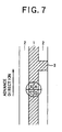
- a reflected light of a beam spot emitted onto the groove track 1 is divided into four areas A through D by the light receiving elements so that respective detection signals are obtained, and a prepit 3 formed on the land track 2 is detected by obtaining (A-B) + (D-C) .
- the arrow in FIG. 7 shows the advance direction of the groove track 1.
- the advance direction of a light beam is opposite to the direction shown by the arrow in FIG. 7.
- a delay of the detection signals due to a property of the phase pit should be taken into consideration.
- a disk type information recording medium such as DVD-R (DVD-Recordable)
- an information pit and a prepit are formed by making a substrate uneven so that a phase difference is given to the light beam, and the intensity of the light modulated by diffraction on the pit is detected. Therefore, because of a difference in properties such as diffraction efficiency and diffraction angle at the phase pits, detection timing varies in the respective areas of the light receiving elements.
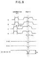
- FIG. 8 shows a conventional method of detecting the prepits using the conventional 4-divided light receiving elements.
- the detection timing of the information pit in the areas A and B is delayed from the detection timing in the areas C and D by ⁇ t1.
- the detection timing of the prepit since a beam spot is on the groove track and the prepit is on the land track, diffraction property becomes complicated, and thus changes are made in the areas B and D earlier and changes in the areas A and C are delayed by ⁇ t2.
- the changes in the areas A and D are made in a direction where the light intensity is weakened, and the changes in the areas B and C are made in a direction where the light intensity is strengthen.
- m1 in the drawing is a prepit detecting range and is to be a detection margin.
- a threshold is set suitably within the range of m1 so that the prepit is read.
- the prepit detecting range m1 to be obtained must be larger.
- actually peaks of the changed portions due to the prepit do not coincide with each other because of the delay time ⁇ t2, and thus m1 becomes smaller.
- prepit detecting accuracy is restricted and an influence of malfunction due to a noise becomes great accordingly.
- the delay time ⁇ t2 fluctuates depending on a cutting condition or the like of the prepit on the optical disk, it is not easy to predict an amount of the delay ⁇ t2.
- a disk player in accordance with the present invention is an apparatus for recording or reproducing recording information to a recording disk by emitting a light beam onto the recording disk.
- the recording disk has a recording track for recording the recording information, a guide track for guiding the light beam to the recording track, and a prepit which is pre-formed on the guiding track and which serves as control information for controlling a recording operation or a reproduction operation of the disk player.
- the disk player includes a light receiving device that receives the light beam reflected by the recording disk and that has a light receiving surface in which a first receiving area, a second receiving area, a third receiving area and a forth receiving area are formed.
- the first receiving area and the second receiving area are located in a back area of the light receiving surface with respect to an advance direction of a relative movement of the light beam with respect to the recording track.
- the third receiving area and the fourth receiving area are located in a front area of the light receiving surface with respect to the advance direction of the movement of the light beam.
- the first receiving area and the fourth receiving area are located near the guide track on which the prepit is formed, as compared with locations of the second receiving area and the third receiving area.
- the disk player further includes a first generating device that generates a first difference signal indicating a difference between a first detection signal generated by the light beam that is received in the first receiving area and a third detection signal generated by the light beam that is received in the third receiving area; a second generating device that generates a second difference signal indicating a difference between a second detection signal generated by the light beam that is received in the second receiving area and a fourth detection signal generated by the light beam that is received in the fourth receiving area; and a phase difference detection device that detects a phase difference between the first difference signal and the second difference signal.
- the reflected light beam is received by the light receiving device having four receiving areas. Namely, the reflected light beam is received by the first receiving area, the second receiving area, the third receiving area and the fourth receiving area. Since the locations of the respective four receiving areas are different, the light beam is received in such a way that the light beam is divided into four parts.
- the change in the light beam occurs. This change is received by the respective four receiving areas. Because the locations of the respective receiving areas are different from each other, the timing and the direction of the change of the light beam caused by the prepit is different among the four receiving area.
- the four detection signals In response to the reception of the light beam, four detection signals, namely, the first through fourth detection signals are generated.
- the four detection signals correspond to the four receiving areas, respectively.
- the change of the light beam caused by the prepit appears as a level change of each detection signal. Because of the difference of the locations of the respective receiving areas, the timing and the direction of the level change is different among the four detection signal.
- the first detection signal and the third detection signal coincide with each other, and the second detection signal and the fourth detection signal coincide with each other.
- the first detection signal and the third detection signal are opposite to each other, and the second detection signal and the fourth detection signal are opposite to each other.
- the first difference signal which indicates the difference between the first detection signal and the third detection signal and the second difference signal which indicates the difference between the second detection signal and the fourth detection signal are generated.
- the level change caused by the prepit in the first detection signal and the third detection signal more clearly appears in the first difference signal.
- the level change caused by the prepit in the second detection signal and the fourth detection signal more clearly appears in the second difference signal.
- the phase difference detection device detects this phase difference.
- the time difference between the first difference signal and the second difference signal can be compensated for each of individual recording disks. Accordingly, even if the manufacturing conditions of individual recording disks are different, the accurate phase difference can be detected, and, for example, the accuracy of the compensation of the time difference between the first difference signal and the second difference signal can be improved.
- a compensating device and a prepit signal generating device may be added.
- the compensating device is a device for generating a compensation signal by delaying the second difference signal by a delay time determined on the basis of the phase difference.
- the prepit signal generating device is a device for generating a prepit signal by adding the first difference signal to the compensation signal.
- the difference in the timings of the level changes caused by the prepit between the first difference signal and the second difference signal is compensated by delaying the second difference signal in such a way that the timings of the level changes in the both signals coincide with each other.
- the prepit signal is generated by adding the first difference signal and the delayed second difference signal (i.e., the compensation signal). Because the timings of the level changes caused by the prepit in the first difference signal and the delayed second difference signal coincide with each other, the level change of the first difference signal and the level change of the delayed second difference signal are effectively added. Therefore, the large level change corresponding to the change of the light beam caused by the prepit appears in the prepit signal. Accordingly, even if noise is contained in the prepit signal, it is easy to distinguish the level change corresponding to the change of the light beam caused by the prepit from the noise. Therefore, the accuracy of the prepit detection can be improved.
- the compensating device may include: a control voltage setting device that sets a control voltage proportional to the phase difference; and a voltage control delay device that delays the second difference signal by a delay time corresponding to the control voltage.
- a control voltage setting device that sets a control voltage proportional to the phase difference
- a voltage control delay device that delays the second difference signal by a delay time corresponding to the control voltage.
- the phase difference detection device may detect the phase difference, while a detection of a recording mark formed on the recording track is not carried out. While the detection of the recording mark is carried out, the reflected light beam is relatively weak, and thus, it is difficult to detect the phase difference. Because of this reason, the phase difference detection is carried out, while the detection of the recording mark is not carried out. Therefore, the performance of the detection of the phase difference can be improved.
- the division of the respective four receiving areas in the light receiving surface of the light receiving device may be determined as follows.
- the back area of the light receiving surface is divided into the first receiving area and the second receiving area by a first division line.
- the front area of the light receiving surface is divided into the third receiving area and the fourth receiving area by the first division line.
- the light receiving surface is divided into the back area and the front area by a second division line.
- the first division line is approximately parallel to the recording track.
- the second division line is perpendicular to the first division line. The intersection of the first division line and the second division line is located within the light receiving surface.
- a delay device that delays a first difference signal may be added.
- DVD-RW DVD-Rewritable
- FIG. 1 is a block diagram mainly showing a configuration of the prepit detection circuit in the disk player according to the first embodiment.
- the prepit detection circuit includes subtracters 10 and 11, a voltage control delay line 12, an adder 13, comparators 14 and 15, a phase comparator 16, a pulse width voltage converter 17, a sample-hold portion 18, a control voltage adjusting portion 19 and a 14T space detector 20.
- the 4-divided light receiving elements divide a reflected light of a light beam emitted onto a disk into four areas A, B C and D so as to receive them. Detection signals of the reflected lights are output from the divided areas A through D so as to be input into the prepit detection circuit.
- the binarized RF signals are input into the prepit detection circuit.
- FIG. 2 shows waveform patterns when a prepit 3 on a land track 2 is detected on a portion where an information pit of a groove track 1 does not exist.
- signal levels in the areas B and D which change earlier change.
- Signal levels in the areas A and C which change later delay by delay time ⁇ t relative to B and D, and the signal levels change.
- the delay time ⁇ t is caused by a difference in a diffraction property based on a phase difference between the light beams.
- light intensity in the areas A through D changes due to the prepit 3 similarly to the case of FIG. 8.
- the signal levels in A through D change at the same timing, and directions and amounts of the change in the signal levels are equal to each other. For this reason, the changed portion due to the information pit is canceled when subtractions are made according to A-C and D-B as mentioned later.
- the signal levels in A through D change due to the information pit at the same timing because in DVD-RW the information pit is not a phase pit and a recording film detects a change in reflectance which varies according to a crystal state or non-crystal state using phase change recording. For this reason, the above-mentioned detection delay does not occur.
- the detection signals in the areas A and C are input into the subtracter 10.
- a difference of the detection signals in A and C is obtained in the subtracter 10 and a differential signal corresponding to A-C is output.
- the differential signal A-C changes in a pattern shown in FIG. 2. Namely, a waveform pattern that the signal level is lowered according to the prepit 3 is obtained.
- the detection signals in the areas B and D are input into the subtracter 11.
- a difference of the detection signals in B and D is obtained in the subtracter 11 and a differential signal corresponding to D-B is output.
- the differential signal D-B changes in a pattern shown in FIG. 2. Also in this case, a waveform pattern that the signal level is lowered according to the prepit 3 is obtained.
- the prepit detection circuit corrects the delay in the peaks according to a process mentioned later, so as to suitably cancel the delay time ⁇ t.
- the differential signal D-B output from the subtracter 11 is input into the voltage control delay line 12.
- the input differential signal D-B is held for delay time which is determined according to a control voltage, and a correction signal (D-B)' which is shifted by the delay time is output.
- the voltage control delay line 12 is a device for applying a control voltage from the outside and holding a signal by delay time which is substantially proportional to the control voltage so as to output the signal.
- a device is on the market in a form of IC.
- it is enough that assumed delay time ⁇ t is within a range that the delay time of the voltage control delay line 12 can be controlled.
- the differential signal A-C output from the subtracter 10 is input into the comparator 14, and the differential signal D-B output from the subtracter 11 is input into the comparator 15.
- a constant reference voltage Vref is connected with a plus-side input terminal, and the differential signals A-C and D-B are binarized respectively by threshold values corresponding to the reference voltages Vref so as to be output.
- the binarized output is held low, but the signal level is less than the threshold value at timing T0 after the prepit 3 is started to be detected. For this reason, the binarized output becomes high.
- the binarized output of the differential signal A-C changes similarly, but timing T1 that the binarized output becomes high is delayed by the delay time ⁇ t from the timing T0. Only this point is different from that of the differential signal D-B.
- phase difference pulse which becomes high from the rising of the binarized output of the differential signal D-B to the rising of the binarized output of the differential signal A-C, is output from the phase comparator 16.
- the phase difference pulse shows a waveform pattern having a pulse width of the delay time ⁇ t.
- the phase difference pulse output from the phase comparator 16 is input into the pulse width voltage converter 17.
- the phase difference pulse is integrated so that an integral output having a level in proportion to the pulse width is generated.
- the integral output from the pulse width voltage converter 17 is input into the sample-hold portion 18 so as to be held at a level of an integral output at which a sample pulse, mentioned later, is input.
- FIG. 3 is a diagram showing a concrete circuit configuration of the pulse width voltage converter 17 and the sample-hold portion 18. As shown in FIG. 3, the whole circuit includes a constant-current source 30, a first switch portion 31, a second switch portion 32, a capacitor 33, an operational amplifier 34, a third switch portion 35, a hold capacitor 36 and an operational amplifier 37.
- a charging current is supplied to the capacitor 33 via the first switch portion 31 by the constant-current source 30 whose one terminal is connected with a power source.
- the first switch portion 31 is turned ON, and a constant current flows from the constant-current source 30 so that the capacitor 33 is charged.
- a voltage of a plus-side input terminal of the operational amplifier 34 rises linearly, and voltages of a minus-side input terminal with the same potential and output terminal also rise linearly.
- the waveform of the integral output of the operational amplifier 34 changes as shown in FIG. 2.
- the second switch portion 32 When a reset pulse is changed from low into high, the second switch portion 32 is turned ON. One terminal of the second switch portion 32 is connected with the plus-side input terminal of the operational amplifier 34 and the other terminal is connected with a ground. Therefore, when the second switch portion 32 is turned ON, the input and output of the operational amplifier 34 can be lowered to a ground potential.
- the reset pulse is applied at suitable timing so that the integral output of the pulse width voltage converter 17 is reset.
- the reset pulse may be output by CPU or the like, or the reset pulse may be generated from a sample pulse output from the 14T space detector 20.
- a charging current is supplied to the hold capacitor 36 via the third switch portion 35 by the integral output from the operational amplifier 34.
- the third switch portion 35 is turned ON, and a current flows from the operational amplifier 34 so that the hold capacitor 36 is charged.
- the voltages at respective points of the operational amplifier 37 become equal to those of the operational amplifier 34.
- the sample pulse becomes low so that the third switch portion 35 is turned OFF, the voltage state of the operational amplifier 37 at that time is held.
- a signal whose level is in proportion to the pulse width of the phase difference pulse, is output from the operational amplifier 37.
- the above-mentioned sample pulse is generated by the 14T space detector 20.
- the 14T space detector 20 detects existence of a 14T space in a SYNC pattern of the disk based on the binarized RF signal, and generates a corresponding sample pulse so as to output the generated pulse into the sample-hold portion 18. Namely, as shown in FIG. 2, since a pulse, which becomes high only for constant time width according to the 14T space, can be obtained based on the binarized RF signal, the 14T space can be detected based on the pulse width.
- the control voltage of the voltage control delay line 12 can be obtained based on the prepit 3 positioned in the 14T space on the disk.
- the delay time ⁇ t is set based on the prepit 3 positioned in the 14T space. This is due to the following reasons. Namely, in the position of a recording mark on the disk, a returned light amount is reduced due to the pit corresponding to the recording mark and thus the signal level becomes low on the prepit 3 positioned around the recording mark, and detecting performance is deteriorated.
- the 14T space has a comparatively long range of unrecorded area, a returned light amount is sufficiently large so that the signal level of the prepit positioned therearound is held high.
- the 14T space is advantageous to the detecting performance. For this reason, a phase difference is detected in the position of the 14T space in the above manner so that the process thereafter is executed satisfactorily.
- an output pulse from the sample-hold portion 18 is input into the control voltage adjusting portion 19.
- the control voltage adjusting portion 19 amplifies the output pulse from the sample-hold portion 18 by a specified gain and adds a specified DC offset thereto so as to generate a control voltage which is matched with the property of the voltage control delay line 12.
- the control voltage is applied to the voltage control delay line 12 so that the delay time ⁇ t, which accurately corresponds to the phase difference between two differential signals, is set.
- the differential signals D-B input into the voltage control line 12 is held for the delay time ⁇ t set in the above manner so as to be output as a correction signal (D-B)'. Then, the differential signal A-C output from the subtracter 10 and the correction signal (D-B)' output from the voltage control delay line 12 are input into the adder 13. In the adder 13, the differential signal A-C is added to the correction signal (D-B)' so that a prepit detection signal (A-C) + (D-B)' is output.
- the differential signal A-C and the correction signal (D-B)' show the same change pattern with respect to the prepit 3, and their changes are made at the same timing and their peaks coincide with each other. Therefore, the prepit detection signal (A-C) + (D-B)' output from the adder 10 also changes at the same timing as of the differential signal A-C and the correction signal (D-B)', and its peak appears with a size which is double the size of the differential signal A-C and the correction signal (D-B)'.
- the prepit detecting range m is larger than the prepit detecting range m1 which is in the conventional case of detecting the prepit shown in FIG. 8.
- the prepit 3 is determined by whether the prepit 3 exceeds the threshold.
- the wider prepit detecting range m is, the more sufficiently a detection margin is secured. For this reason, a fluctuation in the detection signal level does not influence the detection so much. Therefore, in the case where the prepit detection circuit is constituted according to the first embodiment, even when the detection signal, which is the same as that of the conventional prepit detection circuit, is used, the detecting accuracy is high and satisfactory detecting performance can be obtained.
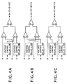
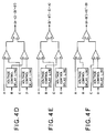
- FIGS. 4A through 4I show variations which are different from FIG. 1 as the configuration of the prepit detection circuit.
- FIGS. 4A through 4I in order to simplify the configuration, only the adder, subtracter and voltage control delay line are shown.
- the prepit circuit can be constituted as shown in FIGS. 4A through 4I.
- the prepit detection signal obtained as the output is equivalent to the prepit detection signal (A-C) + (D-B)' of FIG. 1 with respect to obtaining the large prepit detection range, and the prepit can be detected in the similar manner.
- FIG. 5 is a block diagram corresponding to FIG. 1 showing the prepit detection circuit of the disk player according to the second embodiment.
- the same reference numerals are given to the components same as those in FIG. 1, and the description thereof will be omitted.
- a fixed delay line 21 is additionally provided between the subtracter 10 and the comparator 14, and the output of the subtracter 11 is not connected with the comparator 15.
- the output of the voltage control delay line 12 is connected with the comparator 15.
- FIG. 6 is a diagram showing waveform patterns of the respective portions of the prepit detection circuit according to the second embodiment.
- FIG. 6 is similar to FIG. 2 except that a correction signal (A-C)' output from the fixed delay line 21 is added and the timing of the respective signals is slightly different from each other. Therefore, in FIG. 6, the description about the points same as those in FIG. 2 will be omitted.
- A-C correction signal
- the differential signal A-C output from the subtracter 10 is input into the fixed delay line 21.
- the fixed delay line 21 holds the differential signal A-C for delay time ⁇ T as a specified fixed value so as to output a delayed correction signal (A-C)'.
- the fixed delay line 21 cannot change delay time unlike the aforementioned voltage control delay line 12, and thus the preset delay time ⁇ T is used fixedly.
- the correction signal (A-C)' output from the fixed delay line 21 is input into the comparator 14. Meanwhile, the correction signal (D-B)' output from the voltage control delay line 12 is input into the comparator 15. Therefore, as shown in FIG. 6, the correction signal (A-C)' and the correction signal (D-B)' are binarized so as to be output respectively from the comparators 14 and 15.
- a phase difference pulse output from the phase comparator 16 becomes high from the rising of the binarized output of the correction signal (D-B)' to the rising of the binarized output of the correction signal (A-C)'.
- a pulse width of the phase difference pulse substantially coincides with the delay time ⁇ T of the fixed delay line 21.
- the fixed delay line 21 when the fixed delay line 21 is not provided, the phase of the differential signal (A-C) coincides with the phase of the correction signal (D-B)', and thus a relationship between the phases is not fixed so that a suitable phase difference pulse cannot be obtained.
- the fixed delay line 21 is provided in order to give a fixed bias to the phase relationship.
- the pulse width voltage converter 17, the sample-hold portion 18, the control voltage adjusting portion 19 and the 14T space detector 20 execute the process in the similar manner to that in the first embodiment so that a control voltage for the voltage control delay line 12 is generated.
- the differential signal A-C and the correction signal (D-B)' are added to each other so that the prepit detection signal (A-C) + (D-B)' is output.
- the phase difference pulse is obtained after being delayed by the delay time ⁇ t, the detection in the phase difference is fed back. Therefore, although responsibility which is equal to that of the first embodiment cannot be obtained, even in the case where a shift of the phase difference pulse occurs due to an influence of noise or the like, the shift is corrected automatically. As a result, the prepit can be detected without being influenced by an external noise.
- the phase difference which is caused by the shift in the prepit detection timing in the respective divided areas of the light receiving elements, is detected, and delay time is obtained based on the phase difference so that the prepit detection signal is obtained.
- the prepit detecting range m is obtained for the prepit 3 formed as a phase pit so that a large detection margin is secured. Therefore, possibility of misdetection of the prepit 3, which is caused by a fluctuation of the detection signal due to a nose or the like, is reduced.
- the phase difference fluctuates according to cutting conditions of the prepit 3
- the accurate phase difference is always detected so that the prepit can be detected with high accuracy.
- the present invention can be applied to a disk type information recording medium where an information pit is recorded by a change in reflectance and the prepit 3 is formed as a phase pit.
Landscapes
- Optical Recording Or Reproduction (AREA)
Abstract
Description
Claims (8)
- A disk player for recording or reproducing recording information to a recording disk by emitting a light beam onto the recording disk, the recording disk having a recording track (1) for recording the recording information, a guide track (2) for guiding the light beam to the recording track, and a prepit (3) which is pre-formed on the guiding track and which serves as control information for controlling a recording operation or a reproduction operation of the disk player, characterised in that the disk player comprises:a light receiving device that receives the light beam reflected by the recording disk and that has a light receiving surface in which a first receiving area (A), a second receiving area (B), a third receiving area (C) and a forth receiving area (D) are formed, the first receiving area and the second receiving area being located in a back area of the light receiving surface with respect to an advance direction of a relative movement of the light beam with respect to the recording track, the third receiving area and the fourth receiving area being located in a front area of the light receiving surface with respect to the advance direction of the movement of the light beam, the first receiving area and the fourth receiving area being located near the guide track on which the prepit is formed, as compared with locations of the second receiving area and the third receiving area;a first generating device (10) that generates a first difference signal indicating a difference between a first detection signal generated by the light beam that is received in the first receiving area and a third detection signal generated by the light beam that is received in the third receiving area;a second generating device (11) that generates a second difference signal indicating a difference between a second detection signal generated by the light beam that is received in the second receiving area and a fourth detection signal generated by the light beam that is received in the fourth receiving area; anda phase difference detection device (14-18, 20) that detects a phase difference between the first difference signal and the second difference signal.
- The disk player according to claim 1 further comprising:a compensating device (12, 19) that generates a compensation signal by delaying the second difference signal by a delay time determined on the basis of the phase difference; anda prepit signal generating device (13) that generates a prepit signal by adding the first difference signal to the compensation signal.
- The disk player according to claim 2, wherein the compensating device (12, 19) comprises:a control voltage setting device (19) that sets a control voltage proportional to the phase difference; anda voltage control delay device (12) that delays the second difference signal by a delay time corresponding to the control voltage.
- The disk player according to claim 2 or 3, wherein the compensating device (12, 19) delays the second difference signal such that a peak position of the second difference signal coincides with a peak position of the first difference signal.
- The disk player according to any one of claims 1 through 4, wherein the phase difference detection device (14-18, 20) detects the phase difference, while a detection of a recording mark formed on the recording track is not carried out.
- The disk player according to any one of claims 1 through 5, wherein the back area of the light receiving surface is divided into the first receiving area (A) and the second receiving area (B) by a first division line, the front area of the light receiving surface is divided into the third receiving area (C) and the fourth receiving area (D) by the first division line, the light receiving surface is divided into the back area and the front area by a second division line, the first division line is approximately parallel to the recording track (1), the second division line is perpendicular to the first division line, and an intersection of the first division line and the second division line is located within the light receiving surface.
- The disk player according to any one of claims 1 through 6 further comprising a delay device (21) that delays a first difference signal.
- The disk player according to any one of claims 1 through 7, wherein the recording disk is a DVD-RW (DVD-Rewritable).
Applications Claiming Priority (2)
| Application Number | Priority Date | Filing Date | Title |
|---|---|---|---|
| JP1312799 | 1999-01-21 | ||
| JP01312799A JP3691271B2 (en) | 1999-01-21 | 1999-01-21 | Disc player |
Publications (2)
| Publication Number | Publication Date |
|---|---|
| EP1022729A2 true EP1022729A2 (en) | 2000-07-26 |
| EP1022729A3 EP1022729A3 (en) | 2002-01-30 |
Family
ID=11824505
Family Applications (1)
| Application Number | Title | Priority Date | Filing Date |
|---|---|---|---|
| EP00100284A Withdrawn EP1022729A3 (en) | 1999-01-21 | 2000-01-20 | Disk player |
Country Status (3)
| Country | Link |
|---|---|
| US (1) | US6456574B1 (en) |
| EP (1) | EP1022729A3 (en) |
| JP (1) | JP3691271B2 (en) |
Cited By (1)
| Publication number | Priority date | Publication date | Assignee | Title |
|---|---|---|---|---|
| KR20020021349A (en) * | 2000-09-14 | 2002-03-20 | 가네오 이토 | Optically recording medium, and apparatus for and method of manufacturing the same |
Families Citing this family (6)
| Publication number | Priority date | Publication date | Assignee | Title |
|---|---|---|---|---|
| KR100561454B1 (en) * | 1999-05-03 | 2006-03-16 | 삼성전자주식회사 | Playback signal detection method and circuit thereof with compensation for time delay |
| JP3808785B2 (en) * | 2002-02-21 | 2006-08-16 | 株式会社東芝 | Pre-pit signal generation circuit, semiconductor integrated circuit, recording / reproducing apparatus, and pre-pit signal generation method |
| JP4598355B2 (en) * | 2002-10-10 | 2010-12-15 | ソニー株式会社 | Disk drive device and pre-pit detection method |
| ATE395691T1 (en) * | 2004-04-14 | 2008-05-15 | Thomson Licensing | ARRANGE TO OBTAIN A TRACK SWEEP SIGNAL |
| KR100688557B1 (en) * | 2005-07-12 | 2007-03-02 | 삼성전자주식회사 | Apparatus and method for detecting a wobble signal from an optical disc drive by phase adjustment |
| JP2009087423A (en) * | 2007-09-28 | 2009-04-23 | Sony Optiarc Inc | Optical pickup apparatus, optical recording medium driving apparatus, and signal recording/reproducing method |
Family Cites Families (7)
| Publication number | Priority date | Publication date | Assignee | Title |
|---|---|---|---|---|
| JP2614482B2 (en) * | 1988-03-11 | 1997-05-28 | 三洋電機株式会社 | Signal reproduction circuit of optical disc player |
| US5444682A (en) * | 1993-09-07 | 1995-08-22 | Matsushita Electric Industrial Co., Ltd. | Tracking control apparatus |
| US5732051A (en) * | 1994-04-01 | 1998-03-24 | Matsushita Electric Industrial Co., Ltd. | Focusing control apparatus using dynamic target value in relation to land/groove |
| JPH0917029A (en) * | 1995-06-26 | 1997-01-17 | Pioneer Electron Corp | Optical disc, its reader, and optical disc manufacturing method |
| JP3703569B2 (en) * | 1996-04-02 | 2005-10-05 | ソニー株式会社 | Optical recording medium, recording / reproducing method thereof, and recording / reproducing apparatus |
| US6134197A (en) * | 1997-04-14 | 2000-10-17 | Matsushita Electric Industrial Co., Ltd. | Optical disk drive apparatus |
| JP3887480B2 (en) * | 1998-03-20 | 2007-02-28 | パイオニア株式会社 | Pre-pit detection device |
-
1999
- 1999-01-21 JP JP01312799A patent/JP3691271B2/en not_active Expired - Fee Related
-
2000
- 2000-01-20 EP EP00100284A patent/EP1022729A3/en not_active Withdrawn
- 2000-01-21 US US09/489,549 patent/US6456574B1/en not_active Expired - Fee Related
Cited By (3)
| Publication number | Priority date | Publication date | Assignee | Title |
|---|---|---|---|---|
| KR20020021349A (en) * | 2000-09-14 | 2002-03-20 | 가네오 이토 | Optically recording medium, and apparatus for and method of manufacturing the same |
| EP1189213A3 (en) * | 2000-09-14 | 2003-03-05 | Pioneer Corporation | Optical recording medium, apparatus for and method of manufacturing the same |
| US6707785B1 (en) | 2000-09-14 | 2004-03-16 | Pioneer Corporation | Optically recording medium having differently-shaped pre-pits formed respectively in first and second regions of a record surface, and apparatus for and method of manufacturing the same |
Also Published As
| Publication number | Publication date |
|---|---|
| US6456574B1 (en) | 2002-09-24 |
| JP2000215484A (en) | 2000-08-04 |
| EP1022729A3 (en) | 2002-01-30 |
| JP3691271B2 (en) | 2005-09-07 |
Similar Documents
| Publication | Publication Date | Title |
|---|---|---|
| US6304533B2 (en) | Information recording/reproducing apparatus and method and information recording medium | |
| EP0769776B1 (en) | Tracking servo apparatus for optical discs | |
| US7164630B2 (en) | Optical disk apparatus | |
| EP0944046A2 (en) | Pre-pit detecting apparatus | |
| US6456574B1 (en) | Disk player | |
| US6738325B2 (en) | Optical disk unit capable of reducing tracking offset | |
| EP1385156B1 (en) | Spherical aberration correcting method and apparatus | |
| US7050363B2 (en) | Optical disk device | |
| US6243342B1 (en) | Method and apparatus for controlling optical output of laser diode | |
| US7859979B2 (en) | Optical disk apparatus, laser power controller, and laser power control method | |
| JP2000132835A (en) | Disk player | |
| US7126893B2 (en) | Information recording apparatus and control method thereof | |
| EP1132900A2 (en) | Optical disk, optical disk reproducing apparatus and method of tracking | |
| US7212486B2 (en) | Optical disk device setting a gain of an amplifier so that a peak value and a bottom value of wobble signal components coincide | |
| US7529173B2 (en) | Optical disc device, circuit for optical disc device, wobble signal reproduction method, and land pre-pit signal reproduction method | |
| KR20010076556A (en) | Method for tracking control of optical writer and reader | |
| KR20070072919A (en) | Gain Compensation of Optical Recorders | |
| US20020075764A1 (en) | Optical disk device using a recording medium structurally arranged to generate a recording clock | |
| CN100501842C (en) | Optimized Tracking Method | |
| KR100682972B1 (en) | Fault detection device of optical disk | |
| KR100663099B1 (en) | Defect detection circuit | |
| US7729214B1 (en) | Method and apparatus applied in optical disc drive for obtaining push-pull signal via adjusting amplifying gain according to fluctuating signals generated from photo detector of pick-up head | |
| JPH0729179A (en) | Information recording apparatus | |
| JP2001236650A (en) | Optical disk recorder | |
| KR20040082722A (en) | Track jumping method in optical-disc drive |
Legal Events
| Date | Code | Title | Description |
|---|---|---|---|
| PUAI | Public reference made under article 153(3) epc to a published international application that has entered the european phase |
Free format text: ORIGINAL CODE: 0009012 |
|
| AK | Designated contracting states |
Kind code of ref document: A2 Designated state(s): DE FR GB Kind code of ref document: A2 Designated state(s): AT BE CH CY DE DK ES FI FR GB GR IE IT LI LU MC NL PT SE |
|
| AX | Request for extension of the european patent |
Free format text: AL;LT;LV;MK;RO;SI |
|
| PUAL | Search report despatched |
Free format text: ORIGINAL CODE: 0009013 |
|
| AK | Designated contracting states |
Kind code of ref document: A3 Designated state(s): AT BE CH CY DE DK ES FI FR GB GR IE IT LI LU MC NL PT SE |
|
| AX | Request for extension of the european patent |
Free format text: AL;LT;LV;MK;RO;SI |
|
| RIC1 | Information provided on ipc code assigned before grant |
Free format text: 7G 11B 7/005 A, 7G 11B 7/004 B |
|
| 17P | Request for examination filed |
Effective date: 20020228 |
|
| AKX | Designation fees paid |
Free format text: DE FR GB |
|
| GRAP | Despatch of communication of intention to grant a patent |
Free format text: ORIGINAL CODE: EPIDOSNIGR1 |
|
| STAA | Information on the status of an ep patent application or granted ep patent |
Free format text: STATUS: THE APPLICATION IS DEEMED TO BE WITHDRAWN |
|
| 18D | Application deemed to be withdrawn |
Effective date: 20080122 |