EP1022677A1 - Responder, integrated circuit chip, noncontact ic card, and self power needless type device in noncontact ic card communication system, and automatic adjustment method for self power needless type device - Google Patents
Responder, integrated circuit chip, noncontact ic card, and self power needless type device in noncontact ic card communication system, and automatic adjustment method for self power needless type device Download PDFInfo
- Publication number
- EP1022677A1 EP1022677A1 EP97946157A EP97946157A EP1022677A1 EP 1022677 A1 EP1022677 A1 EP 1022677A1 EP 97946157 A EP97946157 A EP 97946157A EP 97946157 A EP97946157 A EP 97946157A EP 1022677 A1 EP1022677 A1 EP 1022677A1
- Authority
- EP
- European Patent Office
- Prior art keywords
- switching
- resonance circuit
- manner
- switching manner
- output
- Prior art date
- Legal status (The legal status is an assumption and is not a legal conclusion. Google has not performed a legal analysis and makes no representation as to the accuracy of the status listed.)
- Granted
Links
Images




Classifications
-
- G—PHYSICS
- G06—COMPUTING OR CALCULATING; COUNTING
- G06K—GRAPHICAL DATA READING; PRESENTATION OF DATA; RECORD CARRIERS; HANDLING RECORD CARRIERS
- G06K19/00—Record carriers for use with machines and with at least a part designed to carry digital markings
-
- G—PHYSICS
- G06—COMPUTING OR CALCULATING; COUNTING
- G06K—GRAPHICAL DATA READING; PRESENTATION OF DATA; RECORD CARRIERS; HANDLING RECORD CARRIERS
- G06K19/00—Record carriers for use with machines and with at least a part designed to carry digital markings
- G06K19/06—Record carriers for use with machines and with at least a part designed to carry digital markings characterised by the kind of the digital marking, e.g. shape, nature, code
- G06K19/067—Record carriers with conductive marks, printed circuits or semiconductor circuit elements, e.g. credit or identity cards also with resonating or responding marks without active components
- G06K19/07—Record carriers with conductive marks, printed circuits or semiconductor circuit elements, e.g. credit or identity cards also with resonating or responding marks without active components with integrated circuit chips
- G06K19/0723—Record carriers with conductive marks, printed circuits or semiconductor circuit elements, e.g. credit or identity cards also with resonating or responding marks without active components with integrated circuit chips the record carrier comprising an arrangement for non-contact communication, e.g. wireless communication circuits on transponder cards, non-contact smart cards or RFIDs
- G06K19/0726—Record carriers with conductive marks, printed circuits or semiconductor circuit elements, e.g. credit or identity cards also with resonating or responding marks without active components with integrated circuit chips the record carrier comprising an arrangement for non-contact communication, e.g. wireless communication circuits on transponder cards, non-contact smart cards or RFIDs the arrangement including a circuit for tuning the resonance frequency of an antenna on the record carrier
-
- G—PHYSICS
- G06—COMPUTING OR CALCULATING; COUNTING
- G06K—GRAPHICAL DATA READING; PRESENTATION OF DATA; RECORD CARRIERS; HANDLING RECORD CARRIERS
- G06K19/00—Record carriers for use with machines and with at least a part designed to carry digital markings
- G06K19/06—Record carriers for use with machines and with at least a part designed to carry digital markings characterised by the kind of the digital marking, e.g. shape, nature, code
- G06K19/067—Record carriers with conductive marks, printed circuits or semiconductor circuit elements, e.g. credit or identity cards also with resonating or responding marks without active components
- G06K19/07—Record carriers with conductive marks, printed circuits or semiconductor circuit elements, e.g. credit or identity cards also with resonating or responding marks without active components with integrated circuit chips
- G06K19/0701—Record carriers with conductive marks, printed circuits or semiconductor circuit elements, e.g. credit or identity cards also with resonating or responding marks without active components with integrated circuit chips at least one of the integrated circuit chips comprising an arrangement for power management
-
- G—PHYSICS
- G06—COMPUTING OR CALCULATING; COUNTING
- G06K—GRAPHICAL DATA READING; PRESENTATION OF DATA; RECORD CARRIERS; HANDLING RECORD CARRIERS
- G06K19/00—Record carriers for use with machines and with at least a part designed to carry digital markings
- G06K19/06—Record carriers for use with machines and with at least a part designed to carry digital markings characterised by the kind of the digital marking, e.g. shape, nature, code
- G06K19/067—Record carriers with conductive marks, printed circuits or semiconductor circuit elements, e.g. credit or identity cards also with resonating or responding marks without active components
- G06K19/07—Record carriers with conductive marks, printed circuits or semiconductor circuit elements, e.g. credit or identity cards also with resonating or responding marks without active components with integrated circuit chips
- G06K19/0723—Record carriers with conductive marks, printed circuits or semiconductor circuit elements, e.g. credit or identity cards also with resonating or responding marks without active components with integrated circuit chips the record carrier comprising an arrangement for non-contact communication, e.g. wireless communication circuits on transponder cards, non-contact smart cards or RFIDs
-
- G—PHYSICS
- G06—COMPUTING OR CALCULATING; COUNTING
- G06K—GRAPHICAL DATA READING; PRESENTATION OF DATA; RECORD CARRIERS; HANDLING RECORD CARRIERS
- G06K19/00—Record carriers for use with machines and with at least a part designed to carry digital markings
- G06K19/06—Record carriers for use with machines and with at least a part designed to carry digital markings characterised by the kind of the digital marking, e.g. shape, nature, code
- G06K19/067—Record carriers with conductive marks, printed circuits or semiconductor circuit elements, e.g. credit or identity cards also with resonating or responding marks without active components
- G06K19/07—Record carriers with conductive marks, printed circuits or semiconductor circuit elements, e.g. credit or identity cards also with resonating or responding marks without active components with integrated circuit chips
- G06K19/077—Constructional details, e.g. mounting of circuits in the carrier
- G06K19/07749—Constructional details, e.g. mounting of circuits in the carrier the record carrier being capable of non-contact communication, e.g. constructional details of the antenna of a non-contact smart card
Definitions
- the present invention relates to a responder, integrated circuit chip, non-contact IC card and device with no self-contained power supply in a non-contact IC card communication system, and a method of automatically adjusting the device with no self-contained power supply. More particularly, the present invention relates to adjustment of a resonance frequency in a device which performs an operation such as communication in an electrically non-contact state with another device by utilizing an electromagnetic wave.
- a contact type IC card has been used for externally inputting/outputting data through an electrode of an IC (Integrated Circuit) embedded in a card.
- IC Integrated Circuit
- Such contact type IC card must be inserted to a reading/writing device for input/output of data and is difficult to handle.
- a non-contact IC card came into existence which performs electric power supply and data exchange using an electromagnetic wave.
- Such non-contact IC card is used, for example, for a gate at a station and a gate for a ski lift.
- Fig. 19 is a circuit block diagram showing a structure of a communication system using such non-contact IC card.
- the system includes an interrogator 50 (which is mounted for example in a gate for a ski lift), and a non-contact IC card 60.
- Interrogator 50 transmits a high-frequency carrier from an oscillating circuit (OSC) 52 via an antenna 55 under control of a controlling portion 51.
- OSC oscillating circuit
- the high-frequency carrier is received by an antenna (a coil) 61 of non-contact IC card 60.
- a power supply voltage generating circuit 64 converts the received high-frequency carrier to a direct current power for supply for the other circuit portion.
- non-contact IC card 60 can operate when it comes close to interrogator 50. It is noted that power supply voltage generating circuit 64, a modulating/demodulating circuit 65, controlling portion 66 and non-volatile memory 67 are included in an IC chip 68 so that a small size is achieved.
- Non-contact IC card 60 demodulates the modulated high-frequency carrier by modulating/demodulating circuit 65.
- Controlling portion 66 receives the demodulated information for performing a necessary process such as rewriting of a content in non-volatile memory 67 and transmission of information.
- information is also transmitted from non-contact IC card 60 to interrogator 50.
- an oscillating circuit is not provided on the side of non-contact IC card 60.
- the high-frequency carrier which has not been modulated is transmitted form the side of interrogator 50, and an impedance of a resonance circuit 63 including antenna 61 and a condenser 62 is changed by modulating/demodulating circuit 65 on the side of non-contact IC card 60.
- Interrogator 50 detects and demodulates the change in impedance as that of resonance circuit 56 on its own side including antenna 55 and condenser 54.
- Controlling portion 51 receives the demodulated information for performing a necessary process.
- non-contact IC card 60 When non-contact IC card 60 is moved away from interrogator 50, the operation of card 60 stops because power is not supplied anymore. However, the stored information is retained even when power is removed as non-volatile memory 67 is used.
- An object of the present invention is to provide a device which receives power supply from and communicates with the other device in a non-contact state and which is provided with a structure capable of suitably adjusting a resonance frequency of a resonance circuit.
- a responder in a non-contact IC card communication system detects an output level of a resonance circuit by sequentially switching the resonance frequency of the resonance circuit by a switch circuit, and sets a switching manner of the switch circuit such that a desired output level is attained. Therefore, even when the resonance frequency is deviated from a suitable value due to initial variation in characteristic values of an antenna or condenser of the resonance circuit, the resonance frequency can automatically be adjusted to the suitable value for communication.
- a switching manner storing portion which stores a preferred switching manner of the switch circuit.
- the resonance frequency needs not be sequentially switched for adjustment.
- an operation at the preferred resonance frequency can be rapidly performed.
- a reference voltage generating circuit which receives an output voltage of the resonance circuit for generating a prescribed reference voltage. A magnitude of the output voltage of the resonance circuit in each switching manner is measured in accordance with the reference voltage. Thus, the output voltage of the resonance circuit is readily and correctly measured, thereby enabling correct adjustment of the resonance frequency.
- an output value storing portion which stores an output value (measurement value) from the resonance circuit in each switching manner corresponding to the switching manner and, based on the stored content, a suitable switching manner is determined.
- the suitable switching manner is more readily and correctly determined.
- the switching manner which corresponds to the greatest output value is determined as the suitable switching manner.
- the resonance frequency can be adjusted such that the efficiency of the resonance circuit attains to the highest level.
- the output value is obtained every time the switching manner is switched and, when the output value exceeds a prescribed threshold value, the switching manner at the time is set as the suitable switching manner.
- the switching manner at the time is set as the suitable switching manner.
- the switch circuit includes a plurality of transistors.
- the switching manner can readily and electrically be controlled for storage.
- the responder receives operation power from the resonance circuit.
- efficient power supply is ensured.
- the suitable switching manner is determined during manufacture of the responder.
- the resonance frequency deviates from the design value due to variation in authorized parts or the like, a responder having a resonance circuit at a desired resonance frequency is readily manufactured.
- the suitable switching manner is determined once in a prescribed period of time.
- the resonance frequency changes due to secular change or change in ambient temperature, it is automatically adjusted to be back at a desired resonance frequency.
- an integrated circuit chip used in a device with no self-contained power supply of the present invention detects an output level of a resonance circuit by sequentially switching a resonance frequency of the resonance circuit by a switch circuit, and determines and stores a switching manner of the switch circuit such that a desired output level is achieved.
- the resonance frequency is automatically adjusted to a suitable value, thereby enabling efficient power supply.
- a non-contact IC card detects an output level of a resonance circuit by sequentially switching a resonance frequency of the resonance circuit by a switch circuit, and determines and stores a switching manner of the switch circuit such that a desired output level is achieved.
- the switching manner allowing a suitable resonance frequency can automatically be obtained for storage.
- a reference voltage generating circuit is provided which generates a prescribed reference voltage regardless of variation in output voltages of the resonance circuit, so that the output level of the resonance circuit in each switching manner is measured based on the reference voltage.
- the resonance frequency is readily and correctly adjusted in the non-contact IC card not having a power supply.
- an output level of a resonance circuit is detected while switching a resonance frequency of the resonance circuit by a switch signal, and the switch signal is applied to the resonance circuit such that the highest output level is achieved.
- the resonance frequency is automatically adjusted to a suitable value for efficient power supply.
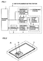
- Fig. 1 is a block diagram showing a basic structure of a non-contact IC card which can operate by receiving power from an interrogator.
- a resonance frequency of a resonance circuit 1 can be switched when a switch circuit in resonance circuit 1 is switched by a driving portion 5.
- Driving portion 5 sequentially switches the resonance frequency of resonance circuit 1.
- a reference voltage generating portion 6 receives an output voltage of resonance circuit 1 for converting it to a direct current voltage. It is noted that, although a magnitude of the converted direct current voltage changes by switching the resonance frequency, reference voltage generating portion 6 generates a prescribed reference voltage regardless of the change.
- An output value measuring portion 7 measures an output value of resonance circuit 1 at each resonance frequency using the reference voltage as a reference.
- the measured output value is stored in an output value storing portion 8 corresponding to each resonance frequency (that is, each switching manner).
- a manner determining portion 9 selects the largest one of output values stored in output value storing portion 8, and determines a corresponding switching manner as a preferred switching manner (a suitable switching manner).
- a suitable switching manner for the resonance frequency which allows the most efficient power supply is obtained.
- the suitable switching manner is stored in a switching manner storing portion 4.
- driving portion 5 drives the switch circuit in resonance circuit 1 in accordance with the suitable switching manner stored in switching manner storing portion 4, and determines the resonance frequency of resonance circuit 1.
- the resonance frequency needs not be adjusted every time when the non-contact IC card is operated. It is noted that switching manner storing portion 4 can hold a content even when power is not supplied.
- Fig. 2 is an illustration showing an internal structure of a non-contact IC card according to a first embodiment of the present invention.
- a non-contact IC card 10 includes an antenna 11, a plurality of condensers C and an IC chip 12 in a card like base material, which is shown with a chain-dotted line.
- Fig. 3 is a circuit block diagram showing a structure of non-contact IC card 10. Parts of the structure of IC card 10 excluding antenna 11 and condensers C1, C2, ⁇ , Cn are structured as an IC chip 12.
- a rectifying circuit 14 rectifies a received high-frequency carrier for applying it to a regulator 15. Regulator 15 stabilizes and supplies it for each portion as a power supply voltage VCC.
- a demodulating circuit 16 detects and demodulates the modulated high-frequency carrier for reproduction of data. The data is applied to CPU 17 for a prescribed process.
- Data is transmitted to an interrogator 50 by turning on/off a transistor for modulation MQ by CPU 17 for connecting/disconnecting a resistance element RM and a rectifying circuit 14 when interrogator 50 is outputting an unmodulated high-frequency carrier.
- an amplitude of the carrier is changed by changing an impedance for the side of interrogator 50, so that data is restored in interrogator 50.
- an operation program of CPU 17 is stored in a non-volatile memory 18.
- a resonance circuit 13 includes antenna 11, condensers C1, C2, ⁇ , Cn and transistors SQ1, SQ2, ⁇ , SQn which are switching means.
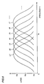
- a capacitance of condenser Cn/2 is designed such that a resonance frequency fn/2 of resonance circuit 13 formed of condenser Cn/2 and antenna 11 matches a frequency of a high-frequency carrier transmitted from interrogator 50.
- the capacitances of the other condensers are set such that the resonance frequencies thereof are slightly different starting from resonance frequency fn/2.
- IC card 10 is structured such that resonance frequency f1 when condenser C1 is connected is the lowest, resonance frequency fn when condenser Cn is connected is the highest, and differences between resonance frequencies of two adjacent condensers are equal.
- An output from regulator 15 is applied to a reference voltage generating circuit 19 which is a reference voltage generating means and an output value measuring circuit 20 which is an output value measuring means.
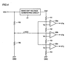
- Reference voltage generating circuit 19 and output value measuring circuit 20 are shown in Fig. 4 in greater detail.
- a band gap voltage generating circuit 21 is used as reference voltage generating circuit 19.
- Band gap voltage generating circuit 21 maintains its output voltage at a prescribed level even when power supply voltage VCC applied from regulator 15 changes. Thus, the output voltage is used as a reference voltage Vref.
- Reference voltage Vref is divided by resistance elements R1 to R4 for obtaining threshold voltages Va, Vb and Vc, and an output voltage of regulator 15 is divided by resistance elements R5 and R6.
- a program for automatically adjusting a resonance frequency is also stored in non-volatile memory 18 in addition to a program for communication.
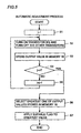
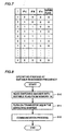
- a flow chart of the program for automatic adjustment is shown in Fig. 5.
- a process of automatically adjusting the resonance frequency will now be described with reference to the flow chart in Fig. 5 and the circuit block diagram in Fig. 3.
- CPU 17 stores outputs ⁇ A to ⁇ C from comparators 22a to 22c in non-volatile memory 18 such that they corresponds to switching manner j (a step S3) as shown in Fig. 7.
- a portion of non-volatile memory 18 shown in Fig. 7 corresponds to an output value storing means and a switching manner storing means.
- step S6 the largest one of the stored output values is selected.
- the largest output value is when switching manner j-4, 5 and 6.
- step S6 corresponds to a manner determining means in the present embodiment.
- step S10 switching manner j is obtained to which the suitable flag is applied from non-volatile memory 18 in a step S10. Then, transistor SQj designated by switching manner j is turned on (a step S11). Thus, power is supplied by the high-frequency carrier in the most efficient state from interrogator 50. Subsequently, a prescribed communication process is performed (a step S12). As described above, steps S10 and S11 correspond to the driving means in the present embodiment.
- the resonance frequency of resonance circuit 13 is automatically adjusted such that the power supply from interrogator 50 is maximum. Therefore, deviation of the resonance frequency of resonance circuit 13 caused by variation in authorized parts or the like can readily be adjusted during manufacture. In addition, once the adjustment is made, the suitable resonance frequency is achieved simply by performing an operation shown in Fig. 8, whereby decrease in operation speed is prevented.
- every switching manner is examined in order to achieve the suitable switching manner in the present embodiment.
- examination of the subsequent switching manners may be eliminated when the output value exceeding the prescribed threshold value is obtained, and the switching manner for the output value exceeding the threshold value is determined as the suitable switching manner.
- automatic adjustment is rapidly performed.
- IC chip 12 corresponds to a portion other than antenna 11 and condenser C as shown in Fig. 2.
- condenser C may be integrated with the IC chip.
- the number of contact terminals of the IC chip can be reduced in this way.
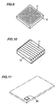
- antenna 11 may be provided on an upper surface of IC chip 12 by printing. Further, as shown in Fig. 10, antenna 11 may be wound around IC chip 12.
- antenna 11 is formed of an aluminum interconnection Layer in IC chip, so that the entire portion thereof is in IC chip 23. In these cases, the size of antenna 11 cannot be increased, thereby possibly decreasing efficiency. Therefore, it is particularly preferable to enable efficient power supply using the method of automatic adjustment according to the present invention.
- the non-contact IC card for performing power supply and data communication with the same carrier has been described in the first embodiment.
- a non-contact IC card for performing power supply and data communication with different carriers at different frequencies will be described.
- power is supplied from an interrogator by an unmodulated carrier f0, and data communication with the interrogator is performed by a carrier fL.
- a resonance circuit 26 for data communication includes an antenna 25 and a condenser C1.
- a demodulating circuit 16 demodulates data from the modulated carrier and applies it to CPU 17.
- CPU 17 turns on/off a transistor for modulation MQ to connect or disconnect a resistance element RM and resonance circuit 26 when the interrogator is outputting an unmodulated carrier fL.
- an amplitude of carrier fL is changed by changing an impedance for the interrogator, so that data is restored in the interrogator.
- Resonance circuit 13 for which power is supplied includes an antenna 11, condensers C1 to Cn and transistors SQ1 to SQn.
- the second embodiment is the same as the first embodiment in that CPU 17 determines a suitable switching manner for transistors SQ1 to SQn in accordance with an output VCC from a regulator 15 for storing it in non-volatile memory 18.
- Fig. 13 is a circuit block diagram showing a structure of a non-contact IC card according to a third embodiment of the present invention.
- the present embodiment is structured such that a resonance frequency is automatically adjusted not only in resonance circuit 13 for power supply but also in resonance circuit 32 for data communication.
- one of condensers TC1 to TCn is selected by transistors TQ1 to TQn and connected in parallel to antenna 31.
- an output value measuring circuit 34 determines a suitable switching manner by comparing an output from demodulating circuit 16 with a reference voltage generated in a reference voltage generating circuit 33. It is noted that the structures of reference voltage generating circuit 33 and output value measuring circuit 34 are similar to those of reference voltage generating circuit 19 and output value measuring circuit 20.
- the resonance frequency for data communication can also be automatically adjusted.
- a modulating circuit (a circuit corresponding to transistor MQ and resistance element RM in Fig. 12) for data communication with the interrogator is not separately provided. This is because an impedance for the interrogator is changed by switching between the suitable switching manner and the other switching manner in accordance with data under control of CPU 17.
- one of condensers C1 to Cn (TC1 to TCn) is connected to antenna 11 (25, 31).
- a switching manner which allows a plurality of condensers to be simultaneously connected to an antenna may be used. In this way, a number of switching manners are ensured with a small number of condensers.
- FIG. 14 Another exemplary structures of the resonance circuit allowing adjustment of a resonance frequency are shown in Figs. 14 to 16.
- the resonance circuit shown in Fig. 14 switches an effective inductance of an antenna 11 (25, 31) by short-circuiting a part of antenna 11 (25, 31) by a transistor SQ1 (TQ1) or SQ2 (TQ2).
- a resonance circuit shown in Fig. 15 allows one, two or three of condensers C1, C2 and C3 which are connected in series to be connected in parallel to antenna 11 (25, 31) by turning on or off transistor SQ1 (TQ1) or SQ2 (TQ2).
- a structure of the resonance circuit may be determined in consideration of how easy each element is formed, the number of connecting terminals required for an IC chip or the like.
- CPU 17 reads the suitable switching manner to which the suitable flag is applied from non-volatile memory 18 and, in accordance therewith, turns on one of transistors SQ1 to SQn when the non-contact IC card is in use.
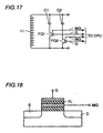
- a memory device for the suitable flag and the transistor may be shared by non-volatile memories FQ1, FQ2, ⁇ having a ferroelectric layer FL.
- Fig. 18 is a cross sectional view showing a structure of a non-volatile memory FQ.
- Non-volatile memory FQ can change a polarization direction of ferroelectric layer FL in accordance with a direction of a voltage applied between a gate G and a memory gate MG.
- a region between a source S and a drain D is turned on/off.
- CPU 17 polarizes ferroelectric layer FL of non-volatile memory FQ to be turned on in the suitable switching manner in an on direction.
- non-volatile memory FQ is automatically turned on, so that a condenser is selected such that a suitable resonance frequency is ensured without performing processes of steps S10 and S11 in Fig. 8 by CPU 17 during actual use.
- operation speed is increased.
- the resonance frequency is automatically adjusted during manufacture.
- the automatic adjustment may be performed once in a prescribed period of time for correcting change in the resonance frequency due to secular change or change in ambient temperature.
- automatic adjustment may be performed when a prescribed day arrives, when a prescribed period of time is elapsed after a previous adjustment, or when the device is used for a prescribed number of times.
- measurement of the day and the number of usage may be performed on the side of the interrogator or the IC card. It may also be performed by both of the interrogator and the IC card.
- pulse amplification modulation is performed for the carrier for data communication.
- the present invention can be applied to any method of modulation such as pulse frequency modulation, pulse phase modulation, analog amplitude modulation, analog frequency modulation and analog phase modulation.
- the present invention has been described as being applied to the non-contact IC card in the first to third embodiments, it is not limited to this and may be applied to an instrument performing a process other than communication as long as it externally receives power supply by a carrier.
- a responder is embodied in the form of the non-contact IC card in the first to third embodiments, the configuration of the responder is not limited to a card, and the responder may assume any configuration including a box, notebook or any other configuration.
- an expression "communication through electromagnetic wave” in the present invention indicates a radio communication utilizing an electromagnetic function, and is a concept including communication through electromagnetic coupling in addition to communication utilizing a radiowave.
- switching means corresponds to a means capable of switching a connection state of a circuit and a constant, regardless of a mechanical or electrical structure. It does not only digitally switches between on and off but also successively switches a constant such as a resistance value in an analog manner.
- transistors SQ1 to SQn in Figs. 3 and 12 and transistors TQ1 to TQn correspond to this.
- transistor is a device which controllably turns on/off by a control voltage (current) applied to a gate, base or the like.
- the term "antenna” is an element having an inductance component necessary for receiving a desired electromagnetic wave regardless of its shape, formation method or the like.
- the antenna may be a wiring wound in a form of a coil as shown in Figs. 2 and 10, printed on a surface of IC chip 12 as shown in Fig. 9, or formed as an aluminum interconnection layer in IC chip 23 as shown in Fig. 11.
- condenser is an element having a capacitance necessary for forming a transmitting circuit with the antenna regardless of its shape, formation method or the like.
- condensers C1 to Cn in Fig. 3 and condensers TC1 to TCn in Fig. 13 correspond to this.
- a floating capacitance of the antenna may be used as a condenser.
Landscapes
- Engineering & Computer Science (AREA)
- Computer Hardware Design (AREA)
- Microelectronics & Electronic Packaging (AREA)
- Physics & Mathematics (AREA)
- General Physics & Mathematics (AREA)
- Theoretical Computer Science (AREA)
- Computer Networks & Wireless Communication (AREA)
- Near-Field Transmission Systems (AREA)
- Credit Cards Or The Like (AREA)
Abstract
Description
Claims (23)
- A responder for communicating with an interrogator by an electromagnetic wave in a non-contact IC card communication system; comprising:a resonance circuit (1, 13, 26, 32) including an antenna (11, 25, 31) receiving the electromagnetic wave from said interrogator and switching means (SQ, TQ) and capable of switching a resonance frequency by said switching means (SQ, TQ); andswitching manner setting means (2) sequentially switching the resonance frequency of said resonance circuit (1, 13, 26, 32) by using said switching means (SQ, TQ) and detecting an output level of said resonance circuit (1, 13, 26, 32) in each switching manner and, in accordance with a detection result, setting a switching manner of said switching means (SQ, TQ) such that a desired output level is obtained.
- The responder in the non-contact IC card communication system according to claim 1, wherein said switching manner setting means (2) includes:determining means (3) sequentially switching the switching means (SQ, TQ) of said resonance circuit (1, 13, 26, 32) and detecting an output voltage or output current of said resonance circuit (1, 13, 26, 32) in each switching manner and, in accordance with a detection result, obtaining a suitable switching manner of said switching means (SQ, TQ) producing a desired output voltage or output current; andswitching manner storing means (4, 18) storing the suitable switching manner obtained by said determining means (3).
- The responder in the non-contact IC card communication system according to claim 2, whereinsaid responder is formed to receive the electromagnetic wave from the interrogator as a power source, and said determining means (3) includes:reference voltage generating means (6, 19, 33) receiving the output voltage of said resonance circuit (1, 13, 26, 32) for generating a prescribed reference voltage regardless of variation in the output voltage;output value measuring means (7, 20, 34) measuring a magnitude of the output voltage of said resonance circuit (1, 13, 26, 32) in each switching manner by using the reference voltage generated in said reference voltage generating means (6, 19, 33) as a reference and outputting each measurement result as an output value; andmanner determining means (9, 17) determining said suitable switching manner in accordance with the output value output from said output value measuring means (7, 20, 34).
- The responder in the non-contact IC card communication system according to claim 3, wherein said determining means (3) further includes output value storing means (8, 18) storing each output value output from said output value measuring means (7, 20, 34) corresponding to each switching manner of said switching means (SQ, TQ), andsaid manner determining means (9, 17) determines said suitable switching manner in accordance with said output value read from said output value storing means (8, 18).
- The responder in the non-contact IC card communication system according to claim 3, wherein said manner determining means (9, 17) determines a switching manner corresponding to a largest output value as said suitable switching manner.
- The responder in the non-contact IC card communication system according to claim 3, wherein said manner determining means (9, 17) receives the output value every time said switching manner is sequentially switched and, in response to a fact that an output value exceeding a prescribed threshold value is applied, determines the switching manner corresponding to the output value as said suitable switching manner.
- The responder in the non-contact IC card communication system according to one of claims 1 to 6, wherein said resonance circuit (1, 13, 26, 32) is further provided with a variable capacitance circuit (C, SQ, TQ) connected in parallel to said antenna (11, 25, 31) and including a plurality of condensers (C) and said switching means (SQ, TQ), anda capacitance of said variable capacitance circuit (C, SQ, TQ) can be switched by said switching means (SQ, TQ).
- The responder in the non-contact IC card communication system according to one of claims 1 to 6, wherein said resonance circuit (1, 13, 26, 32) further includes a condenser (C) connected in parallel to said antenna (11, 25, 31), andan inductance of said antenna (11, 25, 31) can be switched by said switching means (SQ, TQ).
- The responder in the non-contact IC card communication system according to one of claims 2 to 6, wherein said switching means (SQ, TQ) includes a plurality of transistors (SQ, TQ), andsaid switching manner storing means (4, 18) stores which one of said plurality of transistors (SQ, TQ) is rendered conductive.
- The responder in the non-contact IC card communication system according to one of claims 1 to 6, wherein said resonance circuit (1, 13, 26, 32) is used at least for supplying operation power of said responder.
- The responder in the non-contact IC card communication system according to one of claims 1 to 6, wherein said resonance circuit (1, 13, 26, 32) is used at least for data communication with said interrogator.
- The non-contact IC card communication system according to one of claims 1 to 6, wherein said determining means (3) determines said suitable switching manner during manufacture of said responder.
- The responder in the non-contact IC card communication system according to one of claims 1 to 6, wherein said determining means (3) determines said suitable switching manner once in a prescribed period of time.
- The responder in the non-contact IC card communication system according to claim 13, wherein said prescribed period of time is between a previous determination time and a time when a prescribed amount of time has elapsed.
- The responder in the non-contact IC card communication system according to claim 13, wherein said prescribed period of time is between a previous determination date and a time when said responder is used a prescribed number of times.
- The responder in the non-contact IC card communication system according to one of claims 1 to 6, wherein said resonance circuit (1, 13, 26, 32) and said switching manner setting means (2) are formed as an integrated circuit chip.
- An integrated circuit chip used in a device with no self-contained power supply receiving an electromagnetic wave from an interrogator and capable of operating using the electromagnetic wave as a power source, comprising:a resonance circuit (1, 13, 26, 32) including an antenna (11, 25, 31) receiving the electromagnetic wave from said interrogator and switching means (SQ, TQ) and capable of switching a resonance frequency by said switching means (SQ, TQ);determining means (3) sequentially switching said switching means (SQ, TQ) of said resonance circuit (1, 13, 26, 32) and detecting an output level of said resonance circuit (1, 13, 26, 32) in each switching manner and, in accordance with a detection result, obtaining a suitable switching manner of said switching means (SQ, TQ) producing a desired output level; andswitching manner storing means storing the suitable switching manner obtained by said determining means (3).
- An integrated circuit chip used in a device with no self-contained power supply receiving an electromagnetic wave from an interrogator and capable of operating using the electromagnetic wave as a power source, comprising:a first connection terminal for connection to an external resonance circuit (1, 13, 26, 32);a second connection terminal for applying a signal to switching means (SQ, TQ) switching a resonance frequency of said resonance circuit (1, 13, 26, 32);determining means (3) sequentially switching said switching means (SQ, TQ) and detecting an output level of said resonance circuit (1, 13, 26, 32) in each switching manner and, in accordance with detection result, obtaining a suitable switching manner of said switching means (SQ, TQ) producing a desired output level; andswitching manner storing means (4, 18) storing the suitable switching manner obtained by said determining means (3).
- An integrated circuit chip used in a device with no self-contained power supply receiving an electromagnetic wave from an interrogator and capable of operating using the electromagnetic wave as a power source, comprising:a plurality of connection terminals to which antennas (11, 25, 31) with different inductances are connected;a condenser (C) forming a resonance circuit (1, 13, 26, 32) with said antenna (11, 25, 31);switching means (SQ, TQ) selectively connecting said condenser (C) to one of said plurality of connection terminals;determining means (3) sequentially switching said switching means (SQ, TQ) and detecting an output level of said resonance circuit (1, 13, 26, 32) in each switching manner and, in accordance with a detection result, obtaining a suitable switching manner of said switching means (SQ, TQ) producing a prescribed output level; andswitching manner storing means (4, 18) storing the suitable switching manner obtained by said determining means (3).
- An integrated circuit chip used in a device with no self-contained power supply receiving an electromagnetic wave from an interrogator and capable of operating using the electromagnetic wave as a power source, comprising:a connection terminal for connection to an external antenna (11, 25, 31);a plurality of condensers (C) with different capacitances forming resonance circuit (1, 13, 26, 32) with said antenna (11, 25, 31);switching means (SQ, TQ) selectively connecting one of said plurality of condensers (C) to said connection terminal;determining means (3) sequentially switching said switching means (SQ, TQ) and detecting an output level of said resonance circuit (1, 13, 26, 32) in each switching manner and, in accordance with a determination result, obtaining a suitable switching manner of said switching means (SQ, TQ) producing a desired output level; andswitching manner storing means (4, 18) storing the suitable switching manner obtained by said determining means (3).
- A non-contact IC card receiving an electromagnetic wave from an interrogator for communication with said interrogator by using the electromagnetic wave as a power source, comprising:a resonance circuit (1, 13, 26, 32) including an antenna (11, 25, 31) receiving the electromagnetic wave from said interrogator, a condenser (C) and a plurality of transistors (SQ, TQ), and capable of switching at least one of an inductance of said antenna (11, 25, 31) and a capacitance of said condenser (C) depending on which one of said plurality of transistors (SQ, TQ) is rendered conductive;reference voltage generating means (6, 19, 33) receiving an output voltage of said resonance circuit (1, 13, 26, 32) for generating a prescribed reference voltage regardless of variation in the output voltage;sequentially driving means (5) sequentially rendering each of said plurality of transistors (SQ, TQ) of said resonance circuit (1, 13, 26, 32) conductive;output value measuring means (7, 20, 34) measuring a magnitude of the output voltage of said resonance circuit (1, 13, 26, 32) in each switching manner of said plurality of transistors (SQ, TQ) by said sequentially driving means (5) using a reference voltage generated in said reference voltage generating means (6, 19, 33) as a reference for outputting each measurement value as an output value;output value storing means (8, 18) storing each of said output values output from said output value measuring means (7, 20, 34) corresponding to each switching manner;manner determining means (9, 17) determining a switching manner corresponding to a largest one of said output values in each switching manner stored in said output value storing means (8, 18) as a suitable switching manner;switching manner storing means (4, 18) storing said suitable switching manner obtained by said manner determining means (9, 17); anddriving means (5) driving said plurality of transistors (SQ, TQ) of said resonance circuit (1, 13, 26, 32) in accordance with said suitable switching manner read from said switching manner storing means (4, 18).
- A device with no self-contained power supply receiving an electromagnetic wave through a resonance circuit (1, 13, 26, 32) as a power source; whereina resonance frequency of said resonance circuit (1, 13, 26, 32) in which said resonance frequency can be changed by a switching signal is sequentially changed,a reference voltage generating source (6, 19, 33) is provided receiving a voltage generated by said resonance circuit (1, 13, 26, 32) in accordance with the received electromagnetic wave for generating a prescribed reference voltage regardless of variation in the voltage; andeach output voltage of said resonance circuit (1, 13, 26, 32) corresponding to each resonance frequency sequentially changed is measured by using said reference voltage as a reference, and the switching signal is applied to said resonance circuit (1, 13, 26, 32) to provide the resonance frequency producing a largest output value for obtaining a largest amount of power.
- A method of automatically adjusting a device with no self-contained power supply receiving an electromagnetic wave through resonance circuit (1, 13, 26, 32) as a power source, comprising the steps of:sequentially changing a resonance frequency of said resonance circuit (1, 13, 26, 32) capable of changing the resonance frequency by a switching signal;receiving a voltage generated by said resonance circuit (1, 13, 26, 32) in accordance with the received electromagnetic wave and determining an output from a reference voltage generating source (6, 19, 33) generating a prescribed reference voltage regardless of variation in the voltage as a reference voltage; andmeasuring each output voltage from said resonance circuit (1, 13, 26, 32) corresponding to each resonance frequency sequentially changed using said reference voltage as a reference and applying a switching signal to said resonance circuit (1, 13, 26, 32) to produce the resonance frequency allowing a largest output voltage for obtaining a largest amount of power.
Applications Claiming Priority (3)
| Application Number | Priority Date | Filing Date | Title |
|---|---|---|---|
| JP8349700A JPH10187916A (en) | 1996-12-27 | 1996-12-27 | Responder for contactless ic card communication system |
| JP34970096 | 1996-12-27 | ||
| PCT/JP1997/004505 WO1998029828A1 (en) | 1996-12-27 | 1997-12-08 | Responder, integrated circuit chip, noncontact ic card, and self power needless type device in noncontact ic card communication system, and automatic adjustment method for self power needless type device |
Publications (3)
| Publication Number | Publication Date |
|---|---|
| EP1022677A1 true EP1022677A1 (en) | 2000-07-26 |
| EP1022677A4 EP1022677A4 (en) | 2000-11-02 |
| EP1022677B1 EP1022677B1 (en) | 2002-10-30 |
Family
ID=18405520
Family Applications (1)
| Application Number | Title | Priority Date | Filing Date |
|---|---|---|---|
| EP97946157A Expired - Lifetime EP1022677B1 (en) | 1996-12-27 | 1997-12-08 | Non-contact ic card without self contained power supply |
Country Status (8)
| Country | Link |
|---|---|
| US (1) | US6624743B1 (en) |
| EP (1) | EP1022677B1 (en) |
| JP (1) | JPH10187916A (en) |
| KR (1) | KR100341629B1 (en) |
| AU (1) | AU748393B2 (en) |
| CA (1) | CA2274553A1 (en) |
| DE (1) | DE69716783T2 (en) |
| WO (1) | WO1998029828A1 (en) |
Cited By (14)
| Publication number | Priority date | Publication date | Assignee | Title |
|---|---|---|---|---|
| EP1369816A1 (en) * | 2002-06-07 | 2003-12-10 | Sony Corporation | Tuning capacitors for IC module in wireless IC card |
| EP1061663A4 (en) * | 1998-11-11 | 2004-06-30 | Mitsubishi Materials Corp | Identification method for overlapped tags |
| EP1538557A3 (en) * | 2003-12-05 | 2009-04-29 | STMicroelectronics S.A. | Resistive and capacitive modulation in an electromagnetic transponder |
| EP2068272A1 (en) | 2007-12-07 | 2009-06-10 | Sony Ericsson Mobile Communications Japan, Inc. | Non-contact wireless communication apparatus, method of adjusting resonance frequency of non-contact wireless communication antenna, and mobile terminal apparatus |
| WO2009140220A1 (en) * | 2008-05-13 | 2009-11-19 | Qualcomm Incorporated | Method and apparatus for adaptive tuning of wireless power transfer |
| EP1895450A3 (en) * | 2006-08-31 | 2010-01-06 | Semiconductor Energy Laboratory Co., Ltd. | Semiconductor device and power receiving device |
| US8552921B2 (en) | 2007-02-09 | 2013-10-08 | Semiconductor Energy Laboratory Co., Ltd. | Semiconductor device |
| US8854224B2 (en) | 2009-02-10 | 2014-10-07 | Qualcomm Incorporated | Conveying device information relating to wireless charging |
| US8878393B2 (en) | 2008-05-13 | 2014-11-04 | Qualcomm Incorporated | Wireless power transfer for vehicles |
| US9312924B2 (en) | 2009-02-10 | 2016-04-12 | Qualcomm Incorporated | Systems and methods relating to multi-dimensional wireless charging |
| US9479225B2 (en) | 2010-05-13 | 2016-10-25 | Qualcomm Incorporated | Resonance detection and control within a wireless power system |
| WO2017008878A1 (en) * | 2015-07-16 | 2017-01-19 | Sew-Eurodrive Gmbh & Co. Kg | Assembly for the inductive transfer of electrical energy from a stationary primary conductor to a device that can move relative to same, and method for operating the assembly |
| US9583953B2 (en) | 2009-02-10 | 2017-02-28 | Qualcomm Incorporated | Wireless power transfer for portable enclosures |
| EP4661302A4 (en) * | 2023-02-01 | 2026-04-22 | Nuvoton Technology Corp Japan | CONTACTLESS COMMUNICATION DEVICE, CONTROL METHOD AND PROGRAM |
Families Citing this family (45)
| Publication number | Priority date | Publication date | Assignee | Title |
|---|---|---|---|---|
| JPH10187916A (en) | 1996-12-27 | 1998-07-21 | Rohm Co Ltd | Responder for contactless ic card communication system |
| FR2781074B1 (en) * | 1998-07-08 | 2006-04-28 | Commissariat Energie Atomique | ANALOG INTERFACE FOR AUTONOMOUS INFORMATION EXCHANGE CIRCUIT |
| US6850991B1 (en) | 1998-12-22 | 2005-02-01 | Citibank, N.A. | Systems and methods for distributing information to a diverse plurality of devices |
| FR2801745B1 (en) * | 1999-11-30 | 2007-05-25 | St Microelectronics Sa | ELECTROMAGNETIC TRANSPONDER WITH DISCONNECTION IN FREQUENCY |
| JP3488166B2 (en) * | 2000-02-24 | 2004-01-19 | 日本電信電話株式会社 | Contactless IC card system, its reader / writer and contactless IC card |
| CN1185599C (en) * | 2000-08-15 | 2005-01-19 | 欧姆龙株式会社 | Noncontact communication medium and noncontact communication system |
| JP3650317B2 (en) * | 2000-08-23 | 2005-05-18 | 日本電信電話株式会社 | Electromagnetic field receiver |
| GB0210886D0 (en) * | 2002-05-13 | 2002-06-19 | Zap Wireless Technologies Ltd | Improvements relating to contact-less power transfer |
| JP4614961B2 (en) * | 2003-05-23 | 2011-01-19 | オークランド ユニサービシズ リミテッド | Method and apparatus for controlling an inductively coupled power transfer system |
| JP4536496B2 (en) * | 2003-12-19 | 2010-09-01 | 株式会社半導体エネルギー研究所 | Semiconductor device and driving method of semiconductor device |
| US7471188B2 (en) | 2003-12-19 | 2008-12-30 | Semiconductor Energy Laboratory Co., Ltd. | Semiconductor device and driving method thereof |
| US7132946B2 (en) * | 2004-04-08 | 2006-11-07 | 3M Innovative Properties Company | Variable frequency radio frequency identification (RFID) tags |
| US7504935B2 (en) * | 2004-04-19 | 2009-03-17 | Siemens Aktiengesellschaft | Transponder |
| JPWO2006008816A1 (en) * | 2004-07-22 | 2008-05-01 | 三菱電機株式会社 | Non-contact type terminal and reader / writer device |
| JP2006197277A (en) * | 2005-01-14 | 2006-07-27 | Hitachi Ltd | Wireless tag and wireless communication system |
| DE102006017992A1 (en) * | 2006-04-07 | 2007-10-18 | Balluff Gmbh | Data carrier / transmitting device and method for producing a data carrier / transmitting device |
| JP4382063B2 (en) | 2006-06-07 | 2009-12-09 | フェリカネットワークス株式会社 | Information processing terminal and reception voltage control method |
| JP2007334507A (en) * | 2006-06-13 | 2007-12-27 | Felica Networks Inc | Integrated circuit, non-contact type ic card, reader/writer, radio communication method and computer program |
| US8208665B2 (en) | 2007-01-10 | 2012-06-26 | Siemens Audiologische Technik Gmbh | Hearing apparatus with automatic self trimming and corresponding method |
| DE102007001538B4 (en) * | 2007-01-10 | 2015-02-12 | Siemens Audiologische Technik Gmbh | Hearing device with automatic self-trim and corresponding method |
| JP4488040B2 (en) | 2007-07-26 | 2010-06-23 | Tdk株式会社 | Radio communication transmitter / receiver, RFID system, and radio communication transmitter / receiver reception method |
| KR20120102173A (en) * | 2007-09-13 | 2012-09-17 | 퀄컴 인코포레이티드 | Antennas for wireless power applications |
| US7971794B2 (en) * | 2008-02-07 | 2011-07-05 | Infineon Technologies Ag | Actively regulated modulation index for contactless IC devices |
| US8855554B2 (en) * | 2008-03-05 | 2014-10-07 | Qualcomm Incorporated | Packaging and details of a wireless power device |
| CN102017361B (en) | 2008-04-21 | 2016-02-24 | 高通股份有限公司 | wireless power transfer system and method |
| JP2009268181A (en) * | 2008-04-22 | 2009-11-12 | Olympus Corp | Energy supply apparatus |
| CN104077622B (en) | 2008-05-26 | 2016-07-06 | 株式会社村田制作所 | The authenticating method of wireless IC device system and Wireless IC device |
| WO2010005324A1 (en) * | 2008-07-07 | 2010-01-14 | Powerbyproxi Limited | A contactless power receiver and method of operation |
| JP5252550B2 (en) * | 2008-09-24 | 2013-07-31 | 日立マクセル株式会社 | Non-contact IC card |
| JP5185789B2 (en) * | 2008-11-26 | 2013-04-17 | 京セラ株式会社 | Wireless communication device |
| US8497658B2 (en) | 2009-01-22 | 2013-07-30 | Qualcomm Incorporated | Adaptive power control for wireless charging of devices |
| JP2010252468A (en) * | 2009-04-14 | 2010-11-04 | Sony Corp | Power transmission device and method, power reception device and method, and power transmission system |
| JP5278197B2 (en) | 2009-06-29 | 2013-09-04 | ソニー株式会社 | Non-contact communication device and non-contact communication method |
| JP5293586B2 (en) * | 2009-12-15 | 2013-09-18 | 富士通株式会社 | Non-contact IC card system |
| JP5041610B2 (en) * | 2010-11-01 | 2012-10-03 | 則雄 宮内 | Wireless charging apparatus and wireless charging method thereof |
| US8659015B2 (en) | 2011-03-04 | 2014-02-25 | Semiconductor Energy Laboratory Co., Ltd. | Semiconductor device |
| NZ593946A (en) * | 2011-07-07 | 2014-05-30 | Powerbyproxi Ltd | An inductively coupled power transfer receiver |
| JP2013126326A (en) * | 2011-12-15 | 2013-06-24 | Toyota Motor Corp | Non-contact power receiving apparatus and vehicle equipped with the same, non-contact power transmission apparatus, and non-contact power feeding system |
| JP2014023328A (en) * | 2012-07-20 | 2014-02-03 | Heads Corp | Non-contact power-feeding device |
| WO2015140917A1 (en) * | 2014-03-18 | 2015-09-24 | 三菱電機エンジニアリング株式会社 | Resonance power transmission apparatus, transmission-side power transmission apparatus, and reception-side power transmission apparatus |
| CN105528633A (en) * | 2015-07-10 | 2016-04-27 | 北京中电华大电子设计有限责任公司 | Frequency adaptive adjusting device and method for non-contact chip |
| JP6808369B2 (en) * | 2016-06-20 | 2021-01-06 | キヤノン株式会社 | Power receiving device, its control method and program |
| CN107809263B (en) | 2016-09-08 | 2021-04-27 | 三星电子株式会社 | Near Field Communication Device |
| KR102570787B1 (en) | 2016-10-27 | 2023-08-24 | 삼성전자주식회사 | Recognition device for NFC tag and system including the same |
| EP3779794B1 (en) * | 2018-04-09 | 2023-09-06 | Sony Semiconductor Solutions Corporation | Non-contact communication medium, driving method thereof, and recording medium cartridge |
Family Cites Families (14)
| Publication number | Priority date | Publication date | Assignee | Title |
|---|---|---|---|---|
| JPS601787B2 (en) | 1980-06-06 | 1985-01-17 | 日本電気株式会社 | Wireless transmission method |
| EP0640254B1 (en) | 1992-05-10 | 2001-08-01 | Auckland Uniservices Limited | A non-contact power distribution system |
| US5446447A (en) * | 1994-02-16 | 1995-08-29 | Motorola, Inc. | RF tagging system including RF tags with variable frequency resonant circuits |
| JPH087059A (en) | 1994-06-21 | 1996-01-12 | Sony Chem Corp | Contactless information card |
| US5621396A (en) * | 1994-06-30 | 1997-04-15 | Texas Instruments Incorporated | Method and apparatus with adaptive transponder plucking |
| US5621767A (en) * | 1994-09-30 | 1997-04-15 | Hughes Electronics | Method and device for locking on a carrier signal by dividing frequency band into segments for segment signal quality determination and selecting better signal quality segment |
| JPH0962816A (en) * | 1994-10-06 | 1997-03-07 | Mitsubishi Electric Corp | Contactless IC card and contactless IC card system including the same |
| US5953642A (en) | 1994-10-26 | 1999-09-14 | Siemens Aktiengesellschaft | System for contactless power and data transmission |
| DE4438287C1 (en) * | 1994-10-26 | 1996-05-09 | Siemens Ag | System for contactless energy and data transmission |
| DE4438286C2 (en) | 1994-10-26 | 2002-09-12 | Siemens Ag | System for contactless energy and data transmission |
| JPH08167012A (en) * | 1994-12-13 | 1996-06-25 | Toshiba Corp | Data storage medium |
| DE19614455A1 (en) * | 1996-04-12 | 1997-10-16 | Philips Patentverwaltung | Method for operating a system from a base station and a transponder coupled to it in a contactless manner, and a suitable system for this |
| JP3867251B2 (en) * | 1996-09-13 | 2007-01-10 | テミツク セミコンダクター ゲゼルシヤフト ミツト ベシユレンクテル ハフツング | Method for transmitting data in a radio frequency identification system |
| JPH10187916A (en) | 1996-12-27 | 1998-07-21 | Rohm Co Ltd | Responder for contactless ic card communication system |
-
1996
- 1996-12-27 JP JP8349700A patent/JPH10187916A/en active Pending
-
1997
- 1997-12-08 CA CA002274553A patent/CA2274553A1/en not_active Abandoned
- 1997-12-08 KR KR1019997005433A patent/KR100341629B1/en not_active Expired - Fee Related
- 1997-12-08 AU AU51391/98A patent/AU748393B2/en not_active Ceased
- 1997-12-08 US US09/319,253 patent/US6624743B1/en not_active Expired - Fee Related
- 1997-12-08 DE DE69716783T patent/DE69716783T2/en not_active Expired - Fee Related
- 1997-12-08 EP EP97946157A patent/EP1022677B1/en not_active Expired - Lifetime
- 1997-12-08 WO PCT/JP1997/004505 patent/WO1998029828A1/en not_active Ceased
Cited By (25)
| Publication number | Priority date | Publication date | Assignee | Title |
|---|---|---|---|---|
| EP1061663A4 (en) * | 1998-11-11 | 2004-06-30 | Mitsubishi Materials Corp | Identification method for overlapped tags |
| US6963028B2 (en) | 2002-06-07 | 2005-11-08 | Sony Corporation | IC module, and wireless information-storage medium and wireless information-transmitting/receiving apparatus including the IC wireless |
| US6974909B2 (en) | 2002-06-07 | 2005-12-13 | Sony Corporation | IC module, and wireless information-storage medium and wireless information-transmitting/receiving apparatus including the IC module |
| EP1369816A1 (en) * | 2002-06-07 | 2003-12-10 | Sony Corporation | Tuning capacitors for IC module in wireless IC card |
| EP1538557A3 (en) * | 2003-12-05 | 2009-04-29 | STMicroelectronics S.A. | Resistive and capacitive modulation in an electromagnetic transponder |
| US9022293B2 (en) | 2006-08-31 | 2015-05-05 | Semiconductor Energy Laboratory Co., Ltd. | Semiconductor device and power receiving device |
| EP1895450A3 (en) * | 2006-08-31 | 2010-01-06 | Semiconductor Energy Laboratory Co., Ltd. | Semiconductor device and power receiving device |
| US10256669B2 (en) | 2006-08-31 | 2019-04-09 | Semiconductor Energy Laboratory Co., Ltd. | Semiconductor device and power receiving device |
| US9531214B2 (en) | 2006-08-31 | 2016-12-27 | Semiconductor Energy Laboratory Co., Ltd. | Semiconductor device and power receiving device |
| US8552921B2 (en) | 2007-02-09 | 2013-10-08 | Semiconductor Energy Laboratory Co., Ltd. | Semiconductor device |
| EP2068272A1 (en) | 2007-12-07 | 2009-06-10 | Sony Ericsson Mobile Communications Japan, Inc. | Non-contact wireless communication apparatus, method of adjusting resonance frequency of non-contact wireless communication antenna, and mobile terminal apparatus |
| US8260200B2 (en) | 2007-12-07 | 2012-09-04 | Sony Mobile Communications Japan, Inc. | Non-contact wireless communication apparatus, method of adjusting resonance frequency of non-contact wireless communication antenna, and mobile terminal apparatus |
| WO2009140220A1 (en) * | 2008-05-13 | 2009-11-19 | Qualcomm Incorporated | Method and apparatus for adaptive tuning of wireless power transfer |
| US8892035B2 (en) | 2008-05-13 | 2014-11-18 | Qualcomm Incorporated | Repeaters for enhancement of wireless power transfer |
| US8878393B2 (en) | 2008-05-13 | 2014-11-04 | Qualcomm Incorporated | Wireless power transfer for vehicles |
| US9184632B2 (en) | 2008-05-13 | 2015-11-10 | Qualcomm Incorporated | Wireless power transfer for furnishings and building elements |
| US9954399B2 (en) | 2008-05-13 | 2018-04-24 | Qualcomm Incorporated | Reverse link signaling via receive antenna impedance modulation |
| US9991747B2 (en) | 2008-05-13 | 2018-06-05 | Qualcomm Incorporated | Signaling charging in wireless power environment |
| US8487478B2 (en) | 2008-05-13 | 2013-07-16 | Qualcomm Incorporated | Wireless power transfer for appliances and equipments |
| US9312924B2 (en) | 2009-02-10 | 2016-04-12 | Qualcomm Incorporated | Systems and methods relating to multi-dimensional wireless charging |
| US8854224B2 (en) | 2009-02-10 | 2014-10-07 | Qualcomm Incorporated | Conveying device information relating to wireless charging |
| US9583953B2 (en) | 2009-02-10 | 2017-02-28 | Qualcomm Incorporated | Wireless power transfer for portable enclosures |
| US9479225B2 (en) | 2010-05-13 | 2016-10-25 | Qualcomm Incorporated | Resonance detection and control within a wireless power system |
| WO2017008878A1 (en) * | 2015-07-16 | 2017-01-19 | Sew-Eurodrive Gmbh & Co. Kg | Assembly for the inductive transfer of electrical energy from a stationary primary conductor to a device that can move relative to same, and method for operating the assembly |
| EP4661302A4 (en) * | 2023-02-01 | 2026-04-22 | Nuvoton Technology Corp Japan | CONTACTLESS COMMUNICATION DEVICE, CONTROL METHOD AND PROGRAM |
Also Published As
| Publication number | Publication date |
|---|---|
| DE69716783T2 (en) | 2003-08-14 |
| KR20000057635A (en) | 2000-09-25 |
| EP1022677A4 (en) | 2000-11-02 |
| DE69716783D1 (en) | 2002-12-05 |
| AU748393B2 (en) | 2002-06-06 |
| KR100341629B1 (en) | 2002-06-22 |
| AU5139198A (en) | 1998-07-31 |
| EP1022677B1 (en) | 2002-10-30 |
| JPH10187916A (en) | 1998-07-21 |
| WO1998029828A1 (en) | 1998-07-09 |
| CA2274553A1 (en) | 1998-07-09 |
| US6624743B1 (en) | 2003-09-23 |
Similar Documents
| Publication | Publication Date | Title |
|---|---|---|
| EP1022677B1 (en) | Non-contact ic card without self contained power supply | |
| EP1014301B1 (en) | Response device in ic-card communication system | |
| JP3962099B2 (en) | High frequency tag and information exchange system using the same | |
| AU747890B2 (en) | Data communication equipment, data communication system, and data communication method | |
| US8335470B2 (en) | Communication apparatus and method for controlling the same | |
| US6650229B1 (en) | Electromagnetic transponder read terminal operating in very close coupling | |
| US6126077A (en) | Data processing apparatus and method and data transmitting/receiving apparatus and method | |
| US6848620B2 (en) | Semiconductor integrated circuit | |
| US8243863B2 (en) | Semiconductor device | |
| JP2009111483A (en) | Non-contact data carrier, reader / writer device, and non-contact data carrier system | |
| EP1538558A2 (en) | RFID with a resonant circuit | |
| JP2007193780A (en) | RFID tag and RFID system having the same | |
| JP5252550B2 (en) | Non-contact IC card | |
| JPH1125238A (en) | IC card | |
| CN1242092A (en) | Responder, integrated circuit chip. noncontact IC card, and self power needless type device in noncontact IC card communication system, and automatic adjustment method for self power needless device | |
| CN100353729C (en) | Transponder with two supply voltages | |
| CN100375116C (en) | Device for controlling impedance of antenna returning to electronic mark | |
| US11741333B2 (en) | Matching operating parameters in a smart card | |
| CN1179297C (en) | Data carrier with power input regulation | |
| JP2003323595A (en) | Non-contact IC card reader / writer device | |
| JP2007058381A (en) | Antenna circuit | |
| JP2000259788A (en) | Contactless IC card system and external read / write device for contactless IC card | |
| JP2002222399A (en) | Non-contact IC card |
Legal Events
| Date | Code | Title | Description |
|---|---|---|---|
| PUAI | Public reference made under article 153(3) epc to a published international application that has entered the european phase |
Free format text: ORIGINAL CODE: 0009012 |
|
| 17P | Request for examination filed |
Effective date: 19990629 |
|
| AK | Designated contracting states |
Kind code of ref document: A1 Designated state(s): DE FR GB NL |
|
| A4 | Supplementary search report drawn up and despatched |
Effective date: 20000915 |
|
| AK | Designated contracting states |
Kind code of ref document: A4 Designated state(s): DE FR GB NL |
|
| RIC1 | Information provided on ipc code assigned before grant |
Free format text: 7G 06K 19/00 A, 7G 06K 19/07 B |
|
| 17Q | First examination report despatched |
Effective date: 20001227 |
|
| RTI1 | Title (correction) |
Free format text: NON-CONTACT IC CARD WITHOUT SELF CONTAINED POWER SUPPLY |
|
| GRAG | Despatch of communication of intention to grant |
Free format text: ORIGINAL CODE: EPIDOS AGRA |
|
| GRAG | Despatch of communication of intention to grant |
Free format text: ORIGINAL CODE: EPIDOS AGRA |
|
| GRAH | Despatch of communication of intention to grant a patent |
Free format text: ORIGINAL CODE: EPIDOS IGRA |
|
| GRAH | Despatch of communication of intention to grant a patent |
Free format text: ORIGINAL CODE: EPIDOS IGRA |
|
| GRAA | (expected) grant |
Free format text: ORIGINAL CODE: 0009210 |
|
| RIN1 | Information on inventor provided before grant (corrected) |
Inventor name: YOSHIOKA, SATOSHI ROHM CO., LTD. Inventor name: CHIMURA, SHIGEMI ROHM CO., LTD. Inventor name: IKEFUJI, YOSHIHIRO ROHM CO., LTD. |
|
| RAP1 | Party data changed (applicant data changed or rights of an application transferred) |
Owner name: ROHM CO., LTD. |
|
| RIN1 | Information on inventor provided before grant (corrected) |
Inventor name: YOSHIOKA, SATOSHI ROHM CO., LTD. Inventor name: CHIMURA, SHIGEMI ROHM CO., LTD. Inventor name: IKEFUJI, YOSHIHIRO ROHM CO., LTD. |
|
| AK | Designated contracting states |
Kind code of ref document: B1 Designated state(s): DE FR GB NL |
|
| PG25 | Lapsed in a contracting state [announced via postgrant information from national office to epo] |
Ref country code: NL Free format text: LAPSE BECAUSE OF FAILURE TO SUBMIT A TRANSLATION OF THE DESCRIPTION OR TO PAY THE FEE WITHIN THE PRESCRIBED TIME-LIMIT Effective date: 20021030 |
|
| REG | Reference to a national code |
Ref country code: GB Ref legal event code: FG4D |
|
| REF | Corresponds to: |
Ref document number: 69716783 Country of ref document: DE Date of ref document: 20021205 |
|
| PG25 | Lapsed in a contracting state [announced via postgrant information from national office to epo] |
Ref country code: GB Free format text: LAPSE BECAUSE OF NON-PAYMENT OF DUE FEES Effective date: 20030130 |
|
| NLV1 | Nl: lapsed or annulled due to failure to fulfill the requirements of art. 29p and 29m of the patents act | ||
| ET | Fr: translation filed | ||
| PLBE | No opposition filed within time limit |
Free format text: ORIGINAL CODE: 0009261 |
|
| STAA | Information on the status of an ep patent application or granted ep patent |
Free format text: STATUS: NO OPPOSITION FILED WITHIN TIME LIMIT |
|
| GBPC | Gb: european patent ceased through non-payment of renewal fee | ||
| 26N | No opposition filed |
Effective date: 20030731 |
|
| PGFP | Annual fee paid to national office [announced via postgrant information from national office to epo] |
Ref country code: FR Payment date: 20081212 Year of fee payment: 12 |
|
| PGFP | Annual fee paid to national office [announced via postgrant information from national office to epo] |
Ref country code: DE Payment date: 20081205 Year of fee payment: 12 |
|
| REG | Reference to a national code |
Ref country code: FR Ref legal event code: ST Effective date: 20100831 |
|
| PG25 | Lapsed in a contracting state [announced via postgrant information from national office to epo] |
Ref country code: FR Free format text: LAPSE BECAUSE OF NON-PAYMENT OF DUE FEES Effective date: 20091231 |
|
| PG25 | Lapsed in a contracting state [announced via postgrant information from national office to epo] |
Ref country code: DE Free format text: LAPSE BECAUSE OF NON-PAYMENT OF DUE FEES Effective date: 20100701 |