EP1022661A1 - Dispositif de calcul de la transformée de Fourier directe ou inverse du produit d'un symbole complexe par une forme d'onde sinusoídale complexe - Google Patents
Dispositif de calcul de la transformée de Fourier directe ou inverse du produit d'un symbole complexe par une forme d'onde sinusoídale complexe Download PDFInfo
- Publication number
- EP1022661A1 EP1022661A1 EP00400169A EP00400169A EP1022661A1 EP 1022661 A1 EP1022661 A1 EP 1022661A1 EP 00400169 A EP00400169 A EP 00400169A EP 00400169 A EP00400169 A EP 00400169A EP 1022661 A1 EP1022661 A1 EP 1022661A1
- Authority
- EP
- European Patent Office
- Prior art keywords
- data
- fourier transform
- complex
- stage
- elementary
- Prior art date
- Legal status (The legal status is an assumption and is not a legal conclusion. Google has not performed a legal analysis and makes no representation as to the accuracy of the status listed.)
- Withdrawn
Links
Images





Classifications
-
- G—PHYSICS
- G06—COMPUTING OR CALCULATING; COUNTING
- G06F—ELECTRIC DIGITAL DATA PROCESSING
- G06F17/00—Digital computing or data processing equipment or methods, specially adapted for specific functions
- G06F17/10—Complex mathematical operations
- G06F17/14—Fourier, Walsh or analogous domain transformations, e.g. Laplace, Hilbert, Karhunen-Loeve, transforms
- G06F17/141—Discrete Fourier transforms
- G06F17/142—Fast Fourier transforms, e.g. using a Cooley-Tukey type algorithm
Definitions
- the invention relates to electronic computing devices allowing to calculate the direct or inverse Fourier transform of product of a complex entry symbol of size N0 by a form waveform complex of period n, and their modes of operation.
- the invention applies advantageously but not limited to devices with so-called “serial” architecture or "pipelined”.
- OFDM Orthogonal frequency division
- orthogonal frequency division multiplexing In many applications, especially in terrestrial digital television applications, using for transmission OFDM (Orthogonal frequency division) coding multiplex: “orthogonal frequency division multiplexing”), it proves necessary to multiply the input symbol by a exponential complex, before performing the Fourier transform direct or reverse, especially for adaptive equalization.
- the invention provides a more satisfactory solution to this. problem.
- An object of the invention is to make the product of the symbol input by a complex exponential by freeing itself from additional rounding mechanism other than those already existing for Fourier transform, and therefore noise, processing additional computing, while reducing additional hardware necessary to make this product.
- Cooley-Tukey algorithm uses a calculation graph showing a structure in the general shape of a butterfly, well known to those skilled in the art, and commonly referred to in language English under the term "butterfly".
- a first solution consists in carrying out an operator material capable of performing a butterfly type calculation, by butterfly of the graph.
- such a solution is only possible for the implementation of small Fourier transforms.
- a second solution consists in making only one butterfly type material operator, intended to perform successively the calculations corresponding to all the butterflies of all the stages of the graph.
- such a solution requires very fast hardware operator, and on the other hand an input memory separate from the memory used to write the intermediate results of calculation in order to avoid access conflicts when a data block enters the operator while the previous block is still in progress treatment.
- An intermediate solution consists in making an operator material of the butterfly type per stage of the graph, as well as an element of storage, such as delay lines or registers shift, whose function is to present as input to the operator the data in the correct order considering the butterflies of the graph the floor considered.
- an electronic device for calculating a Fourier transform called "with pipelined architecture” includes a plurality of successive processing stages connected in series between input and output of the device through internal data paths. These floors respectively comprise on the one hand means of elementary treatment able to carry out treatment of Fourier transform of elementary sizes smaller than the size initial, on successively reduced data blocks from one floor to the next and, on the other hand, storage means elementary.
- initial size of the Fourier transform is meant here and in the rest of the text the size of the blocks received at the input of the device by the first floor.
- the elementary sizes of the Fourier transforms carried out by the different stages can be identical and equal to the radix of the Fourier transform. We then speak of the transform of Fourier radix "uniform.” They can be different from floor to floor the other in the case of Fourier transforms with "mixed" radix.
- the invention applies to any type of hardware architecture able to implement a butterfly-shaped computational structure.
- the invention provides a device electronic, comprising processing means able to calculate the direct or inverse Fourier transform of the product of a symbol input complex of size N by a sine waveform complex of period n, from elementary treatments of the type butterfly corresponding to several stages of a calculation graph in general shape of butterfly.
- n is a integer less than N
- the processing means include first elementary processing means capable of performing simultaneously said product and Fourier transform calculations relative to the first stage of the graph.
- the invention proposes to achieve the complex multiplication of the input symbol by the waveform sinusoidal of period n, simultaneously with the treatments of the type butterfly relative to the first stage of the calculation graph.
- the integer q is equal to (p-n) i modulo N, where i is equal to z modulo N / r, and the production means advantageously include a first multiplier calculating sector p by performing the product of rank z of the input data by the ratio r / N.
- this data block can be broken down into four segments of N / 4 data each, temporally received consecutively .
- the first segment is formed by data A i K
- the second segment is formed by data A N / 4 + i K
- the third segment is formed by data A N / 2 + i K
- the fourth segment is formed by data A 3N / 4 + i K , i varying from 0 to N / 4 - 1, and representing the number of butterfly type treatments carried out in the stage on each data block received.
- K represents the K th block received by the stage.
- i is equal to z module 4 where z represents the rank of the data in the block (or symbol).
- N is equal to N0 / 4 s
- NO denotes the initial size of the Fourier transform, that is to say the size of each symbol received by the input stage.
- N is equal to NO and the Kth block corresponds to the Kth symbol received.
- each symbol at the input of the device breaks down recursively within each stage into 4 s blocks K (K varying from 0 to 4 s - 1).
- the first intermediate segment contains the intermediate data A i K *
- the second intermediate segment contains the intermediate data A N / 4 + i K *
- the third intermediate segment contains the data A N / 2 + i K *
- the fourth intermediate segment contains the data A 3N / 4 + i K * .
- j denotes the complex number whose square is equal to -1, and i varies from 0 to N / 4-1.
- W 0 that is to say 1
- All BB blocks will then be processed consecutively by the elementary processing means of the next stage, each of these blocks being considered as an entry symbol for this floor next.
- Such a module according to the invention can be easily produced by automatic synthesis and additional hardware is then estimated at 20% compared to an adder / subtractor module classic butterfly-type radix 4 complex.
- the intermediate data A * are then multiplied by complex coefficients, respectively equal to e 2jq ⁇ / N , q being an integer.
- the integer q is developed from the rank z of the input symbol data, from the sector p in which the input data is located, p varying from 0 to r-1 (r denoting the radix of the stage of the graph), and of n. More precisely, q is equal to (pn) i modulo N, where i is equal to z modulo N / r, i varying in this case from 0 to (N / r) -1.
- N complex coefficients which decompose into N real coefficient (cosine) and imaginary coefficient (sine), are stored in a read-only memory at the respective q addresses.
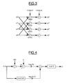
- a hardware implementation of an address calculator allowing determine the address q, i.e. the angle number in the memory dead (q 0 corresponding to a zero angle) is illustrated in Figure 4.
- the address calculator comprises a first multiplier intended to multiply the input data of rank z by the number 4 / N so as to determine the angular sector p.
- a subtractor then makes it possible to subtract from p the number n, so as to obtain a number of log 2 (N) bits. This number is multiplied by i (equal to z modulo N / 4 in the case where the radix is equal to 4).
- a multiplier log 2 (N) xlog 2 (N-2) modulo N then makes it possible to determine the angle value q.
- FIGS. 5 to 8d an embodiment of a calculation device according to the invention, with pipelined architecture, and able to perform the Fourier transform of an input symbol of size equal to 16 by a complex sine waveform of period not.
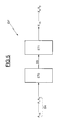
- This pipelined architecture device comprises two stages of treatment with radix 4, ET0 and ET1. According to the invention, only the stage ET0 simultaneously performs Fourier transform calculations relating to this first stage, and the product by the sine waveform complex.
- the processing stage ET 1 performs only processing of conventional Fourier transform, in accordance with the illustrated operator in figure 1.
- the input stage ET0 receives streams of symbols or data blocks BA, comprising respectively sixteen data A 0 -A 15 .
- the output of stage ET0 delivers successive blocks BB of four data which are processed in stage AND 1.
- This stage ET 1 delivers the output symbol X 15 ... X 4 X 0 corresponding to the direct Fourier transformation of the product of the input symbol BA by the complex sine waveform of period n.
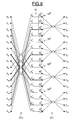
- the radix 4 processing stage then performs N / 4 treatments of the butterfly type conforming to the graph of FIG. 2, on N / 4 groups distinct from four data formed respectively by a data of the first segment and peer data from the other three segments.
- the stage ETO performs a first butterfly type processing on the group formed of the data A 0 , A 4 , A 8 and A 12 , a second butterfly type processing on a second group of data formed by data A 1 , A 5 , A 9 and A 13 and so on until a fourth butterfly-type processing on the fourth group of data formed by data A 3 , A 7 , A 11 and A 15 .
- step ET1 will successively perform a butterfly type treatment in accordance with graph of figure 1 on the four data of each input block BB, so as to obtain intermediate data B *, then output that is actually, in this case, the result of the Fourier transform of the product of the complex exponential of period n by the input data A.
- the reference MTE designates the means of elementary processing of a radix 4 processing stage of the device DF.
- These MTE means include an input terminal receiving the stream INS of the different data blocks coming either from a means outside the device if the stage considered is the first (in this case the different blocks represent the different symbols on which will be done the Fourier transform of the product of each symbol by the complex exponential), or from the previous stage.
- the data contained in each of the blocks received are delivered at the rate of one first clock signal SMCK.
- the MTE processing means are, meanwhile, clocked by a basic clock signal MCK whose frequency is twice the frequency of the signal SMCK, which is four times greater depending on the means of MTE processing receive during each cycle the SMCK signal either the real part and the imaginary part of each datum, or only the real part or the imaginary part.
- the OUS output data stream is delivered to a terminal exit from this processing stage.
- the elementary processing means MTE receive a first STBL control signal from either external means of the device if the stage considered is the first, either from the previous floor.
- This STBL signal indicates, for example during its passage to state "1", the reception of the first data of a block.
- the MTE means deliver to the stage according to a second signal STMX control indicating, for example during its transition to the state "1", the transmission of the first output data from the processing of said input block.
- the STBL signal received by the current stage is then the STNX signal emitted by the previous stage.
- the floor of radix 4 processing includes elementary storage means composed here of a single access random access memory MM looped back to the basic MTE processing means by via a first REG1 register or flip-flop connected to the MM memory output, and through a second register or REG2 flip-flop connected to the MM memory input.
- Memory MM is commanded in writing / reading by an R / W signal. When this signal is "1" for example, it is a read and when it is "0", it is a writing.
- the memory is addressed by an ADD address pointer.
- the clock signal from MCK database either write access or read access from memory MM. Therefore, at each cycle of the first signal the SMCK clock is read access followed by access writing memory.
- the processing stage at radix 4 is the first stage ET0 and that it is of a first type within which one does not carry out data dynamics calculations.
- the storage capacity of the means of elementary memorization of the processing stage is equal to 3N / 4 data.
- the storage capacity of memory is equal to N / 4-1 words of three data while each register REG1, REG2 is able to store a word of three data.
- MM memory can therefore be represented as a matrix of N / 4-1 rows and 3 columns.
- the elementary processing means include a module MD1 complex adder / subtractor used to calculate the intermediate data according to the formulas deduced from FIGS. 2 and 3, as well as an MD2 multiplier module allowing to multiply these intermediate data by appropriate coefficients W.
- the output of the multiplier module therefore delivers the OUS output data stream.
- the four outputs 0, 1, 2, 3 of the MD1 module respectively deliver the intermediate data A i K * , A N / 4 + i K * , A N / 2 + i K * , A 3N / 4 + i K * from four intermediate segments.
- the floor input terminal receiving the INS data stream input, as well as the three outputs 1, 2, 3 of the first register REG1 are respectively connected to the four inputs 0, 1, 2, 3 of the MD1 adder module.
- the entrance terminal on this floor is also connected to the entrance 0 of a first multiplexer with four MX1 inputs including three outputs are connected to the three entries in the REG2 register.
- the other three inputs 1, 2 and 3 of the first multiplexer MX 1 are both connected to the three outputs 1, 2, 3 of the REG1 register and to the three outputs 1, 2 and 3 of the MD1 module.
- the output 0 of the MD1 module is connected to the input 0 of a second multiplexer MX2 with four inputs whose output is connected to the input of the MD2 multiplier module.
- the other three entries 1, 2 and 3 of the second multiplexer are connected to the three outputs of the first REGI register.
- each input block is indexed by a first counter (write counter) WRC modulo N and counting 0 to N-1 for example at the frequency of the first clock signal SMCK.
- the output data is indexed from 0 to N-1 by a second modulo N counter, or RDC reading counter, counting also for example from 0 to N-1 at the frequency of the first signal clock.
- first STBL control signal indicating receipt of the first block data
- second control signal STNX signaling the emission of the first output data
- WRC write counter controls first multiplexer MX1.
- the three entries 1, 2, 3 of the REG2 register receive respectively the data available at the entrance to the floor, and the values available at outputs 2 and 3 of the REG1 register.
- the three entries 1, 2, 3 of register REG2 receive respectively the value available at output 1 of register REG1, the data available at the input of the processing stage and the value available at output 3 of the REG1 register.
- the entries 1, 2 and 3 of register REG2 receive respectively the value issued at output 1 of register REG1, the value delivered at output 2 REG1, and the data available at the entrance to the treatment.
- the three entries 1, 2 and 3 of the REG2 register respectively receive the values delivered by outputs 1, 2 and 3 of the MD1 module.
- the REG2 register then stores the three data which will be written to the next clock cycle in the memory MM.
- the RDC counter controls the MX2 multiplexer.
- the MD2 multiplier module will receive the value delivered by the output 0 of module MD1.
- the module MD2 When the RDC counter counts from N / 4 to N / 2-1, the module MD2 will receive the value available at output 1 of the REG1 register.
- the module MD2 When the RDC counter counts from N / 2 to 3N / 4-1, the module MD2 will receive the value available at output 2 of the REG1 register.
- the module MD2 When the RDC counter counts from 3N / 4 to N-1, the module MD2 will receive the value available at output 3 of the REG1 register.
- the address signal ADD of the memory MM is delivered by a modulo N / 4-1 counter (not shown here for the purpose of simplification) and counting for example from 0 to N / 4-2 at the frequency of first clock signal SMCK.
- the sine and cosine values of the coefficients W complexes which will be used in the MD2 module, are stored in read-only memory MM1 addressed by the computer output ADC address such as that illustrated in Figure 4.
- the memory MM contains the data A i K , A N / 4 + i K , and A N / 2 + i K of the first three segments of the block K which have been stored as and when they are received, that is, as the WRC counter counted from 0 to 3N / 4-1.
- i varies from 0 to N / 4-1 to the rhythm of the WRC counter.
- the stage receives successively as input the data A 3N / 4 + i K of the fourth segment of the block.
- these data are not stored in the memory MM and are used with the homologous data of the first three segments to calculate the intermediate data A i K * , A N / 4 + i K * , A N / 2 + i K * and A 3N / 4 + i K * of the four intermediate segments.
- the intermediate data A i K * of the first intermediate segment are not stored in the memory MM and are directly transmitted to the multiplier module MD2.
- next step i.e. when the WRC counter count from 0 to N / 4-1 corresponding to the reception of data from the first segment of block K + 1, we successively extract from the memory words ML2i (i varying from 0 to N / 4-1) corresponding to previous words of writing MEli.
- the memory MM again contains the data of the first three segments of block K + 1 and a new complete writing / reading cycle can start again.
- the hardware structure of the ET1 processing stage differs simply the structure of stage ET0 as illustrated on the FIG. 8, by the fact that the operator MD1 conforms to the graph of the Figure 1.
- the read-only memory MM 1 also contains the values of sines and cosines of classical complex coefficients W for the computation of a Fourier transform. MM1 memory can then be addressed directly by the RDC read counter.
- the invention simply performs the direct Fourier transform of the product of the input symbol by the complex sine waveform by overcoming the calculation noise generated by a multiplier additional arranged before the entrance floor.
- the surplus of equipment is limited and basic treatments can be performed without any other rounding mechanism than those already existing conventionally in the processing stages implementing Fourier transforms.
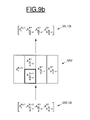
- the MM memory stores all data from the four segments of a block current K. We assume that this was done just before step illustrated in Figure 9a.
- the data of the first segment of the next block K + 1 is replace in the first column the data of the first segment of block K while the intermediate data of the last three intermediate segments of block K are substituted in the other three columns of the matrix, to the data of the last three segments of the block K.
- next step that is to say when the counter counts from N / 4 to N / 2-1, the words ML12i are extracted from the memory and the data of the second segment of the next block K + 1 is substituted to the intermediate data of the second segment of block K, the others intermediate data being rewritten in the memory MM (words ME12i).
- the memory contains all the data of the next block K + 1 1 allowing a recalculation on cropped data.
- the complex coefficients are equal to e 2jq ⁇ / N , where q is equal to (pn) i modulo N, with i equal to z modulo N / 2 and varying from 0 to N / 2-1, and p being 0 or 1.
Landscapes
- Physics & Mathematics (AREA)
- Mathematical Physics (AREA)
- Engineering & Computer Science (AREA)
- General Physics & Mathematics (AREA)
- Computational Mathematics (AREA)
- Mathematical Analysis (AREA)
- Mathematical Optimization (AREA)
- Pure & Applied Mathematics (AREA)
- Data Mining & Analysis (AREA)
- Theoretical Computer Science (AREA)
- Discrete Mathematics (AREA)
- Algebra (AREA)
- Databases & Information Systems (AREA)
- Software Systems (AREA)
- General Engineering & Computer Science (AREA)
- Complex Calculations (AREA)
Abstract
Description
- un module additionneur/soustracteur complexe du type papillon, modifié compte tenu du rang z de la donnée au sein du symbole d'entrée et de la valeur de n modulo r, où r désigne le radix de la transformée de Fourier élémentaire associée au premier étage,
- une mémoire contenant N coefficients complexes respectivement égaux à e2jqπ/N, q étant un entier,
- des moyens d'élaboration aptes à déterminer l'entier q à partir du rang z de la donnée d'entrée (z variant de 0 à N-1), du secteur p dans lequel se situe la donnée d'entrée (p variant de 0 à r-1) et de n, et
- un multiplieur apte à effectuer les produits des coefficients successivement extraits de la mémoire, par les valeurs de sortie successivement délivrées par le module additionneur/soustracteur complexe.
- la figure 1 illustre un opérateur classique de transformée de Fourier en forme de papillon à radix 4;
- la figure 2 illustre un opérateur complexe du type papillon selon l'invention;
- la figure 3 illustre plus précisément le module additionneur/ soustracteur complexe de l'opérateur de la figure 2;
- la figure 4 est une implémentation matérielle selon l'invention, permettant d'adresser des coefficients complexes utilisables à la fois pour le calcul de transformée de Fourier et pour la multiplication complexe par la forme d'onde sinusoïdale de période n;
- la figure 5 est un synoptique schématique d'un dispositif selon l'invention à architecture pipelinée à deux étages de traitement;
- la figure 6 illustre les traitements de type papillon effectués selon l'invention dans ces étages;
- la figure 7 est une représentation schématique de l'architecture matérielle d'un étage de traitement du dispositif de la figure 1;
- la figure 8 illustre plus en détail certains des moyens illustrés sur la figure 7 et implémentés dans le premier étage de traitement;
- les figures 9a à 9d illustrent très schématiquement la configuration d'une mémoire d'un dispositif selon l'invention à architecure pipelinée et la mise en oeuvre de ce dispositif dans le cas d'un recadrage de données au sein d'un étage de traitement à radix 4 à architecture pipelinée;
- la figure 10 illustre un opérateur classique de transformée de Fourier en forme de papillon à radix 2; et
- la figure 11 illustre un opérateur de type papillon à radix 2 selon l'invention.
FFT (exp(2jπ nz/N)Az) dans laquelle FFT désigne l'opérateur transformée de Fourier directe, N est la taille du symbole d'entrée A (N = NO = 2048 par exemple), et dans laquelle n est un entier désignant la période de la forme d'onde sinusoïdale complexe destinée à être multipliée aux données Az (z variant de 0 à N-1) du symbole d'entrée.
| f(n,z) | z=0 à N/4-1 | z=N/4 à N/2-1 | z=N/2 à 3N/4-1 | z=3N/4 à N-1 |
| n=0 mod 4 | 1 | 1 | 1 | 1 |
| n=1 mod 4 | 1 | j | -1 | -j |
| n=2 mod 4 | 1 | -1 | 1 | -1 |
| n=3 mod 4 | 1 | -j | -1 | j |
| f(n,z) | z=0 à N/2-1 | z=N/2 à N-1 |
| n=0 mod 2 | 1 | 1 |
| n=1 mod 2 | 1 | -1 |
Claims (5)
- Dispositif électronique, comprenant des moyens de traitement aptes à calculer la transformée de Fourier directe ou inverse du produit d'un symbole complexe d'entrée de taille N par une forme d'onde sinusoïdale complexe de période n, à partir de traitements élémentaires du type papillon correspondant à plusieurs étages d'un graphe de calcul en forme générale de papillon, caractérisé par le fait que n est un entier inférieur à N, et par le fait que les moyens de traitement comportent des premiers moyens de traitement élémentaires (MTE) aptes à effectuer simultanément ledit produit et les calculs de transformée de Fourier relatifs au premier étage (ET0) du graphe.
- Dispositif selon la revendication 1, caractérisé par le fait que les premiers moyens de traitement élémentaires comportent un module additionneur/soustracteur complexe (MD1) du type papillon modifié compte tenu du rang z de la donnée au sein du symbole d'entré (A) et de la valeur de n modulo r, où r désigne le radix de la transformée de Fourier élémentaire associée au premier étage (ET0), une mémoire (MM1) contenant N coefficients complexes respectivement égaux à e2jqπ/N, q étant un entier, des moyens d'élaboration (ADC) aptes à élaborer l'entier q à partir du rang z de la donnée d'entrée, du secteur p dans lequel se situe la donnée d'entrée, p variant de 0 à r-1, et de n, ainsi qu'un multiplieur (MD2) apte à effectuer les produits des coefficients successivement extraits de la mémoire (MM1) par des valeurs de sortie successivement délivrées par le module additionneur/soustracteur complexe (MD1).
- Dispositif selon la revendication 2, caractérisé par le fait que, la transformée de Fourier étant directe, l'entier q est égal à (p-n)i modulo N, où i est égal à z modulo N/r, et les moyens d'élaboration (ADC) comportent avantageusement un premier multiplieur calculant le secteur p en effectuant le produit du rang z de la donnée d'entrée par le rapport r/N.
- Dispositif selon la revendication 2 ou 3, caractérisé par le fait que le radix r est égal à 2 ou 4.
- Dispositif selon l'une des revendications précédentes, caractérisé par le fait qu'il est à architecture pipelinée, et par le fait que les premiers moyens de traitement élémentaires sont incorporés dans le premier étage (ETO) du dispositif.
Applications Claiming Priority (2)
| Application Number | Priority Date | Filing Date | Title |
|---|---|---|---|
| FR9900770 | 1999-01-25 | ||
| FR9900770A FR2788869B1 (fr) | 1999-01-25 | 1999-01-25 | Dispositif electronique de calcul de la transformee de fourier directe ou inverse du produit d'un symbole complexe par une forme d'onde sinusoidale complexe, en particulier a architecture dite "pipelinee" |
Publications (1)
| Publication Number | Publication Date |
|---|---|
| EP1022661A1 true EP1022661A1 (fr) | 2000-07-26 |
Family
ID=9541180
Family Applications (1)
| Application Number | Title | Priority Date | Filing Date |
|---|---|---|---|
| EP00400169A Withdrawn EP1022661A1 (fr) | 1999-01-25 | 2000-01-21 | Dispositif de calcul de la transformée de Fourier directe ou inverse du produit d'un symbole complexe par une forme d'onde sinusoídale complexe |
Country Status (3)
| Country | Link |
|---|---|
| US (1) | US6564236B1 (fr) |
| EP (1) | EP1022661A1 (fr) |
| FR (1) | FR2788869B1 (fr) |
Families Citing this family (1)
| Publication number | Priority date | Publication date | Assignee | Title |
|---|---|---|---|---|
| US20050015420A1 (en) * | 2003-07-18 | 2005-01-20 | Gibb Sean G. | Recoded radix-2 pipeline FFT processor |
Family Cites Families (5)
| Publication number | Priority date | Publication date | Assignee | Title |
|---|---|---|---|---|
| FR2315809A1 (fr) * | 1975-06-24 | 1977-01-21 | Trt Telecom Radio Electr | Systeme de transmission des signaux auxiliaires d'un groupe de voies telephoniques d'un multiplex a repartition en frequence |
| FR2772950B1 (fr) * | 1997-12-19 | 2000-03-17 | St Microelectronics Sa | Dispositif electronique de calcul d'une transformee de fourier a architecture dite "pipelinee" et procede de commande correspondant |
| CA2225231C (fr) * | 1997-12-19 | 2004-03-02 | Rui R. Wang | Detection de frequence utilisant des techniques de transformation fourier discretes |
| US6393066B1 (en) * | 1999-02-26 | 2002-05-21 | Trw Inc. | Efficient digital channelizer system and method of operation thereof |
| US6792441B2 (en) * | 2000-03-10 | 2004-09-14 | Jaber Associates Llc | Parallel multiprocessing for the fast fourier transform with pipeline architecture |
-
1999
- 1999-01-25 FR FR9900770A patent/FR2788869B1/fr not_active Expired - Fee Related
-
2000
- 2000-01-21 EP EP00400169A patent/EP1022661A1/fr not_active Withdrawn
- 2000-01-25 US US09/491,001 patent/US6564236B1/en not_active Expired - Lifetime
Non-Patent Citations (2)
| Title |
|---|
| FLIEGE: "Orthogonal Multiple Carrier Data Transmission", EUROPEAN TRANSACTIONS ON TELECOMMUNICATIONS AND RELATED TECHNOLOGIES, vol. 3, no. 3, May 1992 (1992-05-01) - June 1992 (1992-06-01), Milano, IT, pages 255 - 264, XP000304924 * |
| SHOUSHENG HE ET AL: "Designing pipeline FFT processor for ODFM (de)modulation", 1998 URSI INTERNATIONAL SYMPOSIUM ON SIGNALS, SYSTEMS AND ELECTRONICS - CONFERENCE PROCEEDINGS, 29 September 1998 (1998-09-29) - 2 October 1998 (1998-10-02), Pisa, IT, pages 257 - 262, XP002120095 * |
Also Published As
| Publication number | Publication date |
|---|---|
| FR2788869A1 (fr) | 2000-07-28 |
| FR2788869B1 (fr) | 2001-04-13 |
| US6564236B1 (en) | 2003-05-13 |
Similar Documents
| Publication | Publication Date | Title |
|---|---|---|
| EP0154341B1 (fr) | Processeur de calcul d'une transformée discrète du cosinus | |
| EP0154340A1 (fr) | Processeur de calcul d'une transformée discrète inverse du cosinus | |
| EP0924627B1 (fr) | Processeur de calcul d'une transformation rapide de Fourier à architecture dite "pipelinée" | |
| EP0171305A1 (fr) | Circuit de calcul de la transformée de Fourier discrète | |
| EP0924626B1 (fr) | Processeur de calcul d'une transformation rapide de Fourier à architecture dite "pipelinée" | |
| EP0437876B1 (fr) | Multiplieur série programmable | |
| EP1061704B1 (fr) | Procédé et dispositif de calcul d'une transformation rapide de Fourier pour une demodulation OFDM | |
| WO2000026790A1 (fr) | Memoire a acces vectoriel | |
| EP0190514B1 (fr) | Dispositif de test en ligne de circuit de calcul de la transformée de Fourier discrète, et circuit comportant un tel dispositif | |
| EP0667969A1 (fr) | Dispositif electronique de calcul d'une transformee de fourier et procede pour minimiser la taille des chemins de donnees internes d'un tel dispositif | |
| EP0237382A1 (fr) | Dispositif de transformée en cosinus d'un signal numérique échantilloné | |
| FR2788869A1 (fr) | Dispositif electronique de calcul de la transformee de fourier directe ou inverse du produit d'un symbole complexe par une forme d'onde sinusoidale complexe, en particulier a architecture dite "pipelinee" | |
| EP0476592A2 (fr) | Générateur d'adresses pour la mémoire de données d'un processeur | |
| FR2741977A1 (fr) | Appareil pour la transformation d'un cosinus discret bidimensionnel | |
| EP1038236B1 (fr) | Procede de calcul de la transformee de fourier rapide et de la transformee de fourier rapide inverse | |
| CA1278869C (fr) | Processeur de calcul de la transformee de fourier discrete comportant un dispositif de test en ligne | |
| FR2951835A1 (fr) | Dispositif de correction de signaux de consigne et systeme de generation de gradients comportant un tel dispositif | |
| EP1058435B1 (fr) | Procédé et dispositif de calcul d'une transformation de Fourier inverse à architecture dite "pipelinée" | |
| FR2570853A1 (fr) | Dispositif de traitement en temps reel de signal numerique par convolution | |
| EP0718746B1 (fr) | Multiplieur de booth pour fonctions trigonométriques | |
| FR2545629A1 (fr) | Dispositif de calcul pour transformation de fourier rapide | |
| EP4170479B1 (fr) | Circuit intégré comprenant un calculateur matériel et procédé de calcul correspondant | |
| EP0337544B1 (fr) | Procédé et unité de gestion de mots d'adresse | |
| EP0112768B1 (fr) | Opérateur élémentaire, notamment pour multiplieur du type en cascade | |
| FR2632094A1 (fr) | Appareil et methode pour acceder a des donnees emmagasinees dans une memoire de pages |
Legal Events
| Date | Code | Title | Description |
|---|---|---|---|
| PUAI | Public reference made under article 153(3) epc to a published international application that has entered the european phase |
Free format text: ORIGINAL CODE: 0009012 |
|
| AK | Designated contracting states |
Kind code of ref document: A1 Designated state(s): DE FR GB IT |
|
| AX | Request for extension of the european patent |
Free format text: AL;LT;LV;MK;RO;SI |
|
| 17P | Request for examination filed |
Effective date: 20000721 |
|
| AKX | Designation fees paid |
Free format text: DE FR GB IT |
|
| RAP1 | Party data changed (applicant data changed or rights of an application transferred) |
Owner name: STMICROELECTRONICS S.A. |
|
| 17Q | First examination report despatched |
Effective date: 20040910 |
|
| GRAP | Despatch of communication of intention to grant a patent |
Free format text: ORIGINAL CODE: EPIDOSNIGR1 |
|
| STAA | Information on the status of an ep patent application or granted ep patent |
Free format text: STATUS: THE APPLICATION IS DEEMED TO BE WITHDRAWN |
|
| 18D | Application deemed to be withdrawn |
Effective date: 20061220 |