EP1022255B1 - Oxide superconductor - Google Patents
Oxide superconductor Download PDFInfo
- Publication number
- EP1022255B1 EP1022255B1 EP98901014A EP98901014A EP1022255B1 EP 1022255 B1 EP1022255 B1 EP 1022255B1 EP 98901014 A EP98901014 A EP 98901014A EP 98901014 A EP98901014 A EP 98901014A EP 1022255 B1 EP1022255 B1 EP 1022255B1
- Authority
- EP
- European Patent Office
- Prior art keywords
- lead
- domains
- oxide superconductor
- bismuth
- oxide
- Prior art date
- Legal status (The legal status is an assumption and is not a legal conclusion. Google has not performed a legal analysis and makes no representation as to the accuracy of the status listed.)
- Expired - Lifetime
Links
Images


Classifications
-
- B—PERFORMING OPERATIONS; TRANSPORTING
- B82—NANOTECHNOLOGY
- B82Y—SPECIFIC USES OR APPLICATIONS OF NANOSTRUCTURES; MEASUREMENT OR ANALYSIS OF NANOSTRUCTURES; MANUFACTURE OR TREATMENT OF NANOSTRUCTURES
- B82Y30/00—Nanotechnology for materials or surface science, e.g. nanocomposites
-
- C—CHEMISTRY; METALLURGY
- C01—INORGANIC CHEMISTRY
- C01G—COMPOUNDS CONTAINING METALS NOT COVERED BY SUBCLASSES C01D OR C01F
- C01G29/00—Compounds of bismuth
- C01G29/006—Compounds containing bismuth, with or without oxygen or hydrogen, and containing two or more other elements
-
- C—CHEMISTRY; METALLURGY
- C04—CEMENTS; CONCRETE; ARTIFICIAL STONE; CERAMICS; REFRACTORIES
- C04B—LIME, MAGNESIA; SLAG; CEMENTS; COMPOSITIONS THEREOF, e.g. MORTARS, CONCRETE OR LIKE BUILDING MATERIALS; ARTIFICIAL STONE; CERAMICS; REFRACTORIES; TREATMENT OF NATURAL STONE
- C04B35/00—Shaped ceramic products characterised by their composition; Ceramics compositions; Processing powders of inorganic compounds preparatory to the manufacturing of ceramic products
- C04B35/01—Shaped ceramic products characterised by their composition; Ceramics compositions; Processing powders of inorganic compounds preparatory to the manufacturing of ceramic products based on oxide ceramics
- C04B35/45—Shaped ceramic products characterised by their composition; Ceramics compositions; Processing powders of inorganic compounds preparatory to the manufacturing of ceramic products based on oxide ceramics based on copper oxide or solid solutions thereof with other oxides
- C04B35/4521—Shaped ceramic products characterised by their composition; Ceramics compositions; Processing powders of inorganic compounds preparatory to the manufacturing of ceramic products based on oxide ceramics based on copper oxide or solid solutions thereof with other oxides containing bismuth oxide
- C04B35/4525—Shaped ceramic products characterised by their composition; Ceramics compositions; Processing powders of inorganic compounds preparatory to the manufacturing of ceramic products based on oxide ceramics based on copper oxide or solid solutions thereof with other oxides containing bismuth oxide also containing lead oxide
-
- H—ELECTRICITY
- H10—SEMICONDUCTOR DEVICES; ELECTRIC SOLID-STATE DEVICES NOT OTHERWISE PROVIDED FOR
- H10N—ELECTRIC SOLID-STATE DEVICES NOT OTHERWISE PROVIDED FOR
- H10N60/00—Superconducting devices
- H10N60/01—Manufacture or treatment
- H10N60/0268—Manufacture or treatment of devices comprising copper oxide
- H10N60/0828—Introducing flux pinning centres
-
- H—ELECTRICITY
- H10—SEMICONDUCTOR DEVICES; ELECTRIC SOLID-STATE DEVICES NOT OTHERWISE PROVIDED FOR
- H10N—ELECTRIC SOLID-STATE DEVICES NOT OTHERWISE PROVIDED FOR
- H10N60/00—Superconducting devices
- H10N60/80—Constructional details
- H10N60/85—Superconducting active materials
- H10N60/855—Ceramic superconductors
- H10N60/857—Ceramic superconductors comprising copper oxide
-
- C—CHEMISTRY; METALLURGY
- C01—INORGANIC CHEMISTRY
- C01P—INDEXING SCHEME RELATING TO STRUCTURAL AND PHYSICAL ASPECTS OF SOLID INORGANIC COMPOUNDS
- C01P2002/00—Crystal-structural characteristics
- C01P2002/01—Crystal-structural characteristics depicted by a TEM-image
-
- C—CHEMISTRY; METALLURGY
- C01—INORGANIC CHEMISTRY
- C01P—INDEXING SCHEME RELATING TO STRUCTURAL AND PHYSICAL ASPECTS OF SOLID INORGANIC COMPOUNDS
- C01P2004/00—Particle morphology
- C01P2004/60—Particles characterised by their size
- C01P2004/64—Nanometer sized, i.e. from 1-100 nanometer
-
- C—CHEMISTRY; METALLURGY
- C01—INORGANIC CHEMISTRY
- C01P—INDEXING SCHEME RELATING TO STRUCTURAL AND PHYSICAL ASPECTS OF SOLID INORGANIC COMPOUNDS
- C01P2006/00—Physical properties of inorganic compounds
- C01P2006/40—Electric properties
-
- Y—GENERAL TAGGING OF NEW TECHNOLOGICAL DEVELOPMENTS; GENERAL TAGGING OF CROSS-SECTIONAL TECHNOLOGIES SPANNING OVER SEVERAL SECTIONS OF THE IPC; TECHNICAL SUBJECTS COVERED BY FORMER USPC CROSS-REFERENCE ART COLLECTIONS [XRACs] AND DIGESTS
- Y10—TECHNICAL SUBJECTS COVERED BY FORMER USPC
- Y10S—TECHNICAL SUBJECTS COVERED BY FORMER USPC CROSS-REFERENCE ART COLLECTIONS [XRACs] AND DIGESTS
- Y10S505/00—Superconductor technology: apparatus, material, process
- Y10S505/775—High tc, above 30 k, superconducting material
- Y10S505/776—Containing transition metal oxide with rare earth or alkaline earth
- Y10S505/782—Bismuth-, e.g. BiCaSrCuO
Definitions
- bismuth-based superconductors have a large anisotropy of crystal growth rates and thus their oriented structures can be easily attained.
- their application as materials are most advanced, and it may be possible to greatly expand the market of superconductors, if the applications at high temperature in a magnetic field are developed using bismuth-based superconductors.
- the critical temperatures of the samples having the composition in which z is 0.2 were 73 K and 88 K after Thermal treatments a and b, respectively.
- the critical temperature of the unannealed sample was 82 K.
Landscapes
- Chemical & Material Sciences (AREA)
- Engineering & Computer Science (AREA)
- Ceramic Engineering (AREA)
- Organic Chemistry (AREA)
- Materials Engineering (AREA)
- Manufacturing & Machinery (AREA)
- Nanotechnology (AREA)
- Crystallography & Structural Chemistry (AREA)
- General Physics & Mathematics (AREA)
- Physics & Mathematics (AREA)
- Condensed Matter Physics & Semiconductors (AREA)
- Composite Materials (AREA)
- Inorganic Chemistry (AREA)
- Structural Engineering (AREA)
- Inorganic Compounds Of Heavy Metals (AREA)
- Superconductors And Manufacturing Methods Therefor (AREA)
- Superconductor Devices And Manufacturing Methods Thereof (AREA)
Abstract
Description
- The present invention relates to a novel oxide superconductor. In particular, the present invention relates to an oxide superconductor consisting of an oxide which comprises, as constituent metal elements, bismuth, lead, strontium, calcium and copper, and has excellent critical current characteristics in a magnetic field.
- The novel oxide superconductor of the present invention finds a wide variety of applications such as magnets, cables, various devices, etc.
- Hitherto, a number of oxide-base high temperature superconductors have been found. However, all such superconductors have a structure in which superconductive layers consisting of copper-oxygen planes, and non-superconductive layers are alternately laminated, and their electrical magnetic properties have a large anisotropy reflecting such a structure. The crystal systems of such oxide superconductors are tetragonal or orthorhombic, and the copper-oxygen planes form ab planes. A large superconductive current can flow in the direction of such planes, while little current flows in the direction of the c-axis.
- Large-sized oxide-base high temperature superconductive materials consist of polycrystals. In such a case, to flow a large superconductive current, the ab planes of the crystals should be aligned, that is, the crystals are oriented, and the current is allowed to flow in parallel with the ab planes.
- Bismuth-base superconductors have the very large anisotropy of crystal growth rates, and thus the ab planes of the crystals, in which a superconductive current easily flows, grow in the form of a thin plate. Therefore, it is easy to mechanically orient crystals, or to orient crystals during the growth of crystals from a melt by making use of the anisotropy of the surface or interface energy.
- Among bismuth-base superconductors, the Bi2212 and Bi2223 phases, which have high critical temperatures (Tc), have been developed as industrial materials. The ratio of bismuth:strontium:calcium:copper in the former phase is about 2:2:1:2, while such a ratio in the latter phase is about 2:2:2:3. In the latter phase, 10 to 20 atomic % of lead is replaced with bismuth for the acceleration of the crystal growth and the stabilization of the structure.
- The development of wires using such bismuth-base superconductive materials is one of the most advanced areas among the oxide high temperature superconductive materials, because of the easy orientation of crystals. In the case of the Bi2212 phase, a wire, which has a thickness of several ten to several hundred micrometers and consists of plate-form crystals having dense and oriented structures, has been developed by a melting-solidification process on a tape-form metal substrate or in a metal sheath. In the case of the Bi2223 phase, a tape-form metal sheathed wire has been developed, in which the crystals are mechanically oriented in the course of a cold work.
- The critical current density (Jc) of such a wire in the absence of a magnetic field is several ten thousand A/cm2 at the liquid nitrogen temperature (77 K), or several hundred thousand A/ cm2 at a low temperature of 30 K or less. These values are on the highest level among the oxide high temperature superconductors having a length of several meters or longer, and come up to a practical level. At present, current leads, superconductive cables, superconductive magnet devices which can operate at 20 K or less, and the like are developed using such wires, and come into practical use.
- The characteristics of superconductive materials from the viewpoint of applications in the heavy electric industry are that a large amount of a current is allowed to flow through the materials at a high current density without loss and, in this connection, they can generate a strong magnetic field of several teslas or larger. Conventional (classical) metal superconductors inevitably require cooling with liquid helium which is expensive and a valuable resource, since they have a low Tc. However, oxide high temperature superconductors can find applications which require economical and easy cooling with liquid nitrogen or by refrigerators. Therefore, it is expected that superconductive equipment will widely spread. Furthermore, oxide high temperature superconductors are expected to find many applications in the technical fields, which are in a magnetic field or which generate a magnetic field, rather than applications such as cables, etc. in the absence of a magnetic field.
- As stated above, bismuth-based superconductors have a large anisotropy of crystal growth rates and thus their oriented structures can be easily attained. Thus, their application as materials are most advanced, and it may be possible to greatly expand the market of superconductors, if the applications at high temperature in a magnetic field are developed using bismuth-based superconductors.
- However, among oxide superconductors, bismuth-based superconductors are typical materials having a very large electrical magnetic anisotropy, that is, a very weak bond between superconductive layers. Thus, a magnetic flux is hardly pinned in a superconductor in a magnetic field in parallel with the c-axis of a crystal, and the magnetic flux is shifted even by a little current, so that a finite resistance is generated in the superconductor. The influence of thermal fluctuation is small, and pinning effectively functions at a low temperature, and superconductors have a sufficiently high Jc (critical current density) in a high magnetic field. However, at a temperature of 30 K or higher, a magnetic flux very easily moves, and thus Jc sharply drops in a magnetic field. Accordingly, bismuth-based superconductors exhibit practically sufficient Jc only in a very small magnetic field at a high temperature such as the liquid nitrogen temperature. For example, in the case of a Bi2212 phase wire, the intensity of a magnetic field at which Jc becomes 0 (zero) (irreversible magnetic field) is only 0.02 tesla in a magnetic field in parallel with the c-axis at the liquid nitrogen temperature. In addition, in the case of other oxide superconductors having a stronger pinning function, a material having a long length and high Jc has not been developed, since it is difficult to control the orientation of crystals.
- Many attempts have been made to improve the pinning property of bismuth-based superconductors. The introduction of artificial defects by the irradiation with heavy ions or neutrons, which is most effective, is not an industrially applicable method, while the inclusion of Ti, Zr, Hf, etc. in crystals cannot improve the characteristics of superconductors to practical levels.
- It is necessary to introduce effective pinning centers to improve the Jc characteristics of bismuth-based superconductors in a magnetic field. From the practical viewpoint, chemical or mechanical methods are desirable to introduce pinning centers. Examples of pinning centers include non-superconductive deposits, structural defects, grain boundaries of crystals, etc. Since the crystals of bismuth-based superconductors are in the form of thin plates, it is difficult to intentionally add impurities to the superconductors and introduce conductive deposits in the inside of crystals, while the grain boundaries function as weak pinning centers.
- Yttrium- or lanthanum-based superconductors have weak superconductivity around oxygen defects, and the superconductivity is broken near the oxygen defects in a magnetic field having a certain intensity. Such a phenomenon is used to improve a pinning power. However, in the case of bismuth-based superconductors, an essential pinning function is not improved, although anisotropic electrical magnetic characteristics are more or less improved by controlling the amount of oxygen.
- The present inventors have found that, when a part of bismuth atoms are replaced by lead atoms in the Bi2212 phase of a bismuth-based superconductor, domains having a high lead concentration and domains having a low lead concentration form throughout crystals so that plate-form or columnar internal structures form at a lead-rich composition in which a molar ratio of lead to bismuth is 0.2:1 or larger.
- According to the invention as claimed in claim 1, there is provided an oxide superconductor consisting of an oxide which comprises, as constituent metal elements, bismuth, lead, strontium, calcium and copper having a molar ratio of lead to bismuth of at least 0.2:1, preferably from 0.2:1 to 0.7:1, and has a high irreversible magnetic field and a high critical current density. The oxide superconductor has a domain structure comprising domains M having a long-period structure with a period of at least 30 Å (1Å = 0.1 nm), preferably from 30 to 80 Å, in the direction of the b-axis, and domains N having no long-period structure.
- Preferably, the oxide superconductors according to the second aspect of the invention has
- (A) a layered internal structure in which plate-form crystalline domains N having a thickness of about 50 to 1,000 Å and a relatively high lead concentration, and plate-form crystalline domains M having a thickness of about 100 to 2,000 Å and a relatively low lead concentration are alternately laminated in the direction of the b-axis of the crystal, or in a direction which slants from the b-axis towards the a-axis (for example, a direction which slants by 0 to 60 degrees from the b-axis),
- (B) a columnar internal structure in which columnar or cylindroidal crystalline domains having a diameter of about 100 to 2,000 Å and a relatively high lead concentration are present at an interval of about 100 to 2,000 Å in a matrix crystalline domain M having a relatively low lead concentration, or
- (C) both the layered internal structure (A) and the columnar internal structure (B).
- In each case, the lead concentration in the domains N is higher than that in the domain or domains M.
-
- Fig. 1 is an enlarged schematic partial view of one example of the crystal structure of an oxide superconductor according to the present invention.
- Fig. 2 is an enlarged schematic partial view of another example of the crystal structure of an oxide superconductor according to the present invention.
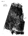
- Fig. 3 is a high-resolution electron micrograph of the crystal structure of the oxide superconductor obtained in Example 1.
- Fig. 4 is a high-resolution electron micrograph of the crystal structure of the oxide superconductor obtained in Example 2.
- In the oxide superconductor of the present invention, a ratio of (bismuth + lead):strontium:calcium:copper is 2:2:1:2 or around such a ratio. For example, a preferred elemental composition can be represented by the formula:
BixPbySrpCaqCu2Oδ
wherein δ is a number of 7 to 9, preferably 7.5 to 8.5; and x, y, p and q are each a positive number, provided that the sum of x and y is from 1.8 to 2.5, preferably from 1.8 and 2.2, in particular 2; the ratio of y to x (y:x) is at least 0.2:1, preferably from 0.2:1 to 0.7:1, and the sum of p and q is from 2.5 to 3.5, preferably 3, and the ratio of p to q (p:q) is preferably 2:1. - Figs. 1 and 2 are enlarged schematic partial views of examples of the crystal structure of the oxide superconductor according to the present invention. In Figs. 1 and 2, the domains N in which a lead concentration is high are shown by gray domains. Such internal structures can be clearly observed with a transmission electron microscope. See undermentioned Examples, and Figs. 3 and 4.
- In the domains N having a high lead concentration and the domain M having a low lead concentration shown in Fig. 1, directions perpendicular to the planes of such domains are in parallel with the direction of the b-axis, or slant by 0 to 60 degrees from the b-axis towards the a-axis. The thicknesses of the domains N and domains M are about 50 to 1,000 Å, and about 100 to 2,000 Å, respectively.
- The domains N having a high lead concentration shown in Fig. 2 have columnar or cylindroidal structures which extend in a direction substantially perpendicular to the ab plane. The diameter of such domains is about 100 to 2,000 Å.
- Such domain structures have interfaces which are perpendicular to the ab plane, or slightly slant from the ab plane. Thus, the interfaces function as effective pinning centers against a magnetic field in parallel with the c-axis, and thus the superconductors of the present invention exhibit a high Jc even at a high temperature in a high magnetic field.
- It has been confirmed that the oxide superconductor of the present invention has a Jc which is several times to several ten times larger than that of conventional bismuth-based superconductors, and an irreversible magnetic field, at a high temperature of 30 K or higher. In particular, an irreversible magnetic field reaches 0.1 tesla at the highest even at the liquid nitrogen temperature (77 K). This indicates that it is possible to assemble a several-tesla grade superconductive magnet cooled with liquid nitrogen, which is designed so that a generated magnetic field is as in parallel with the ab plane as possible (the magnetic field component in the c-axis being at most several percents of the central magnetic field).
- The oxide superconductor of the present invention may be prepared by substantially the same methods as the preparation methods of conventional bismuth-based oxide superconductors except that the amounts of raw materials are adjusted so that the molar ratio of lead to bismuth is in the range defined by the present invention.
- The replacement with lead is a chemical process which can be carried by a general thermal treatment method. Thus, a conventional wire-production method can be readily employed. Accordingly, materials and superconductive equipment, which exhibit good properties at a high temperature in a high magnetic field, can be obtained.
- The bismuth-based superconductor of the present invention has a high Jc even at a high temperature in a high magnetic field, since it contains lead at a high concentration as a whole, the concentration of lead varies from domain to domain, and the interfaces between the domains having a high lead concentration and the domains having a low lead concentration function as pinning centers.
- Bismuth oxide, lead oxide, strontium carbonate, calcium carbonate and copper oxide were weighed so that a molar ratio of bismuth:lead:strontium:calcium:copper was 1.6:0.6:2:1:2 (lead:bismuth = 0.375:1), and mixed. Then, the mixture was calcined at 820°C in an air for 48 hours.
- The sintered powder was press molded in the form of a cylinder having a diameter of 6 mm, and heated by a floating-zone melting method using an infrared condensing furnace to form a single crystal. The obtained single crystal was cleaved and cut to obtain three pieces each having a size of 1 mm x 1 mm x 0.05 mm, which are labeled A, B and C, respectively.
- Samples A and B were sealed in a respective quartz tube under 1 atm. of oxygen and 0.0001 atm. of oxygen, respectively. Sample A was heated at 400°C for 48 hours, while Sample B was heated at 600°C for 24 hours, and then the both samples were quenched. Sample C was not annealed.
- The critical temperatures of Samples A, B and C, which were obtained from the change of susceptibility depending on temperature, were 67 K, 83 K and 87 K, respectively.
- The Jc values of Samples A, B and C, which were measured by a magnetization method at 40 K in a magnetic field of 0.1 tesla in parallel with the c-axis, were 80,000 A/cm2, 70,000 A/cm2 and 70,000 A/cm2, respectively.
- The irreversible magnetic fields of Samples B and C at the liquid nitrogen temperature (77 K) were 0.1 tesla and 0.05 tesla, respectively.
- Samples A, B and C were observed with a transmission electron microscope. All the samples had a structure as shown in Fig. 3, in which domains having a high concentration of lead and no long-period structure (in Fig. 3, the band-form domains N having no stripes) and domains having a low concentration of lead and a long-period structure (in Fig. 3, the band-form domains M having stripes) were alternately laminated in the direction of the b-axis. Here, Fig. 3 is a transmission electron micrograph of Sample C.
- Bismuth oxide, lead oxide, strontium carbonate, calcium carbonate and copper oxide were weighed so that a molar ratio of bismuth:lead:strontium:calcium:copper was 1.5:0.7:2:1:2 (lead:bismuth = 0.467:1), and mixed. Then, the mixture was calcined at 820°C in an air for 48 hours.
- The sintered powder was press molded in the form of a cylinder having a diameter of 6 mm, and heated by a floating-zone melting method using an infrared condensing furnace to form a single crystal. The obtained single crystal was cleaved and cut to obtain a piece having a size of 1 mm x 1 mm x 0.05 mm.
- The critical temperatures of the sample, which was obtained from the change of susceptibility depending on temperature, was 85 K.
- The Jc value of the sample, which was measured by a magnetization method at 30 K in a magnetic field of 0.1 tesla in parallel with the c-axis, was 200,000 A/cm2.
- The sample was observed with a transmission electron microscope. The sample had a structure as shown in Fig. 4, in which the domains having a high concentration of lead and no long-period structure (in Fig. 4, the domains N having no stripes) were grown in the domain having a low concentration of lead and a long-period structure (in Fig. 4, the domain M having stripes) in the direction perpendicular to the ab plane.
- Bismuth oxide, lead oxide, strontium carbonate, calcium carbonate and copper oxide were weighed so that a molar ratio of bismuth:lead:strontium:calcium: copper was (2.2 - z):z:2:1:2 (z = 0 or 0.2), and mixed. Then, the mixture was calcined at 820°C in an air for 48 hours.
- The sintered powder of each composition was press molded in the form of a cylinder having a diameter of 6 mm, and heated by a floating-zone melting method using an infrared condensing furnace to form a single crystal. The obtained single crystal was cleaved and cut to obtain three pieces each having a size of 1 mm x 1 mm x 0.05 mm, for each composition.
- The first sample of each composition was sealed in a quartz tube under 1 atm. of oxygen, and heated at 400°C for 48 hours (Thermal treatment a), while the second sample of each composition was sealed in a quartz tube under 0.0001 atm. of oxygen and heated at 600°C for 24 hours (Thermal treatment b). Then, the both samples were quenched. The third samples of the both compositions were not annealed.
- The critical temperatures of the samples having the composition in which z is zero (0) were 72 K and 87 K after Thermal treatments a and b, respectively. The critical temperature of the unannealed sample was 82 K.
- The Jc value of the sample subjected to Thermal treatment a, which was measured by a magnetization method at 40 K in a magnetic field of 0.1 tesla in parallel with the c-axis, was 1500 A/cm2, while the Jc values of the sample which was subjected to Thermal treatment b and the unannealed sample were both zero (0) at 40 K in the magnetic field of 0.1 tesla.
- The critical temperatures of the samples having the composition in which z is 0.2 were 73 K and 88 K after Thermal treatments a and b, respectively. The critical temperature of the unannealed sample was 82 K.
- The Jc value of the sample subjected to Thermal treatment a, which was measured by a magnetization method at 40 K in a magnetic field of 0.1 tesla in parallel with the c-axis, was 1600 A/cm2, while the Jc value of the sample subjected to Thermal treatment b and the unannealed sample were both zero (0) at 40 K in the magnetic field of 0.1 tesla.
- The microstructures of the samples were observed with a transmission electron microscope. All the samples for Z = 0 and 0.2 had a long-period structure with a uniform period throughout the entire samples.
Claims (6)
- An oxide superconductor consisting of an oxide which comprises, as constituent metal elements, bismuth, lead, strontium, calcium and copper, characterized in that said superconductor has a domain structure comprising domains M having a long-period structure with a period of at least 3 nm (30 Å) in the direction of the b-axis, and domains N having no long-period structure, wherein the molar ratio of lead to bismuth in the oxide superconductor is at least 0.2:1.
- An oxide superconductor according to claim 1, which has an elemental composition represented by the formula:
BixPbySrpCaqCu2O∂
wherein ∂ is a number of 7 to 9; and x, y, p and q are each a positive number, provided that the sum of x and y is from 1.8 to 2.5; the ratio of y to x (y:x) is from 0.2:1 to 0.7:1, and the sum of p and q is from 2.5 to 3.5. - An oxide superconductor according to claim 1, wherein a lead concentration in the domains N is larger than that in the domains M.
- An oxide superconductor according to claim 1, having a layered internal structure in which plate-form crystalline domains N having a thickness of about 5 to 100 nm (50 to 1,000 Å) and a relatively high lead concentration, and plate-form crystalline domains M having a thickness of about 10 to 200 nm (100 to 2,000 Å) and a relatively low lead concentration are alternately laminated in the direction of the b-axis of the crystal, or in a direction which slants from the b-axis towards the a-axis.
- An oxide superconductor according to claim 1, having a columnar internal structure in which columnar_or cylindroidal crystalline domains having a diameter of about 10 to 200 nm (100 to 2,000 Å) and a relatively high lead concentration are present at an interval of about 10 to 200 nm (100 to 2,000 Å) in a matrix crystalline domain M having a relatively low lead concentration.
- An oxide superconductor according to claim 1, having both the layered internal structure of claim 3 and the columnar internal structure of claim 4.
Applications Claiming Priority (3)
| Application Number | Priority Date | Filing Date | Title |
|---|---|---|---|
| JP1514897 | 1997-01-29 | ||
| JP9015148A JPH10212123A (en) | 1997-01-29 | 1997-01-29 | Oxide superconductor |
| PCT/JP1998/000333 WO1998032697A1 (en) | 1997-01-29 | 1998-01-28 | Oxide superconductor |
Publications (3)
| Publication Number | Publication Date |
|---|---|
| EP1022255A1 EP1022255A1 (en) | 2000-07-26 |
| EP1022255A4 EP1022255A4 (en) | 2006-09-06 |
| EP1022255B1 true EP1022255B1 (en) | 2007-10-17 |
Family
ID=11880728
Family Applications (1)
| Application Number | Title | Priority Date | Filing Date |
|---|---|---|---|
| EP98901014A Expired - Lifetime EP1022255B1 (en) | 1997-01-29 | 1998-01-28 | Oxide superconductor |
Country Status (5)
| Country | Link |
|---|---|
| US (1) | US6482775B2 (en) |
| EP (1) | EP1022255B1 (en) |
| JP (1) | JPH10212123A (en) |
| DE (1) | DE69838591T2 (en) |
| WO (1) | WO1998032697A1 (en) |
Families Citing this family (2)
| Publication number | Priority date | Publication date | Assignee | Title |
|---|---|---|---|---|
| WO2003012460A2 (en) * | 2001-08-01 | 2003-02-13 | Southwire Company | Triaxial hts cable |
| US7686151B2 (en) * | 2006-06-01 | 2010-03-30 | Cummins-Allison Corp. | Angled currency processing system |
Family Cites Families (5)
| Publication number | Priority date | Publication date | Assignee | Title |
|---|---|---|---|---|
| JP2827452B2 (en) * | 1990-05-16 | 1998-11-25 | 住友電気工業株式会社 | Ceramic superconductor and method of manufacturing the same |
| CA2076279A1 (en) * | 1991-09-06 | 1993-03-07 | Liang-Sun Hung | Superconductive layer on monocrystalline substrate and process for its preparation |
| JPH07172834A (en) * | 1991-10-08 | 1995-07-11 | Kokusai Chodendo Sangyo Gijutsu Kenkyu Center | Oxide superconducting material and method for producing the same |
| JPH07141940A (en) * | 1993-11-16 | 1995-06-02 | Takeshi Masumoto | Manufacture of superconductive wire of bismuth oxide |
| JP2820082B2 (en) * | 1995-11-06 | 1998-11-05 | 株式会社日立製作所 | Superconducting material |
-
1997
- 1997-01-29 JP JP9015148A patent/JPH10212123A/en active Pending
-
1998
- 1998-01-28 EP EP98901014A patent/EP1022255B1/en not_active Expired - Lifetime
- 1998-01-28 US US09/355,304 patent/US6482775B2/en not_active Expired - Lifetime
- 1998-01-28 DE DE69838591T patent/DE69838591T2/en not_active Expired - Lifetime
- 1998-01-28 WO PCT/JP1998/000333 patent/WO1998032697A1/en not_active Ceased
Also Published As
| Publication number | Publication date |
|---|---|
| EP1022255A1 (en) | 2000-07-26 |
| DE69838591T2 (en) | 2008-07-24 |
| JPH10212123A (en) | 1998-08-11 |
| DE69838591D1 (en) | 2007-11-29 |
| US6482775B2 (en) | 2002-11-19 |
| EP1022255A4 (en) | 2006-09-06 |
| WO1998032697A1 (en) | 1998-07-30 |
| US20020121630A1 (en) | 2002-09-05 |
Similar Documents
| Publication | Publication Date | Title |
|---|---|---|
| KR920005518B1 (en) | Devices and systems based on superconducting material | |
| DE3855246T2 (en) | Superconducting thin film and process for its production | |
| Komatsu et al. | High-Tc superconducting glass-ceramics | |
| EP0660423B1 (en) | Superconductor and method of producing same | |
| EP0277749B1 (en) | Oxide-superconductor | |
| Horii et al. | Growth and anisotropic resistivity of PrBa 2 Cu 4 O 8 and Pr 2 Ba 4 Cu 7 O 15− y single crystals: a direct probe of metallic Cu-O double chains | |
| Mizuguchi et al. | Superconductivity in HEA-type compounds | |
| Matsubara et al. | Superconducting whiskers and crystals of the high T c Bi2Sr2Ca2Cu3O10 phase | |
| EP0510806B1 (en) | Metal oxide material | |
| DE68913787T2 (en) | Insulating oxidic composition for use in a superconducting device. | |
| US5502029A (en) | Laminated super conductor oxide with strontium, calcium, copper and at least one of thallium, lead, and bismuth | |
| US6482775B2 (en) | Oxide superconductor | |
| Volochová et al. | Influence of Gd addition on the microstructure and superconducting properties of YBCO bulk superconductors | |
| Chen et al. | The Nd2O3-SrO-CuO system: compounds and phase relations | |
| US5512542A (en) | Metallic oxide with boron and process for manufacturing the same | |
| Jasim et al. | The effective of pressure on the physical proprieties of Y2Ba4Cu7O15 superconductor | |
| Jin et al. | Structure characteristics of Bi (Pb)-Sr-Ca-Cu-O superconducting whiskers | |
| Isawa et al. | Synthesis of Superconducting Cuprates,(Pb (1+ x)/2Cu (1− x)/2))(Sr1− yCay) 2 (Y1− xCax) Cu2Oz by Means of Encapsulation and Post-Annealing (ECPA) Technique | |
| Goyal et al. | Quasi 1D Layered Nb2PdxSy Superconductor for Industrial Applications | |
| JP2555505B2 (en) | Metal oxide material | |
| JPH04300202A (en) | Superconductor using oxide and its production method | |
| WO1989008076A1 (en) | SUPERCONDUCTIVITY IN A Bi-Ca-Sr-Cu OXIDE COMPOUND SYSTEM FREE OF RARE EARTHS | |
| Suzuki et al. | Synthesis of [Ca2 (Co1-x Cu x) 2O4] y CoO2 Single Crystals and Their Intrinsic Properties | |
| Werfel et al. | Technology, preparation, and characterization | |
| Easterling et al. | The microstructure and properties of high T c superconducting oxides |
Legal Events
| Date | Code | Title | Description |
|---|---|---|---|
| PUAI | Public reference made under article 153(3) epc to a published international application that has entered the european phase |
Free format text: ORIGINAL CODE: 0009012 |
|
| 17P | Request for examination filed |
Effective date: 19990812 |
|
| AK | Designated contracting states |
Kind code of ref document: A1 Designated state(s): CH DE FR GB LI |
|
| RAP1 | Party data changed (applicant data changed or rights of an application transferred) |
Owner name: TAKADA, JUN Owner name: KITAZAWA, KOICHI Owner name: SHIMOYAMA, JUNICHI Owner name: KISHIO, KOHJI Owner name: TERASHIMA, TAKAHITO Owner name: BANDO, YOSHICHIKA Owner name: HIROI, ZENJI Owner name: TAKANO, MIKIO |
|
| A4 | Supplementary search report drawn up and despatched |
Effective date: 20060804 |
|
| 17Q | First examination report despatched |
Effective date: 20061106 |
|
| GRAP | Despatch of communication of intention to grant a patent |
Free format text: ORIGINAL CODE: EPIDOSNIGR1 |
|
| GRAS | Grant fee paid |
Free format text: ORIGINAL CODE: EPIDOSNIGR3 |
|
| GRAA | (expected) grant |
Free format text: ORIGINAL CODE: 0009210 |
|
| AK | Designated contracting states |
Kind code of ref document: B1 Designated state(s): CH DE FR GB LI |
|
| REG | Reference to a national code |
Ref country code: GB Ref legal event code: FG4D |
|
| REG | Reference to a national code |
Ref country code: CH Ref legal event code: EP |
|
| REF | Corresponds to: |
Ref document number: 69838591 Country of ref document: DE Date of ref document: 20071129 Kind code of ref document: P |
|
| REG | Reference to a national code |
Ref country code: CH Ref legal event code: NV Representative=s name: A. BRAUN, BRAUN, HERITIER, ESCHMANN AG PATENTANWAE |
|
| ET | Fr: translation filed | ||
| REG | Reference to a national code |
Ref country code: CH Ref legal event code: NV Representative=s name: BOHEST AG |
|
| PLBE | No opposition filed within time limit |
Free format text: ORIGINAL CODE: 0009261 |
|
| STAA | Information on the status of an ep patent application or granted ep patent |
Free format text: STATUS: NO OPPOSITION FILED WITHIN TIME LIMIT |
|
| 26N | No opposition filed |
Effective date: 20080718 |
|
| REG | Reference to a national code |
Ref country code: CH Ref legal event code: PCAR Free format text: NEW ADDRESS: HOLBEINSTRASSE 36-38, 4051 BASEL (CH) |
|
| REG | Reference to a national code |
Ref country code: FR Ref legal event code: PLFP Year of fee payment: 19 |
|
| REG | Reference to a national code |
Ref country code: FR Ref legal event code: PLFP Year of fee payment: 20 |
|
| PGFP | Annual fee paid to national office [announced via postgrant information from national office to epo] |
Ref country code: FR Payment date: 20161215 Year of fee payment: 20 |
|
| PGFP | Annual fee paid to national office [announced via postgrant information from national office to epo] |
Ref country code: DE Payment date: 20170125 Year of fee payment: 20 Ref country code: CH Payment date: 20170112 Year of fee payment: 20 |
|
| PGFP | Annual fee paid to national office [announced via postgrant information from national office to epo] |
Ref country code: GB Payment date: 20170125 Year of fee payment: 20 |
|
| REG | Reference to a national code |
Ref country code: DE Ref legal event code: R071 Ref document number: 69838591 Country of ref document: DE |
|
| REG | Reference to a national code |
Ref country code: CH Ref legal event code: PL |
|
| REG | Reference to a national code |
Ref country code: GB Ref legal event code: PE20 Expiry date: 20180127 |
|
| PG25 | Lapsed in a contracting state [announced via postgrant information from national office to epo] |
Ref country code: GB Free format text: LAPSE BECAUSE OF EXPIRATION OF PROTECTION Effective date: 20180127 |