EP1020981A2 - Switching power supply unit - Google Patents
Switching power supply unit Download PDFInfo
- Publication number
- EP1020981A2 EP1020981A2 EP00100435A EP00100435A EP1020981A2 EP 1020981 A2 EP1020981 A2 EP 1020981A2 EP 00100435 A EP00100435 A EP 00100435A EP 00100435 A EP00100435 A EP 00100435A EP 1020981 A2 EP1020981 A2 EP 1020981A2
- Authority
- EP
- European Patent Office
- Prior art keywords
- voltage
- power supply
- supply unit
- switching power
- circuit
- Prior art date
- Legal status (The legal status is an assumption and is not a legal conclusion. Google has not performed a legal analysis and makes no representation as to the accuracy of the status listed.)
- Granted
Links
Images



Classifications
-
- H—ELECTRICITY
- H02—GENERATION; CONVERSION OR DISTRIBUTION OF ELECTRIC POWER
- H02M—APPARATUS FOR CONVERSION BETWEEN AC AND AC, BETWEEN AC AND DC, OR BETWEEN DC AND DC, AND FOR USE WITH MAINS OR SIMILAR POWER SUPPLY SYSTEMS; CONVERSION OF DC OR AC INPUT POWER INTO SURGE OUTPUT POWER; CONTROL OR REGULATION THEREOF
- H02M3/00—Conversion of DC power input into DC power output
- H02M3/22—Conversion of DC power input into DC power output with intermediate conversion into AC
- H02M3/24—Conversion of DC power input into DC power output with intermediate conversion into AC by static converters
- H02M3/28—Conversion of DC power input into DC power output with intermediate conversion into AC by static converters using discharge tubes with control electrode or semiconductor devices with control electrode to produce the intermediate AC
- H02M3/325—Conversion of DC power input into DC power output with intermediate conversion into AC by static converters using discharge tubes with control electrode or semiconductor devices with control electrode to produce the intermediate AC using devices of a triode or a transistor type requiring continuous application of a control signal
- H02M3/335—Conversion of DC power input into DC power output with intermediate conversion into AC by static converters using discharge tubes with control electrode or semiconductor devices with control electrode to produce the intermediate AC using devices of a triode or a transistor type requiring continuous application of a control signal using semiconductor devices only
- H02M3/338—Conversion of DC power input into DC power output with intermediate conversion into AC by static converters using discharge tubes with control electrode or semiconductor devices with control electrode to produce the intermediate AC using devices of a triode or a transistor type requiring continuous application of a control signal using semiconductor devices only in a self-oscillating arrangement
- H02M3/3381—Conversion of DC power input into DC power output with intermediate conversion into AC by static converters using discharge tubes with control electrode or semiconductor devices with control electrode to produce the intermediate AC using devices of a triode or a transistor type requiring continuous application of a control signal using semiconductor devices only in a self-oscillating arrangement using a single commutation path
Definitions
- the present invention relates to a switching power supply unit, and more particularly to a switching power supply unit of a self-excitation-type ringing choke converter (hereinafter abbreviated as RCC) system.
- RCC self-excitation-type ringing choke converter
- switching power supply units of the RCC system in which relatively easy construction is possible to obtain high efficiency, have been widely used.
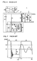
- a structure of such a switching power supply unit will be illustrated referring to Fig. 6.
- reference numeral 1 indicates a switching power supply unit, which has an input circuit 2, a main operation circuit 3, a voltage detection circuit 4, a control circuit 5, an output terminal OUT, and a ground terminal GND.
- the input circuit 2 has a rectifying diode bridge DB, a fuse F, and a filter circuit LF. Both the fuse F and the filter circuit are disposed between an AC power supply and an input end of the rectifying diode bridge DB.
- the main operation circuit 3 has a smoothing capacitor C1 disposed between the output ends a and b of the diode bridge DB of the input circuit 2, a transformer T having a primary winding N1, a secondary winding N2 having the polarity opposite to that of the primary winding N1 and a feedback winding NB with the same polarity as that of the primary winding N1, an FET Q1 as a main switching element connected in series to an end of the primary winding N1 of the transformer T, a starting resistor R1 connected between the other end of the primary winding N1 and the gate as the control terminal of the FET Q1, a resistor R8 connected between the gate and source of the FET Q1, a rectifying diode D1 connected in series to an end of the secondary winding N2 of the transformer T, and a smoothing capacitor C4 connected between an end of the secondary winding N2 and the output terminal.
- a smoothing capacitor C1 disposed between the output ends a and b of the diode bridge DB of the
- the voltage detection circuit 4, which is disposed on the output side of the main operation circuit 3, includes a resistor R5, a light-emitting diode PD on the light-emitting side of a photo coupler PC, a shunt regulator Sr, and resistors R6 and R7.
- the resistor R5, the anode and cathode of the light-emitting diode PD, and the cathode of the shunt regulator Sr are mutually connected in series and are disposed in parallel to the capacitor C4 of the main operation circuit 3.
- the resistors R6 and R7 are also mutually connected in series and are also disposed in parallel to the capacitor C4.
- the node of the resistors R6 and R7 is connected to a reference of the shunt regulator Sr.
- control circuit 5 includes a resistor R9 and a capacitor C3 connected in series between one end of the feedback winding NB and the gate of the FET Q1, a transistor Q2 connected between the gate and source of the FET Q1, a resistor R2 connected between one end of the feedback winding NB and the base of the transistor Q2, a resistor R3 and a capacitor C2 connected in parallel between the base and emitter of the transistor Q2, a resistor R4, a diode D2, and a photo transistor PT on the light-receiving side of the photo coupler PC, which are mutually connected in series between one end of the feedback winding NB and the base of the transistor Q2.
- a voltage is applied to the gate of the FET Q1 via the resistor R1 to turn on the FET Q1.
- a power supply voltage is applied to the primary winding N1 of the transformer T, and then, at the feedback winding NB is generated a voltage of the same direction as that of the voltage generated at the primary winding N1, whereby the FET Q1 is rapidly turned on by a positive feedback. In this situation, excitation energy is charged in the primary winding N1.
- the transistor Q2 when the base potential of the transistor Q2 reaches a threshold, the transistor Q2 is turned on, whereas the FET Q1 is turned off. This permits the excitation energy charged in the primary winding N1 of the transformer T during the ON time of the FET Q1 to be discharged as electric energy via the secondary winding N2.
- the energy is rectified by the diode D1 and is smoothed by the capacitor C4 to be supplied to a load.
- a fly-back voltage VNB is generated at the feedback winding NB. Changes in the fly-back voltage VNB will be illustrated referring to Fig. 7.
- the FET Q1 is turned off and the fly-back voltage VNB is maintained at an almost fixed value to enter the so-called OFF time.
- the voltage of the diode D1 becomes zero, and the fly-back voltage VNB begins to resonate.
- the output voltage of the load is divided by the resistors R6 and R7, and the divided detection voltage is compared with a reference voltage of the shunt regulator Sr.
- the amount of fluctuations in the output voltage is amplified by the shunt regulator Sr, and current flowing to the light-emitting diode PD of the photo coupler PC changes, in which the impedance of the photo transistor PT changes according to the light-emitting amount of the light-emitting diode PD.
- This operation permits the time for charging / discharging the capacitor C2 to be changed, so that the output voltage is regulated.
- switching losses under light load are large, which leads to reduced circuit efficiency.
- the present invention can solve the aforementioned problem and provide a switching power supply unit capable of suppressing increase in switching losses under light load.
- the present invention provides a switching power supply unit including a DC power supply, a transformer having a primary winding, a secondary winding and a feedback winding, and a main switching element connected in series to be turned on by a voltage generated at the feedback winding, so that a DC output can be obtained.
- a voltage dropping circuit for dropping the output voltage is provided, and the output voltage is dropped by the voltage dropping circuit to reduce a fly-back voltage generated at the feedback winding during the OFF time of the main switching, so that the voltage of a control terminal of the main switching element is maintained at a lower value than that of a threshold voltage of the main switching element.
- the voltage dropping circuit there are provided a switching element and a resistor connected in series to the collector thereof to dispose an impedance adjustment circuit for changing impedance determining the output voltage.
- the voltage dropping circuit there is provided a reference-voltage adjustment circuit for changing a reference voltage determining the output voltage.
- the voltage dropping circuit is driven by a signal input from the outside.
- the voltage dropping means permits an output voltage to be dropped.
- the fly-back voltage generated at the feedback winding of the transformer increases or decrease in proportion to the output voltage
- adjusting the dropping level of the output voltage and reducing the fly-back voltage generated during the OFF time of the main switching element allows the voltage of the control terminal of the main switching element to resonate at a lower value than that of a threshold voltage, in which the turn-on of the main switching element by the fly-back voltage can be prevented.
- This operation delays the turn-on of the main switching element and allows the OFF time thereof to be prolonged, in which the oscillation frequency in the switching power supply unit is reduced. As a result, increase in switching losses caused by the rising of the oscillation frequency can be suppressed so that circuit efficiency can be improved.
- the switching element forming the impedance adjustment circuit as the voltage dropping circuit is turned on, in which impedance for determining the output voltage is changed or the reference voltage is changed by impedance generated at the resistor similarly forming the impedance adjustment circuit so as to change the output voltage.
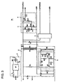
- FIG. 1 A structure of a switching power supply unit according to a first embodiment of the present invention will be illustrated referring to Fig. 1.
- the switching power supply unit 1a shown in the figure is different from the switching power supply unit 1 shown in Fig. 6 in that an impedance adjustment circuit 6 and a DC-DC converter 7 as a voltage dropping circuit for dropping an output voltage VO1 are disposed on the output side of the voltage detection circuit 4.
- an impedance adjustment circuit 6 and a DC-DC converter 7 as a voltage dropping circuit for dropping an output voltage VO1 are disposed on the output side of the voltage detection circuit 4.
- the same parts as those in Fig. 6 or the equivalent parts thereto are given the same reference numerals and the explanation thereof is omitted.
- the impedance adjustment circuit 6 forming the switching power supply unit 1a includes a transistor Q3 as a switching element and resistors R10 and R11.
- the emitter of the transistor Q3 is connected to one end of the secondary winding N2 of a transformer T via a diode D1, whereas the collector thereof is connected to a shunt regulator Sr of the voltage detection circuit 4 via the resistor R10.
- the base of the transistor Q3 is connected to a reception terminal SS via the resistor R11.
- the reception terminal SS is connected to an electronic device as a load.
- the DC-DC converter 7 is well known as a step-up converter, a step-down converter, or a step-up / step-down converter. The detailed explanation of the structure thereof is omitted.
- the switching power supply unit 1a is used in conjunction with a transmission unit (not shown) disposed in the electronic device as a load. That is, if the load of the switching power supply unit 1a e.g., is a facsimile unit, in a so-called waiting period (under light load) in which the power supply of the facsimile unit is turned on, whereas transmission and reception of data are not being performed, a signal outputted from the transmission unit (not shown) disposed in the facsimile unit is applied to the impedance adjustment circuit 6 via the reception terminal SS of the switching power supply unit 1a.
- a transmission unit not shown
- reference character Vref denotes the reference voltage of the shunt regulator Sr
- reference numerals R6, R7, and R10 indicate the resistance values of the resistors R6, R7, and R10.
- VO1 Vref x ⁇ (R6 + R7) / R7 ⁇
- VO1 Vref x (1/R7) x ⁇ R7+(R6 x R10)/(R6+R10) ⁇
- Equation (4) holds only when R10 is infinite.
- the output voltage VO1 drops.
- the absolute value of the fly-back voltage generated at the feedback winding of the transformer is a value in proportion to the value obtained by adding a forward voltage drop of the diode D1 to an output voltage according to the turn ratio of the feedback winding.
- the absolute value of the fly-back voltage VNB is proportional to the output voltage VO1 in order to adjust the level of drop of the output voltage VO1 by the impedance adjustment circuit 6.
- the fly-back voltage VNB generated during the OFF time of the FET Q1 as a switching element is reduced.
- the switching power supply unit 1a is set such that the voltage of the gate as the control terminal of the FET Q1 resonates at a lower value than a threshold value at which the FET Q1 turns on.
- Fig. 2 shows such changes in the fly-back voltage VNB.
- the absolute value of the fly-back voltage VNB during the OFF time is indicated by equation (5) below.
- the symbol NB indicates the turn number of the feedback winding NB of the transformer T
- the symbol N2 indicates the turn number of the primary winding
- the symbol VF indicates a forward voltage of the rectifying diode D1 of the main operation circuit 3.
- (NB / N2) x (VO1 + VF)
- the output VO1 included in equation (5) becomes smaller, whereby the absolute value of the fly-back voltage VNB is reduced.
- the absolute value of the fly-back voltage VNB of the switching power supply unit in accordance with the present invention which is indicated by the symbol Va in Fig. 2, is smaller than that of the conventional switching power supply unit, which is indicated by the symbol Vb in Fig. 7.
- the fly-back voltage VNB starts to resonate at the point-in-time t2, since it is maintained at a relatively low value until the point-in-time t2, amplitude is small and the value of the gate voltage of the FET Q1 is thereby lower than the threshold value Vth, with the result that the turn-on of the FET Q1 by the fly-back voltage VNB is prevented.
- a voltage is applied to the gate of the FET Q1 by the starting circuit (which is referred to as the starting resistor R1 in this embodiment) of the FET Q1 forming the main operation circuit 3 so as to turn on the FET Q1.
- the dropped output voltage VO1 is stepped up to a desired value by the DC-DC converter 7 to an output voltage VO2, which is supplied to a load.
- a DC-DC converter 7 is connected between both ends of a secondary winding N2 of a transformer T and a voltage detection circuit 4.
- An output terminal OUT1 is provided from an impedance adjustment circuit 6, and an output terminal OUT2 is provided from the DC-DC converter 7. From the output terminals OUT1 and OUT2, two output voltages VO1 and VO2 having mutually different values can be obtained.
- the impedance adjustment circuit 6 allows the output voltage VO1 to drop to be supplied to a load. In addition, dropping of the output voltage VO1 leads to reduction in switching losses and improvement in circuit efficiency.
- the DC-DC converter 7 allows the output voltage VO2 to be stepped up to a desired value and to be supplied to the load.
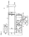
- FIG. 4 a description will be given of a structure of a switching power supply unit in accordance with a second embodiment of the present invention.
- the same parts as those in Fig. 1 and the equivalent parts thereto are given the same reference numerals and the explanation thereof is omitted.
- a fly-back voltage VNB generated at a feedback winding NB is dropped directly by an impedance adjustment circuit 6a.
- the switching power supply unit 1c includes a control circuit 5a, the impedance adjustment circuit 6a, and a DC-DC converter 7.
- a transistor Q4 is disposed as an alternative to the photo coupler PC of the control circuit 5a shown in Fig. 1, and on the base side of the transistor Q4 are disposed resistors R12, R13, R14 and R15, a diode D3, and a capacitor C5.
- the operation of the control circuit 5a is the same as that of a control circuit used in a switching power supply unit of a conventionally known RCC system and the explanation thereof is omitted.
- the impedance adjustment circuit 6a which is connected between both ends of the feedback winding NB of a transformer T, has a transistor Q3.
- the emitter of the transistor Q3 is connected to an end of the feedback winding NB of the transformer T, and the collector thereof is connected to a shunt regulator Sr1 via a resistor R10.
- the shunt regulator Sr1 is connected to the base of the transistor Q4 via the resistor R13 of the control circuit 5a.
- a node of the resistor R10 and the shunt regulator Sr1 is connected to resistors R16 and R17.
- the impedance adjustment circuit 6a includes a rectifying diode D4 and a smoothing capacitor C6.
- the transistor Q3 in the impedance adjustment circuit 6a does not conduct.
- the output voltage VO1 is indicated by equation (6) below.
- the symbol Vref indicates a reference potential of the shunt regulator Sr
- the symbols R10, R16, and R17 indicate the resistance values of the resistors R10, R16, and R17.
- the symbols N2 and NB respectively indicate voltages generated at the secondary winding N2 and feedback winding NB of the transformer T.
- the symbol VF indicates a forward voltage of the diode D1.
- VO1 Vref x ⁇ (R16 + R17)/R17 ⁇ x (N2 / NB) + VF
- VO12 Vref x (1/R17)x ⁇ R17+(R16xR10)/(R16+R17) ⁇
- the switching power supply unit 1c is set such that the level of drop of the output voltage VO1 by the impedance adjustment circuit 6a is adjusted and amplitude is generated within a range below the threshold of the FET Q1 as a main switching element. This allows the OFF time of the FET Q1 to be prolonged so that the oscillation frequency is reduced, as in the case of the first embodiment. Therefore, increase in switching losses due to the rising of the oscillation frequency is suppressed and circuit efficiency can thereby be improved.
- the output voltage VO1 having a value proportional to the value of the fly-back voltage VNB drops.
- the DC-DC converter 7 allows the output voltage VO1 to be stepped up into a desired value to an output voltage VO2, which is supplied to a load.
- a reference voltage adjustment circuit 8 is disposed as a voltage dropping circuit.
- the reference voltage adjustment circuit 8 includes resistors R5, R6, R7, R10, a light-emitting diode PD of the light-emitting side of a photo coupler PC, a transistor Q4, a capacitor C5, a differential amplifier OP, and a voltage source 9.
- the resistor R5, the light-emitting diode PD, and the transistor Q4 are mutually connected in series and are disposed in parallel to a capacitor 4 of a main operation circuit 3.
- the resistors R6 and R7 are mutually connected in series and are similarly disposed in parallel to the capacitor 4.
- the node of the resistors R6 and R7 is connected to an inverting input end of the differential amplifier OP.
- a voltage generated at the voltage source 9 changes in response to a signal from an electronic device as a load.
- the voltage generated at the voltage source 9 is applied to the non-inverting input end of the differential amplifier OP.
- the output end of the differential amplifier OP is connected to the base of the transistor Q4.
- the voltage generated at the voltage source 9 is used as a reference voltage of the differential amplifier OP.
- the voltage generated at the voltage source 9 can be referred to as a variable reference voltage that changes in response to the signal from the electronic device as a load.
- the differential amplifier OP and the transistor Q4 operate as error amplifiers. Both of them operate to make the potential difference between the positive (+) and negative (-) terminals zero, with the result that an output voltage VO2 proportionate to the variable reference voltage can be obtained.
- the impedance adjustment circuit described in each embodiment above operates to drop the voltage generated at the secondary winding NB of the transformer.
- a circuit having any other structure can be replaced for that, as long as the circuit operates in the same way.
- the switching power supply unit having the two output terminals has been illustrated as a switching power supply unit having a plurality of output terminals.
- the present invention can be applied even in the case of a switching power supply unit having three or more output terminals, from each of which an output voltage of a different value can be obtained.
- each of the embodiments described above adopts a case in which a transistor is disposed as a switching element of a voltage dropping circuit
- any other element can be used as an alternative to the transistor, as long as it operates in the same way as the transistor does.
- each of the embodiments described above has shown a case in which under light load (in a waiting time), after the dropping of an output voltage, the DC-DC converter steps up the voltage, in contrast to this, it is possible to use a structure in which the DC-DC converter (a voltage-dropping converter) steps down an output voltage in a waiting time, whereas the stepped-down output voltage is outputted without being stepped up / stepped down and stepping down in a waiting time.
- the DC-DC converter a voltage-dropping converter
- each of the embodiments described above has shown a case in which the DC-DC converter steps up or steps down an output voltage, when the voltage drop in a waiting time is permitted, it is not necessary to provide a DC-DC converter.
Landscapes
- Engineering & Computer Science (AREA)
- Power Engineering (AREA)
- Dc-Dc Converters (AREA)
- Direct Current Feeding And Distribution (AREA)
Abstract
Description
Claims (10)
- A switching power supply unit comprising:a DC power supply (2);a transformer (T) having a primary winding (N1), a secondary winding (N2) and a feedback winding (NB);a main switching element (Q1) connected in series to the primary winding (N1) to be turned on by a voltage generated at the feedback winding (NB); anda voltage dropping circuit (6, 7) for dropping an output voltage (VO1) obtained from the secondary winding (N2) to reduce a fly-back voltage at the feedback winding (NB) so that a voltage at a control terminal of the main switching element (Q1) is maintained at a lower value than that of a threshold voltage of the main switching element (Q1).
- The switching power supply unit of claim 1, wherein the voltage dropping circuit (6, 7) comprises an impedance adjustment circuit (6) for changing impedance determining the output voltage (VO1), the impedance adjustment circuit (6) including a switching element (Q3) having switching terminals and a resistor (R11) connected in series to a switching terminal of the switching element (Q3).
- The switching power supply unit of Claim 1 or 2, wherein the voltage dropping circuit (6, 7) comprises a reference-voltage adjustment circuit for changing a reference voltage determining the output voltage (VO1).
- The switching power supply unit of one of claims 1 to 3, wherein the voltage dropping circuit (6, 7) receives an external signal input and drops the output voltage in response to the signal.
- The switching power supply unit of one of claims 1 to 4, further comprising a DC-DC converter (7) coupled to the secondary winding (N2) for adjusting the output voltage (VO1) of the secondary winding to a desired level.
- The switching power supply unit of claim 5, wherein the output (VO2) of the DC-DC connector (7) and the output (VO1) of the secondary winding are both provided as power supply outputs (OUT1, OUT2).
- The switching power supply unit of one of claims 1 to 6, wherein the voltage dropping circuit (6, 7) is coupled to the secondary winding (N2).
- The switching power supply unit of one of claims 1 to 6, wherein the voltage dropping circuit (6a) is coupled to the feedback winding (NB).
- The switching power supply unit of one of claims 1 to 8, wherein a control output of the voltage dropping circuit (6, 7) is coupled to a control input of a voltage regulator (4) for regulating the output voltage of the secondary winding (VO1).
- The switching power supply unit of claim 3, wherein the reference or voltage adjustment circuit comprises a comparator circuit comparing a variable reference voltage from a variable reference voltage source to an output voltage (VO1) of the secondary winding (N2), an output of the comparator circuit comprising a control signal for a regulator circuit for regulating the output voltage (VO1) of said secondary winding (N2), the variable reference voltage source having a control input for changing a voltage provided by the variable reference voltage source on response to a control signal.
Applications Claiming Priority (4)
| Application Number | Priority Date | Filing Date | Title |
|---|---|---|---|
| JP946799 | 1999-01-18 | ||
| JP946799 | 1999-01-18 | ||
| JP25355199A JP3386016B2 (en) | 1999-01-18 | 1999-09-07 | Switching power supply |
| JP25355199 | 1999-09-07 |
Publications (3)
| Publication Number | Publication Date |
|---|---|
| EP1020981A2 true EP1020981A2 (en) | 2000-07-19 |
| EP1020981A3 EP1020981A3 (en) | 2001-11-21 |
| EP1020981B1 EP1020981B1 (en) | 2003-03-12 |
Family
ID=26344207
Family Applications (1)
| Application Number | Title | Priority Date | Filing Date |
|---|---|---|---|
| EP00100435A Expired - Lifetime EP1020981B1 (en) | 1999-01-18 | 2000-01-10 | Switching power supply unit |
Country Status (6)
| Country | Link |
|---|---|
| US (1) | US6160720A (en) |
| EP (1) | EP1020981B1 (en) |
| JP (1) | JP3386016B2 (en) |
| CA (1) | CA2295382C (en) |
| DE (1) | DE60001590T2 (en) |
| MY (1) | MY117434A (en) |
Cited By (3)
| Publication number | Priority date | Publication date | Assignee | Title |
|---|---|---|---|---|
| DE10138536B4 (en) * | 2001-08-06 | 2007-02-22 | Siemens Ag | Circuit arrangement for power failure bridging in circuits with a switching regulator |
| CN101997419B (en) * | 2000-12-28 | 2012-10-10 | 株式会社村田制作所 | Switching power supply unit |
| CN101753049B (en) * | 2008-12-15 | 2012-12-26 | 佳能株式会社 | Power supply apparatus and image forming apparatus |
Families Citing this family (18)
| Publication number | Priority date | Publication date | Assignee | Title |
|---|---|---|---|---|
| JP3470693B2 (en) | 2000-10-25 | 2003-11-25 | 株式会社村田製作所 | Self-oscillation type switching power supply |
| JP4795583B2 (en) * | 2001-09-20 | 2011-10-19 | 四変テック株式会社 | Power supply |
| US20070109827A1 (en) * | 2003-12-10 | 2007-05-17 | Delacruz Moises | Ac to dc converter circuit |
| JP5042536B2 (en) * | 2006-06-16 | 2012-10-03 | ローム株式会社 | POWER SUPPLY DEVICE AND ELECTRIC DEVICE HAVING THE SAME |
| JP2009042724A (en) | 2007-08-07 | 2009-02-26 | Samsung Sdi Co Ltd | Power supply device and plasma display device including the same |
| TWI422134B (en) * | 2009-07-22 | 2014-01-01 | Mstar Semiconductor Inc | Ultra-low power display control circuit and associated method |
| US8654113B2 (en) * | 2008-09-19 | 2014-02-18 | Mstar Semiconductor, Inc. | Ultra-low-power display control circuit and associated method |
| JP2010220293A (en) | 2009-03-13 | 2010-09-30 | Canon Inc | Switching power supply device |
| CN102474186A (en) * | 2009-07-24 | 2012-05-23 | Nec显示器解决方案株式会社 | switching power supply and electronic device using the same |
| TWI387194B (en) * | 2009-08-14 | 2013-02-21 | Richpower Microelectronics | Apparatus and method for standby power saving of a flyback power converter |
| JP5683241B2 (en) | 2010-12-06 | 2015-03-11 | キヤノン株式会社 | Switching power supply device and image forming apparatus |
| JP5737963B2 (en) * | 2011-01-21 | 2015-06-17 | キヤノン株式会社 | Switching power supply and image forming apparatus having switching power supply |
| KR101972013B1 (en) * | 2011-12-15 | 2019-04-24 | 에이치피프린팅코리아 유한회사 | Switching mode power supply for image forming apparatus, image forming apparatus and method of supplying power by using the same |
| EP2605388B1 (en) * | 2011-12-15 | 2020-12-30 | Hewlett-Packard Development Company, L.P. | Switch mode power supply for an image forming apparatus |
| EP2804303B1 (en) * | 2012-01-11 | 2018-11-28 | Panasonic Corporation | Switching power supply circuit |
| JP6075827B2 (en) | 2012-06-08 | 2017-02-08 | キヤノン株式会社 | Switching power supply device and image forming apparatus |
| US20170358988A1 (en) * | 2014-12-17 | 2017-12-14 | Salcomp Oyj | Switched-mode power supply |
| JP2018110495A (en) * | 2017-01-05 | 2018-07-12 | オンキヨー株式会社 | Switching power supply |
Family Cites Families (11)
| Publication number | Priority date | Publication date | Assignee | Title |
|---|---|---|---|---|
| NL6705849A (en) * | 1967-04-26 | 1967-07-25 | ||
| US4283759A (en) * | 1977-08-01 | 1981-08-11 | Toko, Inc. | Switching regulator |
| NL8502338A (en) * | 1985-08-26 | 1987-03-16 | Philips Nv | SWITCHED POWER SUPPLY SWITCH WITH TWO STATES. |
| JPH02159975A (en) * | 1988-12-09 | 1990-06-20 | Murata Mfg Co Ltd | Self-oscillation type converter |
| DE69328125T2 (en) * | 1992-09-24 | 2000-10-12 | Toshiba Kawasaki Kk | DAMPER CONTROL, SWITCHING POWER SUPPLY AND SATURABLE INDUCTOR USED FOR THIS |
| JPH1098879A (en) * | 1996-09-24 | 1998-04-14 | Matsushita Electric Ind Co Ltd | Switching power supply |
| JP3444468B2 (en) * | 1997-01-29 | 2003-09-08 | 株式会社村田製作所 | DC-DC converter |
| JP3492882B2 (en) * | 1997-04-07 | 2004-02-03 | パイオニア株式会社 | Switching power supply |
| US5841643A (en) * | 1997-10-01 | 1998-11-24 | Linear Technology Corporation | Method and apparatus for isolated flyback regulator control and load compensation |
| JP3381769B2 (en) * | 1997-10-17 | 2003-03-04 | 株式会社村田製作所 | Self-oscillation type switching power supply |
| JP3175663B2 (en) * | 1997-10-17 | 2001-06-11 | 株式会社村田製作所 | Self-oscillation type switching power supply |
-
1999
- 1999-09-07 JP JP25355199A patent/JP3386016B2/en not_active Expired - Fee Related
-
2000
- 2000-01-04 US US09/477,543 patent/US6160720A/en not_active Expired - Lifetime
- 2000-01-06 MY MYPI20000062A patent/MY117434A/en unknown
- 2000-01-10 EP EP00100435A patent/EP1020981B1/en not_active Expired - Lifetime
- 2000-01-10 DE DE60001590T patent/DE60001590T2/en not_active Expired - Lifetime
- 2000-01-14 CA CA002295382A patent/CA2295382C/en not_active Expired - Fee Related
Cited By (3)
| Publication number | Priority date | Publication date | Assignee | Title |
|---|---|---|---|---|
| CN101997419B (en) * | 2000-12-28 | 2012-10-10 | 株式会社村田制作所 | Switching power supply unit |
| DE10138536B4 (en) * | 2001-08-06 | 2007-02-22 | Siemens Ag | Circuit arrangement for power failure bridging in circuits with a switching regulator |
| CN101753049B (en) * | 2008-12-15 | 2012-12-26 | 佳能株式会社 | Power supply apparatus and image forming apparatus |
Also Published As
| Publication number | Publication date |
|---|---|
| MY117434A (en) | 2004-06-30 |
| CA2295382C (en) | 2003-07-22 |
| US6160720A (en) | 2000-12-12 |
| DE60001590T2 (en) | 2004-04-08 |
| EP1020981B1 (en) | 2003-03-12 |
| EP1020981A3 (en) | 2001-11-21 |
| JP3386016B2 (en) | 2003-03-10 |
| CA2295382A1 (en) | 2000-07-18 |
| DE60001590D1 (en) | 2003-04-17 |
| JP2000278946A (en) | 2000-10-06 |
Similar Documents
| Publication | Publication Date | Title |
|---|---|---|
| EP1020981B1 (en) | Switching power supply unit | |
| KR100625598B1 (en) | Switching power supply apparatus | |
| KR100835043B1 (en) | Switching power supply | |
| US5412308A (en) | Dual voltage power supply | |
| US5729448A (en) | Low cost highly manufacturable DC-to-DC power converter | |
| TWI565212B (en) | Flyback-based power conversion apparatus | |
| US8115465B2 (en) | Method and apparatus for a high voltage power supply circuit | |
| US6295211B1 (en) | Switching power supply unit having delay circuit for reducing switching frequency | |
| JP5424442B2 (en) | Device for adjusting diode conduction duty cycle | |
| US7961481B2 (en) | Pulse width modulation control circuit applied to charge output capacitor | |
| JP3475888B2 (en) | Switching power supply | |
| KR101527966B1 (en) | Switch mode power supply and its driving method | |
| US20210021199A1 (en) | Active clamp flyback converter | |
| US6198637B1 (en) | Switching power supply circuit | |
| US6208530B1 (en) | Switching power supply device having main switching element period control circuit | |
| CN113612392B (en) | Switching power supply and control circuit thereof | |
| CN113422524B (en) | Switching power supply and control circuit thereof | |
| KR20080086798A (en) | Method and apparatus for high voltage power supply circuit | |
| US8411476B2 (en) | Charge mode control | |
| US6798671B1 (en) | Switching power supply unit | |
| EP0891036A2 (en) | Switching regulator | |
| JP4414446B2 (en) | Switching power supply circuit | |
| CN213342013U (en) | Switching power supply, circuit board and feedback control circuit thereof | |
| CN110190754B (en) | Converter control circuit and chip | |
| CN120613938A (en) | An isolated DC/DC converter and a method for determining conduction frequency |
Legal Events
| Date | Code | Title | Description |
|---|---|---|---|
| PUAI | Public reference made under article 153(3) epc to a published international application that has entered the european phase |
Free format text: ORIGINAL CODE: 0009012 |
|
| 17P | Request for examination filed |
Effective date: 20000110 |
|
| AK | Designated contracting states |
Kind code of ref document: A2 Designated state(s): DE FR GB Kind code of ref document: A2 Designated state(s): AT BE CH CY DE DK ES FI FR GB GR IE IT LI LU MC NL PT SE |
|
| AX | Request for extension of the european patent |
Free format text: AL;LT;LV;MK;RO;SI |
|
| PUAL | Search report despatched |
Free format text: ORIGINAL CODE: 0009013 |
|
| AK | Designated contracting states |
Kind code of ref document: A3 Designated state(s): AT BE CH CY DE DK ES FI FR GB GR IE IT LI LU MC NL PT SE |
|
| AX | Request for extension of the european patent |
Free format text: AL;LT;LV;MK;RO;SI |
|
| GRAG | Despatch of communication of intention to grant |
Free format text: ORIGINAL CODE: EPIDOS AGRA |
|
| 17Q | First examination report despatched |
Effective date: 20020403 |
|
| GRAG | Despatch of communication of intention to grant |
Free format text: ORIGINAL CODE: EPIDOS AGRA |
|
| GRAH | Despatch of communication of intention to grant a patent |
Free format text: ORIGINAL CODE: EPIDOS IGRA |
|
| AKX | Designation fees paid |
Free format text: DE FR GB |
|
| GRAH | Despatch of communication of intention to grant a patent |
Free format text: ORIGINAL CODE: EPIDOS IGRA |
|
| GRAA | (expected) grant |
Free format text: ORIGINAL CODE: 0009210 |
|
| AK | Designated contracting states |
Designated state(s): DE FR GB |
|
| REG | Reference to a national code |
Ref country code: GB Ref legal event code: FG4D |
|
| REF | Corresponds to: |
Ref document number: 60001590 Country of ref document: DE Date of ref document: 20030417 Kind code of ref document: P |
|
| ET | Fr: translation filed | ||
| PLBE | No opposition filed within time limit |
Free format text: ORIGINAL CODE: 0009261 |
|
| STAA | Information on the status of an ep patent application or granted ep patent |
Free format text: STATUS: NO OPPOSITION FILED WITHIN TIME LIMIT |
|
| 26N | No opposition filed |
Effective date: 20031215 |
|
| PGFP | Annual fee paid to national office [announced via postgrant information from national office to epo] |
Ref country code: DE Payment date: 20140108 Year of fee payment: 15 |
|
| PGFP | Annual fee paid to national office [announced via postgrant information from national office to epo] |
Ref country code: FR Payment date: 20140108 Year of fee payment: 15 |
|
| PGFP | Annual fee paid to national office [announced via postgrant information from national office to epo] |
Ref country code: GB Payment date: 20140108 Year of fee payment: 15 |
|
| REG | Reference to a national code |
Ref country code: DE Ref legal event code: R119 Ref document number: 60001590 Country of ref document: DE |
|
| GBPC | Gb: european patent ceased through non-payment of renewal fee |
Effective date: 20150110 |
|
| PG25 | Lapsed in a contracting state [announced via postgrant information from national office to epo] |
Ref country code: GB Free format text: LAPSE BECAUSE OF NON-PAYMENT OF DUE FEES Effective date: 20150110 Ref country code: DE Free format text: LAPSE BECAUSE OF NON-PAYMENT OF DUE FEES Effective date: 20150801 |
|
| REG | Reference to a national code |
Ref country code: FR Ref legal event code: ST Effective date: 20150930 |
|
| PG25 | Lapsed in a contracting state [announced via postgrant information from national office to epo] |
Ref country code: FR Free format text: LAPSE BECAUSE OF NON-PAYMENT OF DUE FEES Effective date: 20150202 |