Related Application
This application is based upon prior filed copending
provisional application Serial No. 60/115,532 filed
January 12, 1999.
Field Of The Invention
The present invention relates to the field of
semiconductor devices, and, more particularly, to a
capacitor.
Background Of The Invention
Capacitors are used extensively in electronic
devices for storing an electric charge. A capacitor
includes two conductive plates or electrodes separated by
an insulator. The capacitance, or amount of charge held
by the capacitor per applied voltage, depends upon the
area of the plates, the distance between them, and the
dielectric value of the insulator. Capacitors may be
formed within a semiconductor device, such as, for
example, a dynamic random access memory (DRAM) or an
embedded DRAM.
As semiconductor memory devices become more highly
integrated, the area occupied by the capacitor of a DRAM
storage cell is reduced, thus decreasing the capacitance
of the capacitor due to a smaller electrode surface area.
However, a relatively large capacitance is desired to
prevent loss of stored information. Therefore, it is
desirable to reduce the cell dimensions and yet obtain a
high capacitance, which achieves both high cell
integration and reliable operation.
Instead of forming the capacitor on the substrate
surface, capacitors are also formed above the substrate,
i.e., they are stacked above the substrate. The surface
area of the substrate can then be used for forming
transistors. For example, U.S. Patent No. 5,903,493 to
Lee discloses a capacitor formed above a tungsten plug.
The tungsten plug interfaces with an interconnection
line, thus allowing different layers formed above the
substrate to be connected. Such plugs may be anchored or
tapered to secure the plug in the dielectric layer.
Current 0.25 and 0.2 micron semiconductor technology
uses metal-oxide-metal (MOM) capacitors that are formed
above tungsten plugs. However, these plugs can have
surface defects such as seams, recesses, bulges or other
topographical features which may cause MOM capacitor
reliability and yield problems. For example, when the
dielectric adjacent the tungsten plug is polished during
a chemical mechanical polishing (CMP) step, the resulting
tungsten plug may protrude or bulge upwardly above the
dielectric layer.
Summary Of The Invention
In view of the foregoing background, it is therefore
an object of the present invention to provide an
integrated circuit capacitor with metal electrodes and
with increased reliability of the capacitor.
This and other advantages, features and objects in
accordance with the present invention are provided by an
integrated circuit capacitor including a metal plug in a
dielectric layer adjacent a substrate, with the metal
plug having at least one topographical defect in an
uppermost surface portion thereof. A lower metal
electrode overlies the dielectric layer and the metal
plug. The lower metal electrode preferably comprises, in
stacked relation, a metal layer, a lower metal nitride
layer, an aluminum layer, and an upper metal nitride
layer. A capacitor dielectric layer overlies the lower
metal electrode, and an upper metal electrode overlies
the capacitor dielectric layer. An advantage of this
structure is that the stack of metal layers of the lower
metal electrode, will prevent undesired defects at the
surface of the metal plug from adversely effecting device
reliability or manufacturing yield. The aluminum and
metal nitride layers may also desirably provide an etch
stop layer to facilitate manufacturing.
The metal plug preferably comprises tungsten, and
the at least one topographical defect may include at
least one of a recess, a seam and a bulge. The metal
layer of the lower metal electrode preferably comprises a
refractory metal such as titanium. Each of the lower and
upper metal nitride layers of the lower metal electrode
preferably comprises a refractory metal nitride, such as
titanium nitride. Also, the upper metal electrode may
comprise, in stacked relation, a lower metal nitride
layer, an aluminum layer, and an upper metal nitride
layer. Each of the lower and upper metal nitride layers
of the upper metal electrode may also comprise titanium
nitride.
The advantages, features and objects in accordance
with the present invention are also provided by a method
of making an integrated circuit capacitor including the
steps of forming a dielectric layer adjacent a substrate
and forming a metal plug in the dielectric layer. The
forming of the metal plug creates at least one
undesirable topographical defect in an uppermost surface
portion of the metal plug. The method further includes
the step of forming a lower metal electrode overlying the
dielectric layer and the metal plug. The lower metal
electrode may comprise, in stacked relation, a metal
layer, a lower metal nitride layer, an aluminum layer,
and an upper metal nitride layer. A capacitor dielectric
layer is formed over the lower metal electrode, and an
upper metal electrode is formed over the capacitor
dielectric layer.
Brief Description Of The Drawings
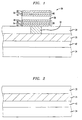
FIG. 1 is a cross-sectional view of an integrated
circuit capacitor in accordance with the present
invention.
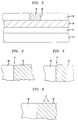
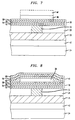
FIGS. 2, 3 and 7-9 are cross-sectional views
illustrating the process steps for forming a capacitor in
accordance with the present invention.
FIGS. 4-6 are enlarged cross-sectional views
illustrating examples of possible defects in the surface
of the metal plug of the capacitor in accordance with the
present invention.
Detailed Description Of The Preferred Embodiments
The present invention will now be described more
fully hereinafter with reference to the accompanying
drawings, in which preferred embodiments of the invention
are shown. This invention may, however, be embodied in
many different forms and should not be construed as
limited to the embodiments set forth herein. Rather,
these embodiments are provided so that this disclosure
will be thorough and complete, and will fully convey the
scope of the invention to those skilled in the art. Like
numbers refer to like elements throughout. The
dimensions of layers and regions may be exaggerated in
the figures for clarity.
Referring initially to FIG. 1, the integrated
circuit MOM capacitor 20 including multilevel metal
electrodes 36, 40 above a metal plug 32, is now
described. The integrated circuit capacitor 20 is formed
above a substrate 24 with an interconnect line 26
adjacent the substrate, and a dielectric layer 28 is on
the interconnection line. The plug 32 is disposed in the
dielectric layer 28. The capacitor 20 includes lower and
upper multilevel metal electrodes 36, 40 and a capacitor
dielectric layer 38 therebetween. The lower metal
electrode 36 contacts the metal plug 32. The second or
capacitor dielectric layer 38 overlies the lower metal
electrode 36, and the upper metal electrode 40 overlies
the second dielectric layer.
The lower metal electrode 36 includes multiple metal
layers 52-58 in stacked relation. The stack includes a
first metal layer 52 and preferably is formed of
titanium. The first metal nitride layer 54 is preferably
formed of a refractory metal nitride, such as titanium
nitride. Layer 56 is a first aluminum layer and layer 58
is a second metal nitride layer also preferably formed of
titanium nitride. Also, the upper metal electrode 40
also illustratively includes multiple metal layers 62-66
in stacked relation. Layer 62 is a third metal nitride
layer and preferably is formed of a refractory metal
nitride such as titanium nitride. Layer 64 is a second
aluminum layer and layer 66 is a fourth metal nitride
layer also preferably formed of titanium nitride.
The capacitor dielectric layer 38 overlies the lower
metal electrode 36 and is formed from any suitable
dielectric, e.g., silicon dioxide, silicon nitride and/or
any material or alloy of material having a suitably large
dielectric constant. Other suitable materials include
tantalum pentoxide and barium strontium titantate, for
example.
As will be described in more detail below, an
advantage of this structure is that the stack of metal
layers 52-58 of the lower metal electrode 36, will
compensate for undesired defects at the surface of the
metal plug 32. The stack will increase integrated
circuit device yield, reduce MOM capacitor leakage and
thus increase the reliability of the MOM capacitor 20.
Additionally, as will also be described below, the first
aluminum layer 56 and the second metal nitride layer 58
are used as an etch stop when patterning and etching the
capacitor dielectric layer 38. Furthermore, the second
aluminum layer 64 and the fourth metal nitride layer 66
can be used as an etch stop for a subsequent via etch.
The interconnect line 26 may include a multilayer
interconnect formed on an insulating layer 42. The
insulating layer 42 is formed on or above the
semiconductor substrate 24. The semiconductor substrate
24 may include a plurality of active devices, such as
transistors, which are connected together into functional
circuits by the interconnect line 26. The multilayer
interconnect may include a conductive capping layer, a
bulk conductor, and an electromigration barrier layer
(not shown) as would readily be appreciated by those
skilled in the art. Additionally, an anti-reflective
coating (ARC), such as titanium nitride, may be formed on
the interconnect line 26.
The integrated capacitor 20 is electrically
connected to the interconnect line 26 by the metal plug
32. The metal plug 32 preferably includes tungsten or
any suitable, electrically conductive material such as
aluminum, titanium or titanium nitride.
A method for making the integrated circuit MOM
capacitor 20 including the multilevel metal electrodes
36, 40 above a metal plug 32, as described above, will
now be further discussed with reference to FIGS. 2-9.
Referring to FIG. 2, the semiconductor substrate 24 is
preferably silicon, or may be silicon or a polysilicon
layer or structure formed on the substrate. A plurality
of devices, such as transistors (not shown), are formed
in the substrate 24 using well known techniques. Next,
the dielectric layer 42, such as a doped or undoped
silicon dioxide, is formed over the substrate 24 with
well known techniques, such as thermal growth or
deposition.
Next, the interconnection line 26 is formed on the
dielectric layer 42. As an example, an approximately 450
nm thick aluminum alloy layer comprising approximately 1%
copper may be formed on a titanum layer using well known
techniques, such as sputtering. An aluminum alloy layer
has low resistivity and is readily procured; however,
other low resistance materials may be used as a bulk
conductor in the interconnect line 26, as will be
appreciated by those skilled in the art. As discussed
above, the interconnect line 26 may be a multilayer
interconnect as would readily be appreciated by those
skilled in the art. Additionally, an anti-reflective
coating (ARC), such as titanium nitride, may be formed on
the interconnect line 26.
The dielectric layer 28, such as a doped silicon
dioxide, is formed over the interconnect line 26. Any
well known technique can be used to form the dielectric
layer 28, such as chemical vapor deposition (CVD).
Referring to FIG. 3, a photoresist layer (not shown) is
formed and patterned over the dielectric layer 28 using
well known photolithography techniques to define the
location where a via hole 50 is to be formed. Next, the
exposed portions of the dielectric layer 28 are etched.
The via hole 50 is etched until the interconnect line 26
is exposed. In one embodiment, a directional reactive
ion etch (RIE) is used to form the via hole 50. The via
hole 50 could be etched using standard etch conditions.
Typical etchants are C4F8/CO/Ar/O2 mixtures.
The via hole 50 is filled with a conductive
material, preferably tungsten, using well known
techniques for forming the metal plug 32. Prior to
forming the plug 32, a nucleation layer, such as titanium
nitride or tantalum nitride, may be sputter deposited on
the side walls of the via hole 50, as would be
appreciated by those skilled in the art. Also, a thin
adhesion/barrier layer, such as titanium or titanium
nitride can be blanket deposited into the via hole 50
using well known techniques such as sputtering. The
conductive material is deposited into the via hole 50
until the via hole 50 is filled. A chemical-mechanical
polishing technique may be used to etch back the
adhesion/barrier metals and any conductive material
deposited on the dielectric layer 28. Alternatively, a
metal layer may be deposited on the interconnect line 26
and then patterned and etched to form the metal plug 32.
Here, the dielectric layer 28 would then be formed over
the metal plug 32.
The dielectric layer 28 is preferably planarized at
this time by chemical-mechanical polishing or etch back
to form a planar top surface. The resulting thickness of
the dielectric layer 28 should be thick enough after
planarization to provide adequate electrical isolation of
the interconnect line 26 from a subsequent level of
metallization. For example, an approximate thickness of
400 to 600 nm provides suitable isolation.
Referring now to FIGS. 4-6, after the formation of
the metal plug 32 and the dielectric layer 28, defects d
may be exist at the surface of the metal plug 32. For
example, as shown in FIGS. 4 and 6, a seam or recess d
may exist at the boundary of the metal plug 32 and the
dielectric layer 28. As illustrated in FIG. 5, a bulge
or hump d may be formed at the boundary of the metal plug
32 and the dielectric layer 28 from over polishing of the
dielectric layer 28. These defects such as seams,
recesses, bulges or other topographical features would
typically cause MOM capacitor reliability and yield
problems.
The lower metal electrode 36 of the capacitor 20 is
formed by depositing electrically conductive metal layers
52-58 on the dielectric layer 28 and the metal plug 32,
as illustrated in FIG. 7. The lower metal electrode
36 is selectively formed by an appropriate technique,
such as chemical vapor deposition (CVD). Other methods
of depositing the lower metal electrode 36 may include
sputtering, reactive sputter etching (RSE), and plasma
enhanced chemical vapor deposition (PECVD). The lower
electrode 36 includes multiple metal layers 52-58 in
stacked relation to each other. Layer 52 acts as a seed
layer and is a first metal layer preferably formed of
titanium. Layer 54 is a first metal nitride layer and
preferably is formed of a refractory metal nitride such
as titanium nitride. Layer 56 is a first aluminum layer
and layer 58 is a second metal nitride layer also
preferably formed of titanium nitride.
The capacitor dielectric layer 38 is selectively
formed over the lower metal electrode 36 using an
appropriate technique. The capacitor dielectric layer 38
may be deposited using CVD or any of the other techniques
referenced with respect to depositing the lower metal
electrode 36. As shown in FIG. 7, a photoresist layer or
mask M1 is formed and patterned over the capacitor
dielectric layer 38 using well known photolithography
techniques before an etching step is performed. The
first aluminum layer 56 and the second metal nitride
layer 58 are used as an etch stop when patterning and
etching the capacitor dielectric layer 38.
Referring to FIG. 8, the upper metal electrode 40 is
then deposited by CVD, for example. Other methods of
depositing the upper metal electrode 40 include physical
vapor deposition (PVD), sputtering, reactive sputter
etching (RSE), and plasma enhanced chemical vapor
deposition (PECVD). The upper metal electrode 40
includes multiple metal layers 62-66 formed in stacked
relation. Layer 62 is a third metal nitride layer and
preferably is formed of a refractory metal nitride, such
as titanium nitride. Layer 64 is a second aluminum layer
and layer 66 is a fourth metal nitride layer also
preferably formed of titanium nitride. Here, the second
aluminum layer 64 is relatively thinner that the first
aluminum layer 56 of the lower metal electrode 36. The
second aluminum layer 64 and the fourth metal nitride
layer 66 of the second metal electrode 40 act as an etch
stop for a subsequent via etch.
As shown in FIG. 9, the multilevel metal electrodes
36 and 40 are patterned with a photoresist layer or mask
M2 formed over the stack of metal layers 52-58, 62-66
using well known photolithography techniques. The
multilevel metal electrodes 36 and 40 are then etched to
form the capacitor 20. The MOM capacitor 20 thus
includes the lower and upper electrodes 36, 40 and the
second dielectric layer 38 therebetween, as shown in FIG.
1.
An advantage of this method is that the stack of
metal layers 52-58 of the lower metal electrode 36, will
compensate for defects d at the surface of the metal plug
32. This will increase device yield, reduce MOM
capacitor leakage and thus increase the reliability of
the MOM capacitor 20. Additionally, as described, the
first aluminum layer 56 and the second metal nitride
layer 58 can be used as an etch stop when patterning and
etching the capacitor dielectric layer 38. Furthermore,
the second aluminum layer 64 and the fourth metal nitride
layer 66 can be used as an etch stop for a subsequent via
etch.
In another embodiment, after the capacitor
dielectric layer 38 is deposited as described above with
reference to FIG. 7, the stack of metal layers 62-66 of
the upper metal electrode 40 are deposited over the
capacitor dielectric 38 and the lower electrode 36. The
stack of metal layers 62-66 of the upper metal electrode
40 are then patterned and etched using the capacitor
dielectric layer 38 as an etch stop. Then the capacitor
dielectric layer 38 and the stack of metal layers 52-58
of the lower metal electrode 36 are patterned and etched.
Here, the second aluminum layer 64 may have about the
same thickness as the first aluminum layer 56.
Many modifications and other embodiments of the
invention will come to the mind of one skilled in the art
having the benefit of the teachings presented in the
foregoing descriptions and the associated drawings.
Therefore, it is to be understood that the invention is
not to be limited to the specific embodiments disclosed,
and that modifications and embodiments are intended to be
included within the scope of the appended claims.