FIELD OF THE INVENTION
This invention relates to a photoelectric conversion
device, more particularly, a photoelectric conversion device
using dye-sensitized particulate semiconductor particles, and
a photo-electrochemical cell comprising the device.
BACKGROUND OF THE INVENTION
Study of photovoltaic power generation (i.e., solar
electricity generation) has been directed chiefly to
development of monocrystalline silicon solar cells,
polycrystalline silicon solar cells, amorphous silicon solar
cells, and compound solar cells using cadmium telluride,
copper indium selenide, etc. It is required for spread of
solar cells to overcome such difficulties as a high
production cost, a short supply of raw materials, and a long
energy payback time. Although many solar cells using organic
materials have been proposed aiming at an increase of working
area and a reduction of cost, they have a low conversion
efficiency and poor durability.
Under these circumstances, Nature, vol. 353, pp. 737-740
(1991) and U.S. Patent 4,927,721 disclosed a
photoelectric conversion device using dye-sensitized
particulate semiconductor particles, a solar cell comprising
the device, and materials and techniques for producing them.
The proposed cell is a wet type solar cell comprising, as a
work electrode, a porous thin film of titanium dioxide
spectrally sensitized by a ruthenium complex. A primary
advantage of this system is that an inexpensive oxide
semiconductor, such as titanium dioxide, can be used without
being highly purified so that a photoelectric conversion
device can be supplied at a low price. A secondary advantage
is that the sensitizing dye used shows a broad absorption
spectrum so that a considerably broad range of visible light
can be converted to electricity.
The outstanding problem of conventional dye-sensitized
photoelectric conversion devices is that the
conversion efficiency achieved is still insufficient, leaving
much room for improvement.
SUMMARY OF THE INVENTION
An object of the present invention is to provide a
dye-sensitized photoelectric conversion device and a photo-electrochemical
cell using the same which achieve high
conversion efficiency.
The above object is accomplished by:
In a highly preferred embodiment, at least one of the
dyes has a maximum conversion efficiency for incident photon
to current (i.e., a maximum incident photon to current
conversion efficiency) at a wavelength of 300 nm or longer
and shorter than 600 nm when adsorbed alone in the
particulate semiconductor particles-containing layer, and at
least another dye has a maximum conversion efficiency for
incident photon to current having a wavelength of 600 to
850 nm when adsorbed alone in the particulate semiconductor
particles-containing layer.
According to the present invention, a photoelectric
conversion device and a photo-electrochemical cell exhibiting
high conversion efficiency can be obtained.
BRIEF DESCRIPTION OF THE DRAWING
Fig. 1 is a schematic cross section of the photo-electrochemical
cell prepared in Examples.
Figs. 2 and 3 are a schematic cross section showing
basic structures of photo-electrochemical cells.
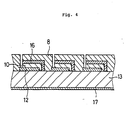
Fig. 4 is a schematic cross section showing an
example of a substrate-integrated type module.
DETAILED DESCRIPTION OF THE INVENTION
The dye-sensitized photoelectric conversion device
according to the present invention comprises an electrically
conductive substrate, a dye-sensitized semiconductor layer
(photosensitive layer) provided on the conductive substrate,
a charge transporting layer, and a counter electrode. The
conductive substrate having the semiconductor layer functions
as a work electrode. The photo-electrochemical cell
according to the invention is a practical application of the
photoelectric conversion device for use as a battery working
in an external circuit.
The photosensitive layer is designed to fit for the
end use and can have either a single layer structure or a
multilayer structure. Light having entered the photosensitive
layer excites the dye. The excited dye has high energy
electrons, which are handed over from the dye to the
conduction band of the semiconductor particles and diffused
to reach the conductive substrate. Meanwhile the dye
molecules are converted into an oxidized state. In a photo-electrochemical
cell, the electrons on the conductive
substrate return to the oxidized dye through the counter
electrode and the charge transporting layer thereby to
regenerate the dye while working in the external circuit.
The semiconductor film acts as a negative electrode of the
cell. The characteristic of the present invention lies in
that the semiconductor layer has two or more different dyes
adsorbed therein. The components of the individual layers
constituting the device may be diffused and mixed mutually at
their boundaries, for example, the boundary between the
conductor layer (hereinafter described) of the conductive
substrate and the photosensitive layer, the boundary between
the photosensitive layer and the charge transporting layer,
and the boundary between the charge transporting layer and
the counter electrode.
The semiconductor serves as a photoreceptor that
absorbs light and separates a charge to generate electrons
and positive holes. In the dye-sensitized semiconductor, the
task of light absorption and generation of electrons and
positive holes is chiefly performed by the dyes, and the
semiconductor plays a role in accepting and transmitting the
electrons.
Examples of the semiconductor which can be used in
the present invention includes single body semiconductors,
e.g., Si or Ge, compound semiconductors, such as metal
chalcogenides (e.g., oxides, sulfides, and selenides), and
perovskite semiconductors. Examples of the metal
chalcogenides include an oxide of titanium, tin, zinc, iron,
tungsten, zirconium, hafnium, strontium, indium, cerium,
yttrium, lanthanum, vanadium, niobium or tantalum; a sulfide
of cadmium, zinc, lead, silver, antimony or bismuth; a
selenide of cadmium or lead; and cadmium telluride. Examples
of the compound semiconductors include a phosphide of zinc,
gallium, indium or cadmium, gallium arsenide, copper-indium-selenide,
and copper-indium-sulfide. Examples of the
perovskite semiconductors include strontium titanate, calcium
titanate, sodium titanate, barium titanate, and potassium
niobate.
Examples of the preferred semiconductors for use in
the invention include Si, TiO2, SnO2, Fe2O3, WO3, ZnO, Nb2O5,
CdS, ZnS, PbS, Bi2S3, CdSe, CdTe, GaP, InP, GaAs, CuInS2, and
CuInSe2. Still preferred are TiO2, ZnO, SnO2, Fe2O3, WO3, Nb2O5,
CdS, PbS, CdSe, InP, GaAs, CuInS2, and CuInSe2. TiO2 is the
most preferred.
The semiconductor may be a single crystal or
polycrystalline. A single crystal is preferred for
conversion efficiency, while a polycrystalline semiconductor
is preferred from the standpoint of production cost, supply
of raw materials, and an energy payback time. Finely
particulate semiconductors having a particle size on the
order of nanometers to microns are particularly preferred.
The particulate semiconductors preferably have an average
primary particle size of 5 to 200 nm, particularly 8 to
100 nm, in terms of a projected area diameter (i.e., an
equivalent circle diameter). The semiconductor particles in
a dispersed state (secondary particles) preferably have an
average particle size of 0.01 to 100 µm.
Semiconductor particles of two or more kinds having
different sizes can be used as a mixture. In this case, the
average size of smaller particles is preferably 5 nm or less.
For the purpose of scattering incident light to improve the
rate of capturing light, large semiconductor particles of
about 300 nm in size may be used in combination.
The particulate semiconductor is preferably prepared
by a sol-gel process described, e.g., in Sumio Sakubana, Sol-gel-ho
no kagaku, Agune Syofusha (1988) and Gijutsu Joho
Kyokai, Sol-gel-ho niyoru hakumaku coating gijutsu (1995),
and a gel-sol process described in Tadao Sugimoto, Materia,
vol. 35, No. 9, pp. 1012-1018, "Shin goseiho gel-sol-ho
niyoru tanbunsan ryushi no gosei to size keitai seigyo"
(1996). The process for preparing an oxide developed by
Degussa AG which comprises pyrogenically hydrolyzing a metal
chloride in an oxyhydrogen flame is also preferred.
For preparation of titanium oxide particles, a
sulfuric acid process and a chlorine process described in
Manabu Seino, Sanka titan busseito ohyogijutu, Gihodo (1997)
are also employable for preference in addition to the above-described
sol-gel process, gel-sol process and pyrogenic
flame hydrolysis.
Of the sol-gel processes for preparing titanium oxide
particles, particularly preferred are the process described
in Barbe, et al., Journal of Americal Ceramic Society, vol.
80, No. 12, pp. 3157-3171 (1997) and the process described in
Burnside et al., Chemistry of Materials, vol. 10, No. 9, pp.
2419-2425.
Examples of the electrically conductive substrate
includes a substrate made of a conductive material, such as
metal, and a substrate made of glass or plastics having on
the surface thereof a conductor layer (i.e., a conductive
layer). Examples of preferred conductors for use in the
latter type of conductive substrates include metals (e.g.,
platinum, gold, silver, copper, aluminum, rhodium, and
indium), carbon, and electrically conductive metal oxides
(e.g., indium tin composite oxide and F-doped tin oxide).
The conductor layer preferably has a thickness of about 0.02
to 10 µm.
The conductive substrate preferably has as low a
surface resistivity as possible. A desirable surface
resistivity is 100 Ω/□(square) or smaller, particularly
40 Ω/□(square) or smaller. While not limiting, the practical
minimal surface resistivity is about 0.1 Ω/□.
It is preferred that the conductive substrate be
substantially transparent to light. The term "substantially
transparent" means that the light transmission is at least
10%, preferably 50% or more, still preferably 70% or more. A
glass or plastic substrate having a conductive metal oxide
layer is preferred as a transparent substrate. Of the above
conductive substrates particularly preferred is conductive
glass obtained by depositing F-doped tin dioxide on
inexpensive soda-lime float glass. For the manufacture of
inexpensive flexible photoelectric conversion devices or
solar cells, a transparent polymer film having the above-described
conductor layer is conveniently used. Examples of
the useful transparent polymers include tetraacetylcellulose
(TAC), polyethylene terephthalate (PET), polyethylene
naphthalate (PEN), syndiotactic polystyrene (SPS),
polyphenylene sulfide (PPS), polycarbonate (PC), polyacrylate
(PAr), polysulfone (PSF), polyester sulfone (PES), polyetherimide
(PEI), cyclic polyolefins, and brominated phenoxy
resins. The amount of the conductive metal oxide is
preferably 0.01 to 100 g/m2 based on the support. The
transparent conductive substrate is preferably used in such a
manner that incident light enters from the side of the glass
or plastic substrate.
In order to decrease the resistance of the
transparent conductive substrate, it is preferred to use a
metal lead, which is preferably made of aluminum, copper,
silver, gold, platinum, nickel, etc., with an aluminum lead
or a silver lead being particularly preferred. It is
preferred that a metal lead be provided on the transparent
substrate by vapor deposition, sputtering or a like
deposition technique, on which a transparent conductor layer
of F-doped tin oxide or ITO is provided. It is also
preferred that the transparent conductor layer be provided on
the transparent substrate, and then the metal lead can be
formed on the transparent conductor layer. Reduction in
incident light quantity due to the metal lead is usually 1 to
10%, preferably 1 to 5%.
The semiconductor particles are applied to the
conductive substrate by, for example, a method comprising
coating on the conductive substrate with a dispersion or
colloidal solution of the particulate semiconductor particles
or the aforementioned sol-gel process, and the like. Film
formation in a wet system is relatively advantageous, taking
into consideration suitability to mass production of a
photoelectric conversion device, liquid physical properties,
and adaptability to various substrates. Film formation in a
wet system is typically carried out by coating or printing.
A dispersion of the semiconductor particles is
prepared by the above-mentioned sol-gel process, a method
comprising grinding a semiconductor in a mortar, or a method
comprising wet grinding a semiconductor in a mill. A
synthetic semiconductor as precipitated in a solvent in the
form of fine particles can also be used as such. Examples of
useful dispersing media include water and various organic
solvents, such as methanol, ethanol, isopropyl alcohol,
dichloromethane, acetone, acetonitrile, and ethyl acetate.
In preparing a dispersion, a polymer, a surface active agent,
an acid, a chelating agent, and the like may be added as a
dispersing aid if desired.
Example of the wet coating techniques include
application methods such as roll coating and dip coating,
metering methods such as air knife coating or blade coating,
and application methods combined with metering such as wire
bar coating (JP-B-58-4589), slide hopper coating (U.S.
Patents 2,681,294, 2,761,419, and 2,761,791), extrusion
coating, and curtain coating. General-purpose spin coating or
spraying techniques are also suitable. Examples of the wet
printing techniques include letterpress printing, offset
printing, gravure printing, intaglio printing, rubber plate
printing, and screen printing. A suitable film formation
system is chosen from among the above-enumerated techniques
in accordance with the liquid viscosity and a desired wet
thickness.
The liquid viscosity is largely dependent on the kind
and the dispersibility of the semiconductor particles, the
solvent, and additives such as a surface active agent and a
binder. In order to form a uniform film, extrusion coating or
casting is fit for a high viscous liquid (e.g., 0.01 to
500 Poise), while slide hopper coating, wire bar coating or
spin coating is suited for a low viscous liquid (e.g.,
0.1 Poise or lower). A low viscous liquid could be applied by
extrusion coating where it is to be applied to some coating
weight. Screen printing, as is often used in applying a
high-viscosity paste of semiconductor particles, can be used
as well. Thus, a suitable wet process for film formation can
be selected in accordance with such parameters as the liquid
viscosity, the coating weight, the type of the substrate, the
speed of application, and so forth.
The semiconductor layer does not need to be a single
layer. Two or more layers different in particle size of
semiconductor particles, in kind of semiconductors or in
composition as for the binder or additives can be provided.
In case where single operation of application is
insufficient for giving a desired thickness, multilayer
coating is effective. Extrusion coating or slide hopper
coating is fit for multilayer coating. Multilayer coating
can be carried out simultaneously or by successively
repeating coating operation several times or more than ten
times. Screen printing is preferably applicable to
successive multilayer coating.
In general, as the thickness of the particulate
semiconductor layer increases, the amount of the dye held per
unit projected area increases to show an increased rate of
capturing light, but the distance of diffusion of generated
electrons also increases, which results in an increased loss
due to re-coupling of charges. Accordingly, there is a
favorable thickness range for the particulate semiconductor
layer, which is typically from 0.1 to 100 µm. Where the
device is used as a photo-electrochemical cell, a more
favorable thickness is 1 to 30 µm, particularly 2 to 25 µm.
The coating weight of the semiconductor particles is
preferably 0.5 to 400 g/m2, still preferably 5 to 100 g/m2.
It is preferred that the semiconductor particles
applied to the substrate be heated to bring them into
electronic contact with each other, to improve film strength,
and to improve adhesion to the substrate. A preferred
heating temperature is 40°C or higher and lower than 700°C,
particularly from 100 to 600°C. The heating time is usually
from 10 minutes to about 10 hours. Where a substrate having
a low melting point or a softening point, such as a polymer
film, is used, high-temperature treatment which would
deteriorate the substrate should be avoided. For the
economical consideration, too, the heating temperature is
preferably as low as possible. The heating temperature can
be lowered by using the above-mentioned small semiconductor
particles having a diameter of up to 5 nm in combination or
by conducting the heat treatment in the presence of a mineral
acid.
For the purpose of increasing the surface area of the
semiconductor particles and of increasing the purity in the
vicinities of the semiconductor particles thereby to improve
electron injection efficiency from the dye to the
semiconductor particles, the heat-treated particulate semi-conductor
layer can be subjected to chemical plating with a
titanium tetrachloride aqueous solution or electro-chemical
plating with a titanium trichloride aqueous solution.
It is preferable for the semiconductor particles to
have a large surface area so that they may adsorb as large an
amount of a dye as possible. The surface area of the
semiconductor particles in the state applied to the
conductive substrate is preferably 10 times or more, still
preferably 100 times or more, the projected area. The
practical upper limit of the surface area is, while not
limited, about 1000 times the projected area.
Examples of the dyes which can be used in the present
invention preferably include metal complex dyes and methine
dyes. In the invention, two or more kinds of dyes are used in
combination so as to broaden the wavelength region of
photoelectric conversion and to increase the conversion
efficiency. The dyes to be combined can be selected in
conformity with the wavelength region of a light source to be
used. It is preferred for the dyes to have an appropriate
interlocking group for linking to the surface of the
semiconductor particles. Examples of preferred inter-locking
groups include -COOH, -SO3H, a cyano group, -P(O)(OH)2,
-OP(O)(OH)2, and chelating groups having pi
conductivity such as oxime, dioxime, hydroxyquinoline,
salicylate and α-keto-enolate groups. Particularly preferred
of them are -COOH, -P(O)(OH)2, and -OP(O)(OH)2. The
interlocking group may be in the form of a salt with an
alkali metal, etc. or an intramolecular salt. Where the
methine chain of a polymethine dye has an acidic group as in
the case where the methine chain forms a squarylium ring or a
croconium ring, that moiety can be used as a interlocking
group.
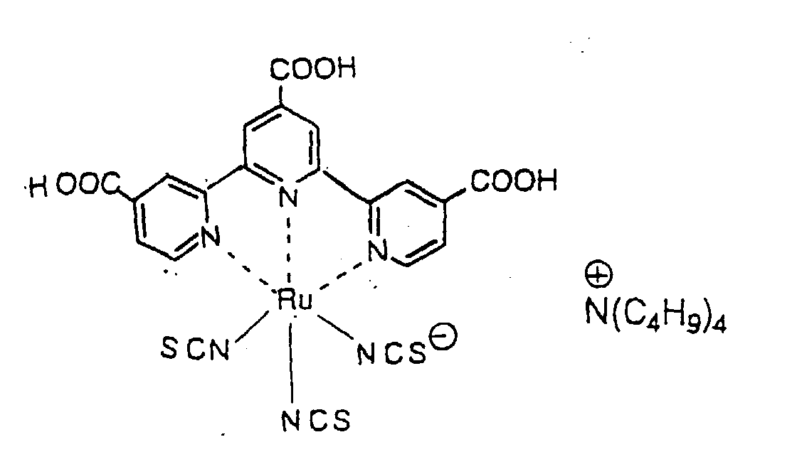
As the metal complex dyes which can be preferably
used in the present invention, ruthenium complex dyes are
preferred. Those represented by formula (I) are still
preferred.
(A1)pRuBaBbBc
wherein A
1 represents a ligand selected from the group
consisting of Cl, SCN, H
2O, Br, I, CN, -NCO and SeCN; p
represents an integer of 0 to 3, preferably 2; and B
a, B
b,
and B
c each represent an organic ligand selected from B-1 to
B-8 shown below.
wherein R
a represents a hydrogen atom, a halogen atom, a
substituted or unsubstituted alkyl group having 1 to 12
carbon atoms, a substituted or unsubstituted aralkyl group
having 7 to 12 carbon atoms, a substituted or unsubstituted
aryl group having 6 to 12 carbon atoms or the interlocking
groups described above. The alkyl group and the alkyl moiety
of the aralkyl group may be either straight or branched, and
the aryl group and the aryl moiety of the aralkyl group may
be either monocyclic or polycyclic (condensed rings).
Examples of useful ruthenium complex dyes are given
in U.S. Patents 4,927,721, 4,684,537, 5,084,365, 5,350,644,
5,463,057, and 5,525,440 and JP-A-7-249790. Specific
examples of preferred ruthenium complex dyes represented by
formula (I) are tabulated below.
| (A1)pRuBaBbBc |
| No. | A1 | P | Ba | Bb | Bc | Ra |
| R-1 | SCN | 2 | B-1 | B-1 | - | - |
| R-2 | CN | 2 | B-1 | B-1 | - | - |
| R-3 | Cl | 2 | B-1 | B-1 | - | - |
| R-4 | Br | 2 | B-1 | B-1 | - | - |
| R-5 | I | 2 | B-1 | B-1 | - | - |
| R-6 | SCN | 2 | B-1 | B-2 | - | H |
| R-7 | SCN | 1 | B-1 | B-3 | - | - |
| R-8 | Cl | 1 | B-1 | B-4 | - | H |
| R-9 | I | 2 | B-1 | B-5 | - | H |
| R-10 | SCN | 2 | B-1 | B-6 | - | H |
| R-11 | CN | 2 | B-1 | B-7 | - | H |
| R-12 | Cl | 1 | B-1 | B-8 | - | H |
| R-13 | - | 0 | B-1 | B-1 | B-1 | - |
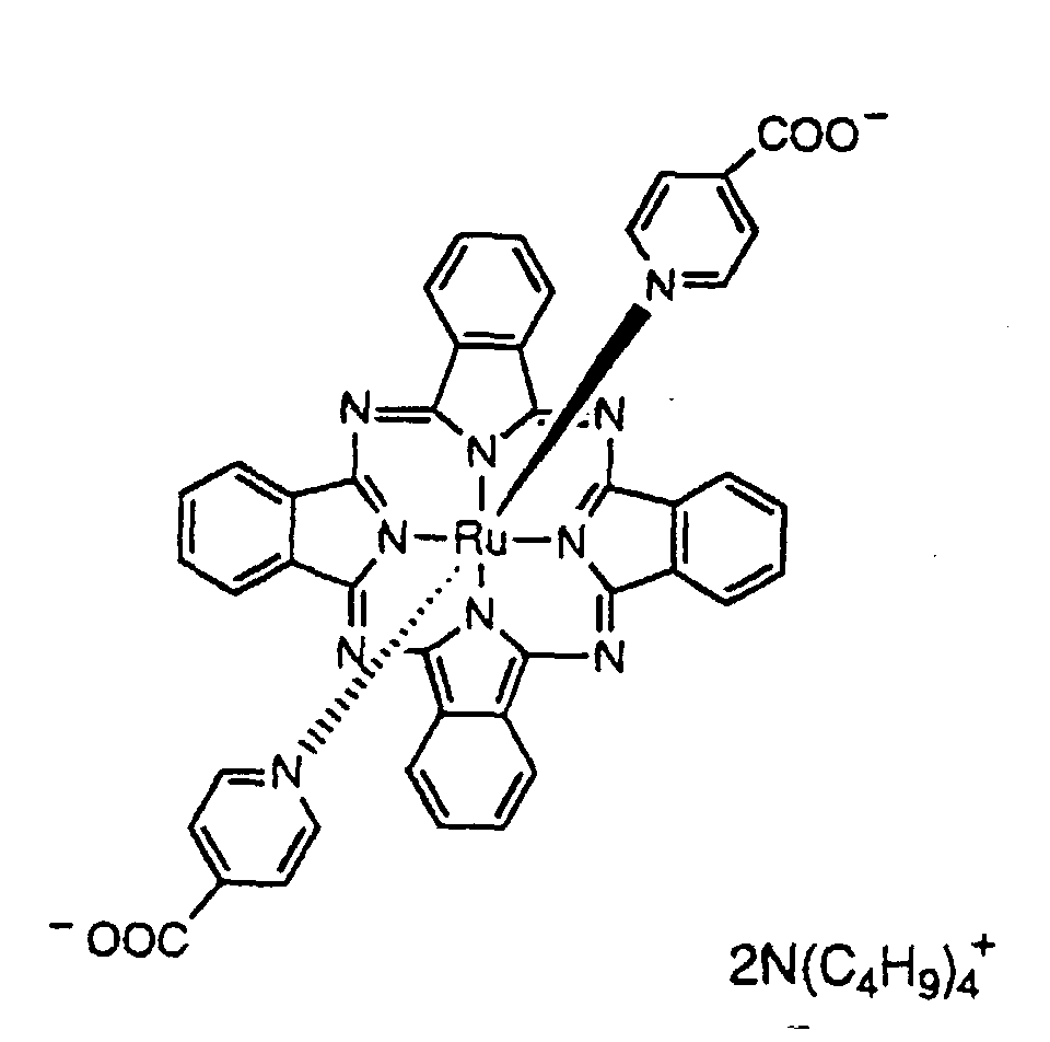
Specific examples of other suitable metal complex
dyes are shown below. Also, Dyes E, H, K and L used in the
examples hereafter given are included in preferred examples.
The polymethine dyes preferably include those
represented by formulae (II), (III), (IV) or (V) shown below.
wherein R
b and R
f each represent a hydrogen atom, an alkyl
group, an aryl group or a heterocyclic group; R
c, R
d, and R
e
each represent a hydrogen atom or a substituent; R
b, R
c, R
d,
R
e, and R
f may be bonded each other to form a ring; X
11 and X
12
each represent a nitrogen atom, an oxygen atom, a sulfur atom,
a selenium atom or a tellurium atom; n11 and n13 each
represent an integer of 0 to 2; and n12 represents an integer
of 1 to 6.
The compound of formula (II) may have a counter ion
in agreement with the charge quantity of the whole molecule.
In formula (II), the alkyl, aryl, and heterocyclic groups may
have a substituent; the alkyl group may be straight or
branched; the aryl and heterocyclic groups may be monocyclic
or polycyclic (condensed rings); and the ring formed of R
b,
R
c, R
d, R
e, and R
f may have a substituent and may be
monocyclic or polycyclic.
wherein Z
a represents a non-metallic atom group necessary to
form a nitrogen-containing heterocyclic ring; R
g represents
an alkyl group or an aryl group; Q
a represents a mono- or
polymethine group necessary to complete a (poly)methine dye;
X
13 represents a counter ion in balance; and n14 represents a
number of from 0 up to 10 that is necessary to neutralize the
charge of the molecule.
In formula (III), the nitrogen-containing
heterocyclic ring formed by Za may have a substituent and may
be a single ring or a condensed ring; the alkyl or aryl
groups may have a substituent; the alkyl group may be
straight or branched; and the aryl group may be monocyclic or
polycyclic (condensed rings).
The dyes represented by formula (III) preferably
include those represented by formulae (III-a) through (III-d):
wherein R
11, R
12, R
13, R
14, R
15, R
21, R
22, R
23, R
24, R
31, R
32, R
33,
R
41, R
42, and R
43 each represent a hydrogen atom, an alkyl
group, an aryl group or a heterocyclic group; Y
11, Y
12, Y
21, Y
22,
Y
31, Y
32, Y
33, Y
34, Y
35, Y
41, Y
42, Y
43, Y
44, Y
45, and Y
46 each
represent an oxygen atom, a sulfur atom, a selenium atom, a
tellurium atom, -CR
16R
17- or -NR
18-; R
16, R
17, and R
18 each
represent a hydrogen atom, an alkyl group, an aryl group or a
heterocyclic group; Y
23 represents O
-, S
-, Se
-, Te
- or -NR
18 -;
V
11, V
12, V
21, V
22, V
31, and V
41 each represent a substituent;
and n15, n31, and n41 each represent an integer of 1 to 6.
The compounds represented by formulae (III-a) to
(III-d) may have a counter ion in agreement with the charge
quantity of the whole molecule. In these formulae, the alkyl,
aryl, and heterocyclic groups may have a substituent; the
alkyl group may be straight or branched; and the aryl or
heterocyclic group may be monocyclic or polycyclic (condensed
rings).
Examples of the above-described polymethine dyes are
found in M. Okawara, T. Kitao, T. Hirashima, and M. Matuoka,
Organic Colorants, Elsevier.
wherein Q
b represents an atom group necessary to complete a
5- or 6-membered nitrogen-containing heterocyclic ring which
may be a condensed ring and may have a substituent; Z
b
represents an atom group necessary to complete a 3- to 9-membered
ring, the atom group being composed of atoms
selected from carbon, oxygen, nitrogen, sulfur, and hydrogen;
L
1, L
2, L
3, L
4, and L
5 each represent a substituted or
unsubstituted methine group; n
51 represents an integer of 0
to 4; n
52 represents 0 or 1; R
5 represents a substituent; and
W
1 represents a counter ion necessary to neutralize the
charge quantity.
In formula (IV), examples of the 5- or 6-membered
heterocyclic ring completed by Qb preferably includes
benzothiazole, benzoxazole, benzoselenazole, benzotellurazole,
2-quinoline, 4-quinoline, benzimidazole, thiazoline,
indolenine, oxadiazole, thiazole, and imidazole nuclei.
Preferred of them are benzothiazole, benzoxazole,
benzimidazole, benzoselenazole, 2-quinoline, 4-quinoline, and
indolenine nuclei. Particularly preferred of them are
benzothiazole, benzoxazole, 2-quinoline, 4-quinoline, and
indolenine nuclei. Examples of the substituent that can be
on the ring includes a carboxyl group, a phosphonic acid
group, a sulfonic acid group, a halogen atom (i.e., F, Cl, Br
or I), a cyano group, an alkoxy group (e.g., methoxy, ethoxy
or methoxyethoxy), an aryloxy group (e.g., phenoxy), an alkyl
group (e.g., methyl, ethyl, cyclopropyl, cyclohexyl,
trifluoromethyl, methoxyethyl, allyl or benzyl), an alkylthio
group (e.g., methylthio or ethylthio), an alkenyl group (e.g.,
vinyl or 1-propenyl), and an aryl or heterocyclic group (e.g.,
phenyl, thienyl, toluoyl or chlorophenyl).
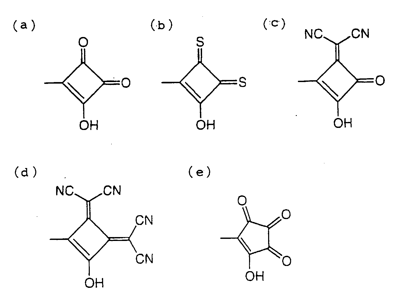
The 3- to 9-membered ring completed by Z
b preferably
has a skeleton made up of 4 to 6 carbon atoms. Preferred
rings completed by Z
b are shown below. Ring (a) is the most
desirable.
Examples of the substituents that may be on the
methine groups L1, L2, L3, L4, and L5 include a substituted or
unsubstituted alkyl group (preferably an alkyl group having 1
to 12, particularly 1 to 7, carbon atoms, such as methyl,
ethyl, propyl, isopropyl, cyclopropyl, butyl, 2-carboxyethyl
or benzyl), a substituted or unsubstituted aryl group
(preferably an aryl group having 6 to 10 carbon atom,
particularly 6 to 8 carbon atoms, such as phenyl, toluoyl,
chlorophenyl or o-carboxyphenyl), a heterocyclic group (e.g.,
pyridyl, thienyl, furanyl, pyridyl or barbituric acid), a
halogen atom (e.g., chlorine or bromine), an alkoxy group
(e.g., methoxy or ethoxy), an amino group (preferably an
amino group having 1 to 12, particularly 6 to 12, carbon
atoms, e.g., diphenylamino, methylphenylamino or 4-acetylpiperazin-1-yl),
and an oxo group. The substituents on
the methine group may be connected to each other to form such
a ring as a cyclopentene ring, a cyclohexene ring or a
squarylium ring. The substituent can form a ring together
with an auxochrome.
n51 preferably represents an integer of from 0 to 3.
R5 preferably represents a substituted or
unsubstituted aromatic group or a substituted or
unsubstituted aliphatic group. The aromatic group preferably
has 5 to 16, particularly 5 or 6, carbon atoms, and the
aliphatic group preferably has 1 to 10, particularly 1 to 6,
carbon atoms. Examples of the aliphatic and aromatic groups
as unsubstituted include methyl, ethyl, n-propyl, n-butyl,
phenyl, and naphthyl groups.
W1 represents a counter ion necessary to neutralize
the charge quantity. Whether a dye is cationic or anionic or
whether or not it has a net ionic charge depends on its
auxochrome and substituent. Where a dye carries a
dissociating group, it can dissociate to possess a negative
charge. In this case, too, the total amount of charges is
neutralized with W1. Typical cations include inorganic or
organic ammonium ions (e.g., tetraalkylammonium ion and
pyridinium ion) and alkali metal ions. Typical anions, which
may be either organic or inorganic, include halide ions (e.g.,
fluoride, chloride, bromide or iodide ions), substituted
arylsulfonate ions (e.g., p-toluenesulfonate ion or p-chlorobenzenesulfonate
ion), aryldisulfonate ions (e.g., 1,3-benzenedisulfonate
ion, 1,5-naphthalenedisulfonate ion, and
2,6-naphthalenedisulfonate ion), alkylsulfate ions (e.g.,
methylsulfate ion), a sulfate ion, a thiocyanate ion, a
perchlorate ion, a tetrafluoroborate ion, a picrate ion, an
acetate ion, and a trifluoromethanesulfonate ion.
W
1, as a charge balancing counter ion, could be an
ionic polymer or a dye having an opposite charge. A metal
complex ion (e.g., bisbenzene-1,2-dithiolatonickel (III))
also serves as W
1.
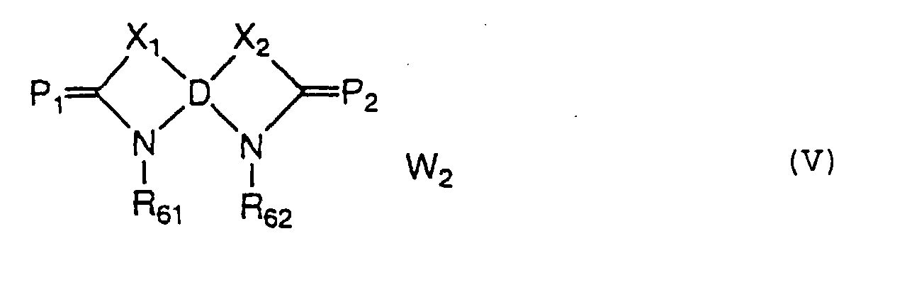
wherein D represents an aromatic group having tetra- or
higher-functionality; X
1 and X
2 each represent a sulfur atom,
a selenium atom, CR
63R
64 or CR
65=CR
66, wherein R
63, R
64, R
65, and
R
66 each represent a hydrogen atom or an alkyl group; R
61 and
R
62 each represent an aliphatic group or an aromatic group; P
1
and P
2 each represent a non-metallic atom group necessary to
complete a polymethine dye; and W
2 represents a counter ion
necessary to neutralize the charge of the whole molecule.
In formula (V), examples of the aromatic group having
tetra- or higher-functionality represented by D includes
those derived from aromatic hydrocarbons such as benzene,
naphthalene, anthracene, and phenanthrene; and aromatic
heterocyclic compounds such as anthraquinone, carbazole,
pyridine, quinoline, thiophene, furan, xanthene, and
thianthrene. The group D may have a substituent on a
position other than the linking positions. D is preferably a
group derived from an aromatic hydrocarbon, particularly
benzene or naphthalene.
X1 and X2 each preferably represent a sulfur atom or
CR63R64, particularly CR63R64.
While the methine dye represented by formula (V)
embraces various kinds according to P1 and P2, examples of
the typical methine dye includes cyanine dyes, merocyanine
dyes, rhodacyanine dyes, trinuclear merocyanine dyes,
holopolar dyes, hemicyanine dyes, and styryl dyes. The
cyanine dyes include those in which the substituents on the
methine chain form a squarylium ring or a croconium ring.
For the details of these dyes, reference can be made in F.M.
Harmer, Heterocyclic Compounds-Cyanine Dyes and Related
Compounds, John Wiley & Sons (1964) and D.M. Sturmer,
Heterocyclic Compounds-Special Topics in Heterocyclic
Chemistry, ch. 18, §14, pp. 482-515, John Wiley & Sons (1977).
The cyanine dyes, merocyanine dyes, and rhodacyanine dyes
described in U.S. Patent 5,340,694 with the respective
formulae (XI), (XII), and (XIII) are preferred. It is
preferred for at least one, desirably both, of the methine
chains contained in P1 and P2 to have a squarylium ring.
R61 and R62 each represent a substituted or
unsubstituted aromatic group or a substituted or
unsubstituted aliphatic group. The aromatic group preferably
has 5 to 16, particularly 5 or 6, carbon atoms, and the
aliphatic group preferably has 1 to 10, particularly 1 to 6,
carbon atoms. Examples of the aliphatic and aromatic groups
as unsubstituted include methyl, ethyl, n-propyl, n-butyl,
phenyl, and naphthyl groups.
The compound of formula (V) preferably carries an
acidic group in at least one of R61, R62, P1, and P2. The term
"acidic group" means a substituent having a dissociating
proton and includes a group derived from carboxylic acid,
phosphonic acid, sulfonic acid, boric acid, etc., with a
carboxyl group being preferred. The acidic group may release
the proton to take a dissociated form.
W2 has the same meaning as W1 in formula (IV).
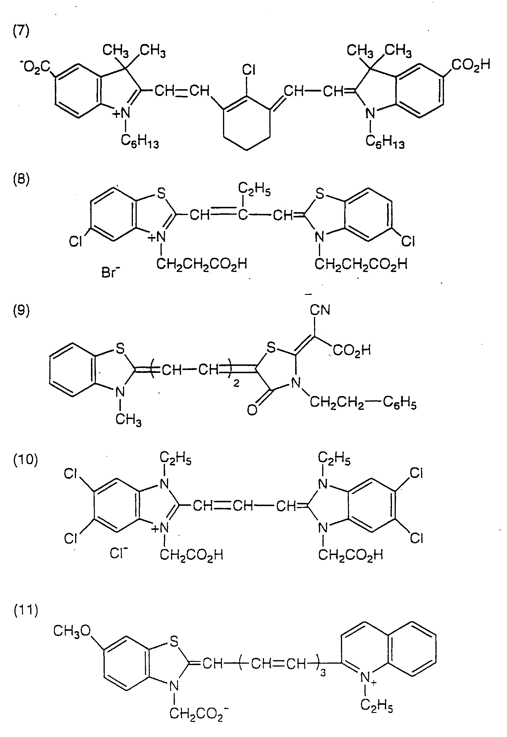
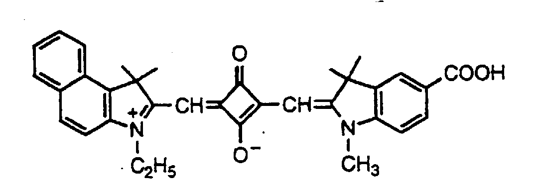
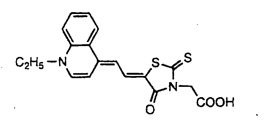
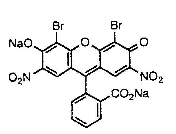
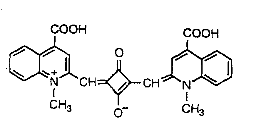
Specific and preferred examples of the polymethine
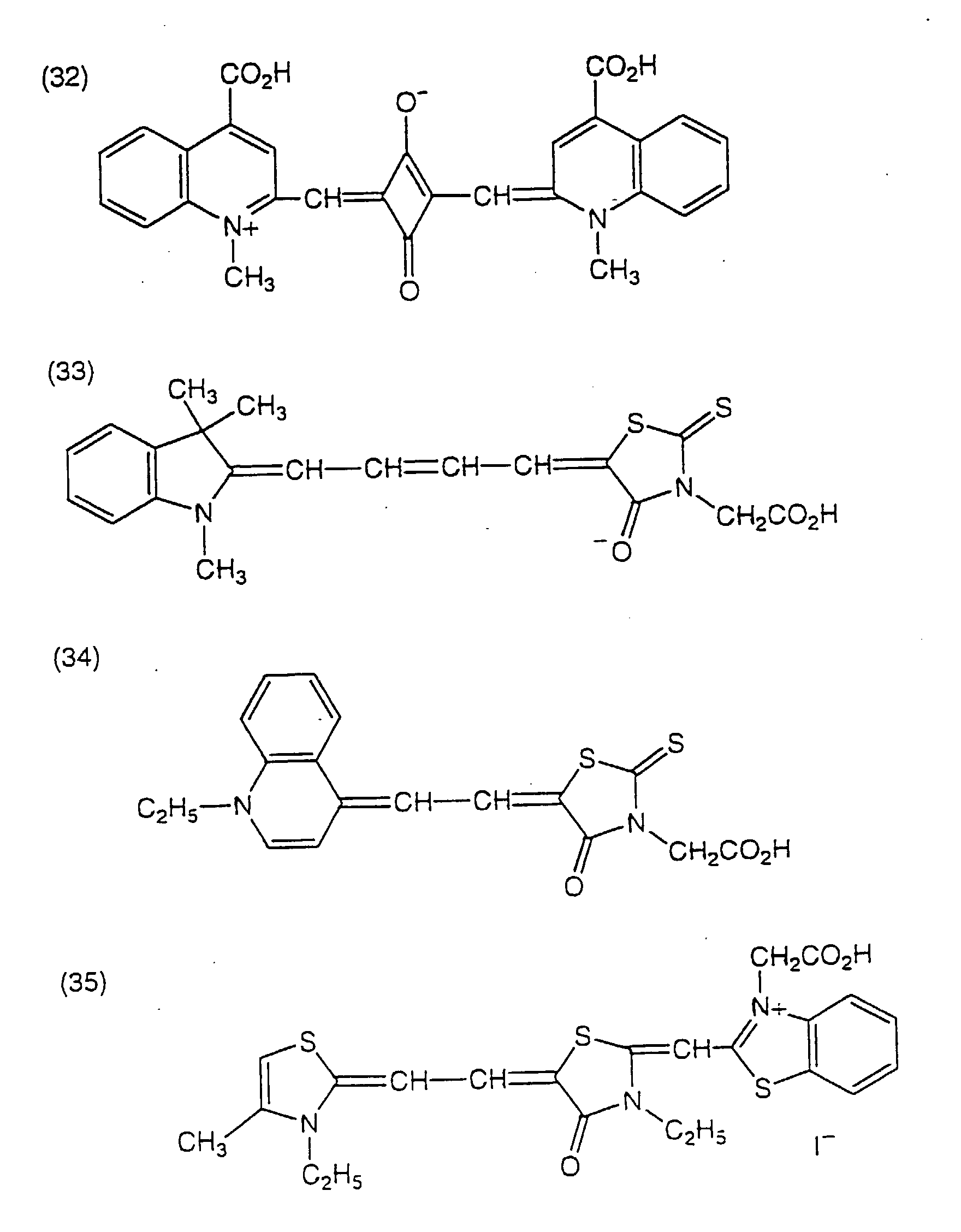
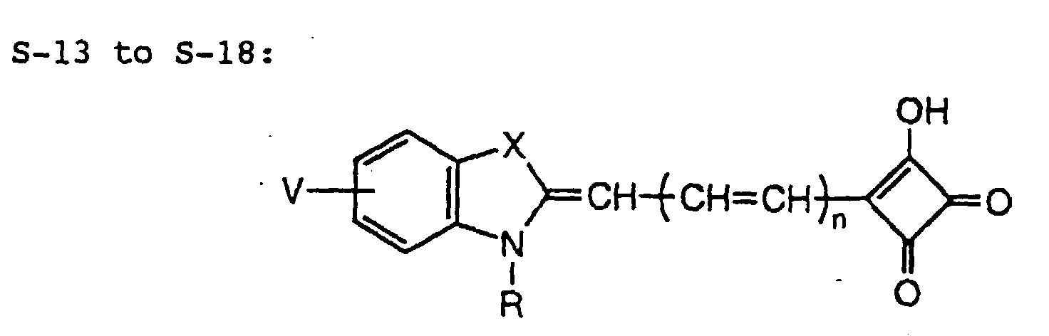
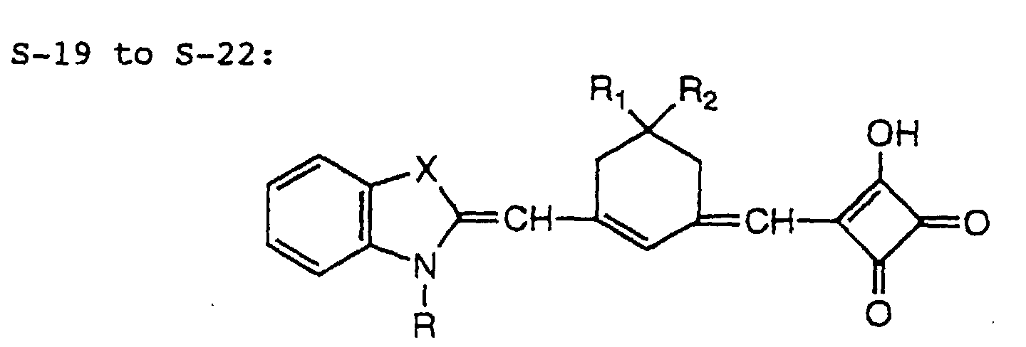
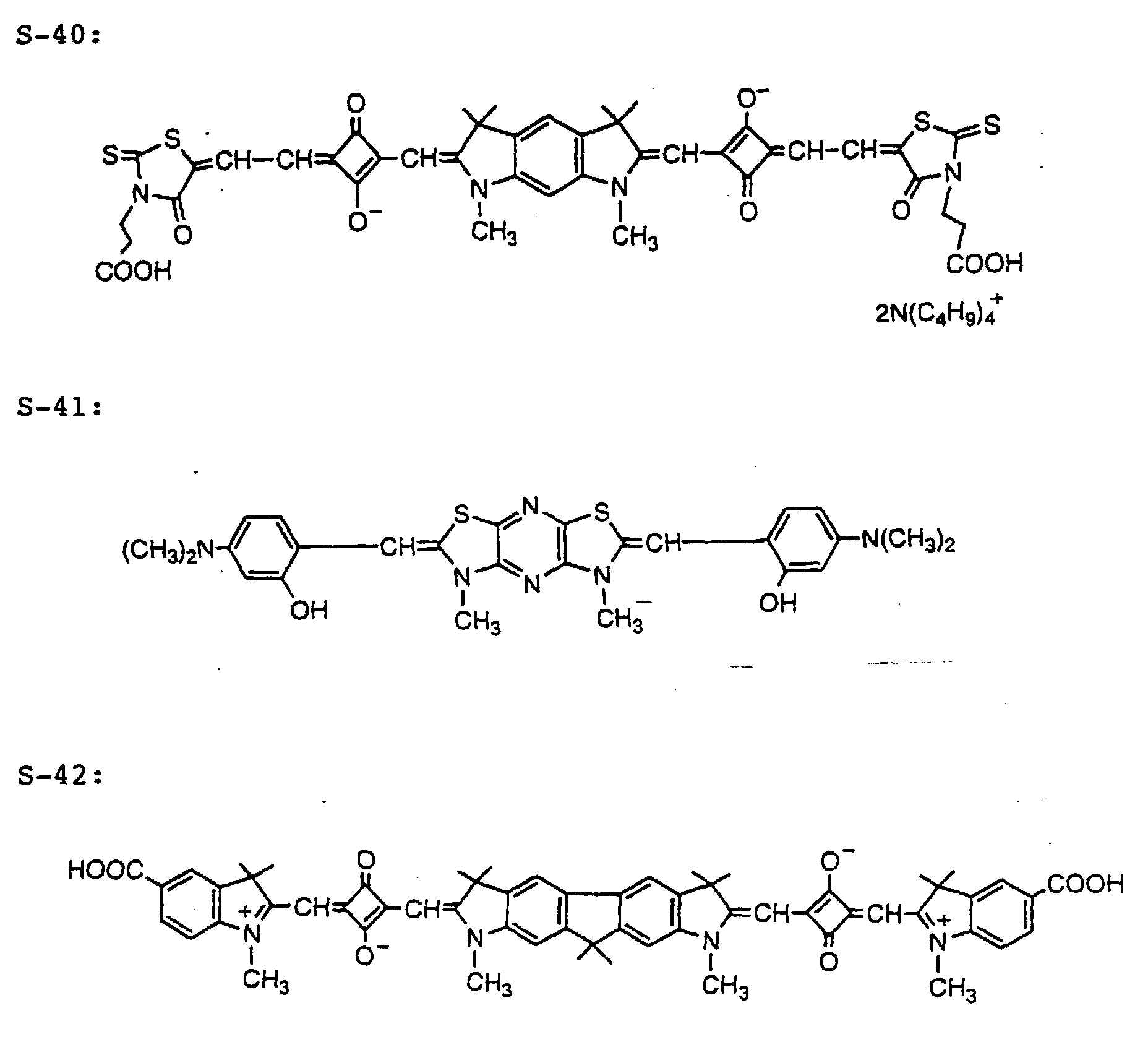
dyes represented by formulae (II) to (V) are shown below.
Dyes B, D, F, G, and I used in the examples hereinafter given
are also included in preferred examples.
| Compound No. | X | V | R | Y1 | Y2 |
| S-1 | C(CH3)2 | 4,5-benzo | C3H7 | O | O |
| S-2 | C(CH3)2 | H | (CH3)2COOH | O | O |
| S-3 | C(CH3)2 | 4,5-benzo | C2H5 | S | S |
| S-4 | C(CH3)2 | 4,5-benzo | C2H5 | C(CN)2 | O |
| S-5 | C(CH3)2 | 4,5-benzo | C2H5 | C(CN)2 | C(CN)2 |
| S-6 | S | H | C2H5 | O | O |
| S-7 | S | 5,6-benzo | CH3 | O | O |
| S-8 | O | H | CH3 | O | O |
| S-9 | Se | H | CH3 | O | O |
| S-10 | NC2H5 | H | CH3 | O | O |
| S-11 | -CH=CH- | H | C2H5 | O | O |
| Compound No. | X | V | R | n |
| S-13 | C(CH3)2 | H | CH3 | 1 |
| S-14 | C(CH3)2 | 4,5-benzo | C2H5 | 1 |
| S-15 | S | H | CH3 | 2 |
| S-16 | S | 5,6-benzo | C2H5 | 3 |
| S-17 | S | 5,6-benzo | C2H5 | 4 |
| S-18 | O | H | CH | 3 | 4 |
| Compound No. | X | R1 | R2 | R |
| S-19 | C(CH3)2 | CH3 | CH3 | C2H5 |
| S-20 | S | CH3 | CH3 | C2H5 |
| S-21 | O | CH3 | CH3 | (CH2)3COOH |
| S-22 | O | Ph | H | C2H5 |
| Compound No. | X | Y | R1 | R2 | V1 | W |
| S-23 | S | S | CH3 | CH3 | H | I_ |
| S-24 | S | S | C2H5 | CH3 | 5-COOH | I_ |
| S-25 | C(CH3)2 | C(CH3)2 | CH3 | CH3 | 5-COOH | I_ |
| S-26 | C(CH3)2 | C(CH3)2 | CH2CH2COOH | C2H5 | H | Cl- |
| S-27 | O | C(CH3)2 | CH3 | C2H5 | H | I- |
| Compound No. | X | Y | R1 | R2 | V1 |
| S-28 | S | C(CH3)2 | CH3 | CH3 | H |
| S-29 | S | C(CH3)2 | C3H7 | CH3 | 4,5-benzo |
| S-30 | C(CH3)2 | S | CH3 | CH3 | 5-COOH |
| S-31 | C(CH3)2 | C(CH3)2 | CH3 | CH3 | 5-COOH |
| S-32 | C(CH3)2 | NCH3 | CH3 | C2H5 | 5-CH3 |
| Compound No. | X | Y | R1 | R2 | V1 |
| S-33 | S | C(CH3)2 | CH3 | CH3 | H |
| S-34 | S | C(CH3)2 | C2H5 | CH3 | 5-SO3H |
| S-35 | C(CH3)2 | C(CH3)2 | CH3 | CH2H5 | 5-COOH |
| S-36 | C(CH3)2 | C(CH3)2 | CH2CH2COOH | CH3 | 4,5-benzo |
| S-37 | C(CH3)2 | NCH3 | CH3 | C2H5 | 5-CH3 |
The compounds of formulae (II) and (III) are
synthesized with reference to the teachings of F.M. Harmer,
Heterocyclic Compounds-Cyanine Dyes and Related Compounds,
John Wiley & Sons (1964), D.M. Sturmer, Heterocyclic
Compounds-Special Topics in Heterocyclic Chemistry, ch. 18,
§14, pp. 482-515, John Wiley & Sons (1977), and Rodd's
Chemistry of Carbon Compounds, 2nd Ed., vol. IV, part B, ch.
15, cls. 369-422, Elsevier Science Publishing Company Inc.
(1977), and GB Patent 1,077,611. The compounds of formula
(IV) are synthesized with reference to the disclosure, e.g.,
of Dyes and Pigments, vol. 21, pp. 227-234. The compounds of
formula (V) are synthesized with reference, e.g., to
Ukrainskii Khimicheskii Zhurnal, vol. 40, No. 3, pp. 253-258,
Dyes and Pigments, vol. 21, pp. 227-234, and the literature
cited therein.
Two or more, preferably three or more kinds of dyes
are used in combination so as to broaden the wavelength
region of photoelectric conversion and to increase the
conversion efficiency.
It is a highly preferred embodiment that at least one
of the dyes shows a maximum conversion efficiency for
incident photon to current (i.e., a maximum incident photon
to current conversion efficiency at a wavelength of 300 nm or
longer and shorter than 600 nm (i.e., from 300 nm to 598 nm
or shorter), preferably 450 nm or longer and shorter than
600 nm (i.e., from 450 nm to 598 nm), when adsorbed alone in
the semiconductor-containing layer, and at least another dye
exhibits a maximum incident photon to current conversion
efficiency at a wavelength of 600 to 850 nm when adsorbed
alone in the semiconductor layer. The incident photon to
current conversion efficiency (hereinafter abbreviated as
IPCE), which is a parameter indicative of photoelectric
conversion ability, is a value obtained by dividing the
number of photoelectrons generated on irradiation with light
having a certain wavelength or a certain range of wavelengths
by the number of incident photons. More specifically, IPCE
is (number of photons absorbed by a dye) × (quantum
efficiency in electron injection from dye to
semiconductor)/(number of incident photons) × 100 (unit: %).
Dyes having a maximum IPCE at 300 nm or longer and
shorter than 600 nm are preferably selected from the
ruthenium complex dyes represented by formula (I) and the
polymethine dyes represented by formulae (II), (III), (IV)
and (V). The ruthenium complex dyes and the polymethine dyes
of formula (III-b) or (IV) which have a partial structure
derived from a squaric acid are still preferred. Dyes having
a maximum IPCE at 600 to 850 nm are preferably selected from
the ruthenium complex dyes represented by formula (I) and the
polymethine dyes of formulae (II), (III), (IV) or (V), still
preferably the ruthenium complex dyes, the polymethine dyes
of formula (III-b) or the polymethine dyes of formula (IV) or
(V) which have a partial structure derived from a squaric
acid.
Where three or more dyes are to be adsorbed, it is
desirable that at least one of the dyes has a maximum IPCE at
300 nm or longer and shorter than 550 nm (i.e., 300 to
548 nm) when adsorbed alone, at least another dye has a
maximum IPCE at 550 nm or longer and shorter than 700 nm
(i.e., 550 to 698 nm) when adsorbed alone, and at least still
another dye has a maximum IPCE at 700 to 850 nm when adsorbed
alone in the semiconductor-containing layer. It is more
desirable that at least one of the dyes has a maximum IPCE at
400 nm or longer and shorter than 550 nm (i.e., 400 to
548 nm), at least another dye has a maximum IPCE at 550 nm or
longer and shorter than 700 nm (i.e., 550 to 698 nm), and at
least still another dye has a maximum IPCE at 700 to 850 nm.
Dyes having a maximum IPCE at 300 nm or longer and
shorter than 550 nm are preferably selected from the
ruthenium complex dyes of formula (I) and the polymethine
dyes of formulae (II), (III), (IV), and (V), still preferably
the ruthenium complex dyes, the polymethine dyes of formula
(III-b), and the polymethine dyes of formula (IV) which have
a partial structure derived from a squaric acid. Dyes having
a maximum IPCE at 550 nm or longer and shorter than 700 nm
are preferably selected from the ruthenium complex dyes of
formula (I) and the polymethine dyes of formulae (II), (III),
(IV), and (V), still preferably the ruthenium complex dyes,
the polymethine dyes of formula (III-b), and the polymethine
dyes of formula (IV) which have a partial structure derived
from a squaric acid. Dyes having a maximum IPCE at 700 to
850 nm are preferably selected from the ruthenium complex
dyes of formula (I) and the polymethine dyes of formulae (II),
(III), (IV), and (V), still preferably the polymethine dyes
of formula (III-b) and the polymethine dyes of formula (IV)
and (V) which have a partial structure derived from a squaric
acid. Of these dyes having a maximum IPCE at 700 to 850 nm,
particularly preferred are bis-type polymethine dyes having
two conjugated methine chains, e.g., the compounds S-28 to S-37
and dye I used in Examples hereinafter given.
A photoelectric conversion device having adsorbed two
or more dyes shows a plurality of peaks of IPCE according to
the dyes used when measured in a wavelength range of 300 to
850 nm. It is preferred that the lowest to highest peak
ratio be 0.05 to 1, particularly 0.1 to 1, especially 0.3 to
1. It is also preferred that the maximum IPCE of a
photoelectric conversion device having adsorbed two or more
dyes be at least 40%, particularly 50% or more, especially
60% or more.
Adsorption of the dye onto semiconductor particles is
usually effected by dipping well-dried work electrode
containing semiconductor particles in a dye solution (e.g.,
immersion, dip coating, roll coating or air knife coating),
coating the semiconductor layer with a dye solution (e.g.,
wire bar coating, slide hopper coating, extrusion coating,
curtain coating, spin coating, spraying), or printing (e.g.,
letterpress printing, offset printing, gravure printing, or
screen printing). All the dyes may be dissolved in the same
solvent to prepare a single dye solution, or a plurality of
dye solutions containing each dye or more than one dye may be
applied successively.
As previously described with regard to the formation
of the particulate semiconductor layer, extrusion coating and
various printing methods are fit for a high viscous liquid
(e.g., 0.01 to 500 Poise), while slide hopper coating, wire
bar coating and spin coating are suited for a low viscous
liquid (e.g., 0.1 Poise or lower) to form a uniform film. In
this way, an appropriate technique for dye adsorption is to
be selected according to such parameters as the viscosity of
the dye solution, the coating weight, the kind of the
substrate, the speed of application, and the like. Taking
the suitability to mass production, the time required for dye
adsorption after dye application is conveniently as short as
possible.
The above-described heat treatment of the
semiconductor layer before dye adsorption is also favorable
for increasing the amount of the dyes adsorbed. In this case,
it is preferred that the dyes be quickly adsorbed into the
heated semiconductor layer while it is between 40°C and 80°C
so as to prevent water from being adsorbed to the
semiconductor particles.
In order to obtain a sufficient sensitizing effect,
the dyes are preferably adsorbed in a total amount of 0.01 to
100 mmol per m2 of the substrate and 0.01 to 1 mmol per gram
of the particulate semiconductor particles. With too small a
total amount of the dyes, the sensitizing effect would be
insufficient. If the dyes are used in too large a total
amount, the non-adsorbed dyes will float only to reduce the
sensitizing effect.
A colorless compound may be adsorbed together with
the dyes so as to lessen the interaction among dye molecules,
such as association. Hydrophobic compounds such as carboxyl
group-containing steroid compounds (e.g., cholic acid) can be
used for this purpose.
Because the dyes remaining unadsorbed causes
disturbances of device performance, they should be washed
away immediately after adsorption. Washing is conveniently
carried out in a wet washing tank with an organic solvent,
such as a polar solvent (e.g., acetonitrile) or an alcohol.
After dye adsorption, the surface of the semiconductor
particles can be treated with an amine to accelerate removal
of the unadsorbed dyes. Examples of preferred amines include
pyridine, 4-t-butylpyridine, and polyvinylpyridine. The
amine can be used as such where it is liquid, or as dissolved
in an organic solvent.
The charge transporting layer is a layer having a
function of replenishing oxidized dyes with electrons. The
charge transporting layer typically includes a solution of a
redox system in an organic solvent (i.e., an electrolytic
solution), a gel electrolyte comprising a polymer matrix
impregnated with a solution of a redox system in an organic
solvent, and a molten salt containing a redox system. A
solid electrolyte or a hole-transporting material can be used
in place of an electrolyte.
An electrolytic solution used in the invention
preferably comprises an electrolyte, a solvent, and additives.
Examples of the electrolyte includes combinations of I2 and
iodides (for example, metal iodides, such as LiI, NaI, KI,
CsI or CaI2, and an iodine salt of quaternary ammonium
compounds, such as a tetraalkylammonium iodide, pyridinium
iodide and imidazolium iodide); combinations of Br2 and
bromides (for example, metal bromides, such as LiBr, NaBr,
KBr, CsBr or CaBr2, and a bromine salt of quaternary ammonium
compounds, such as a tetraalkylammonium bromide or pyridinium
bromide); metal complexes, such as a ferrocyananate-ferricyanate
system or a ferrocene-ferricinium ion system;
sulfur compounds, such as poly(sodium sulfite) and an
alkylthiol-alkyl disulfide; viologen dyes; hydroquinone-quinone;
and the like. Preferred of them are combinations of
I2 and an iodine salt of a quaternary ammonium compound, such
as pyridinium iodide or imidazolium iodide. These
electrolytes can be used either individually or as a mixture
thereof. Molten salts (salts which take a molten state at
roam temperature) described in EP 718288, WO95/18456, J.
Electrochem. Soc., vol. 143, No. 10, p. 3099 (1996),
Electrochemistry, vol. 65, No. 11, p.923, and Inorg. Chem.,
vol. 35, pp. 1168-1178 (1996) are also useful as an
electrolyte. In using a molten salt, a solvent is
unnecessary.
It is preferred that the molten salt (electrolyte)
is used in the charge transporting layer of the
photoelectric conversion device of the present invention.
Examples of the molten salt include a pyridinium
salt, an imidazolium salt and a triazolium salt.
The concentration of the electrolyte is preferably
from 0.1 to 15 M, more preferably from 0.2 to 10 M. Also,
when the iodine is added to the electrolyte, the
concentration of iodine is preferably from 0.01 to 0.5 M.
It is preferred for the solvent dissolving the
electrolyte to have a low viscosity and a high dielectric
constant. To have a low viscosity leads to an improvement
in ion mobility. To have a high dielectric constant brings
about an increase in effective carrier concentration.
Examples of suitable organic solvents include carbonate
compounds, such as ethylene carbonate and propylene
carbonate; heterocyclic compounds, such as 3-methyl-2-oxazolidinone;
ether compounds, such as dioxane and diethyl
ether; acyclic ethers (i.e., chain ethers), such as ethylene
glycol dialkyl ethers, propylene glycol dialkyl ethers,
polyethylene glycol dialkyl ethers, and polypropylene glycol
dialkyl ethers; alcohols, such as methanol, ethanol, ethylene
glycol monoalkyl ethers, propylene glycol monoalkyl ethers,
polyethylene glycol monoalkyl ethers, and polypropylene
glycol monoalkyl ethers; polyhydric alcohols, such as
ethylene glycol, propylene glycol, polyethylene glycol,
polypropylene glycol, and glycerol; nitrile compounds, such
as acetonitrile, glutaronitrile, methoxyacetonitrile,
propionitrile, and benzonitrile; aprotic polar solvents, such
as dimethyl sulfoxide (DMSO) and sulfolane; and water.
The electrolyte can contain a basic compound, such as
tert-butylpyridine, 2-picoline, and 2,6-lutidine, as
disclosed in J. Am. Ceram. Soc., vol. 80, No. 12, pp. 3157-3171
(1997). A preferred concentration of the basic compound
is 0.05 to 2 M.
A liquid electrolyte can be solidified to gel by
addition of a polymer, addition of an oil gelling agent,
polymerization of a polyfunctional monomer, crosslinking of a
polymer, or a like technique. Polymers which can be added to
cause the electrolyte to gel include the compounds described
in J.R. MacCallum and C.A. Vincent, Elsevier Applied Science,
"Polymer Electrolyte Reviews-1 and 2". Polyacrylonitrile and
polyvinylidene fluoride are particularly preferred.
Oil gelling agents include the compounds disclosed in
J. Chem. Soc. Japan, p. 46779, Ind. Chem. Soc. (1943), J. Am.
Chem. Soc., vol. 111, p. 5542 (1989), J. Chem. Soc., Chem.
Commun., p. 390 (1993), Angew. Chem. Int. Ed. Engl., vol. 35,
p. 1949 (1996), Chem. Lett., p. 885 (1996), and J. Chem. Soc.,
Chem. Commun., p. 545 (1997). Preferred of them are those
having an amide structure in the molecule.
Where a gel electrolyte is prepared by polymerization
of a polyfunctional monomer, a preferred process comprises
applying a composition comprising a polyfunctional monomer, a
polymerization initiator, an electrolyte, and a solvent to a
dye-sensitized electrode by casting, coating, dipping,
impregnation or a like technique to form a sol electrolyte
layer, followed by radical polymerization to make the sol
into gel. Preferred polyfunctional monomers are those having
two or more ethylenically unsaturated groups per molecule,
such as divinylbenzene, ethylene glycol dimethacrylate,
ethylene glycol diacrylate, ethylene glycol dimethacrylate,
diethylene glycol diacrylate, diethylene glycol
dimethacrylate, triethylene glycol diacrylate, triethylene
glycol dimethacrylate, pentaerythritol triacrylate, and
trimethylolpropane triacrylate. The polyfunctional monomer
can be used in combination with a monofunctional monomer.
Preferred monofunctional monomers to be combined include
esters or amides derived from acrylic acid or α-alkylacrylic
acids (e.g., methacrylic acid), such as N-isopropylacrylamide,
acrylamide, 2-acrylamide-2-methylpropanesulfonic acid,
acrylamidopropyltrimethylammonium chloride, methyl acrylate,
hydroxyethyl acrylate, n-propyl acrylate, n-butyl acrylate,
2-methoxyethyl acrylate, and cyclohexyl acrylate; vinyl
esters, such as vinyl acetate; esters derived from maleic
acid or fumaric acid, such as dimethyl maleate, dibutyl
maleate, and diethyl fumarate; a sodium salt of maleic acid,
fumaric acid or p-toluenesulfonic acid; acrylonitrile,
methacrylonitrile; dienes, such as butadiene, cyclopentadiene
and isoprene; aromatic vinyl compounds, such as styrene, p-chlorostyrene,
and sodium styrenesulfonate; vinyl compounds
having a nitrogen-containing heterocyclic ring, vinyl
compounds having a quaternary ammonium salt, N-vinylformamide,
N-vinyl-N-methylformamide, vinylsulfonic acid, sodium
vinylsulfonate, vinylidene fluoride, vinylidene chloride;
vinyl alkyl ethers, such as methyl vinyl ether; ethylene,
propylene, 1-butene, isobutene, N-phenylmaleimide, and the
like. The polyfunctional monomer is preferably used in a
proportion of 0.5 to 70%, particularly 1.0 to 50%, by weight
based on the total monomer mixture.
The monomers can be polymerized through radical
polymerization generally followed for polymer synthesis in
accordance with the processes described in Takayuki Ohtsu &
Masaetsu Kinoshita, Kobunshi goseino jikkenho, Kagaku Dojin,
and Takayuki Ohtsu, Koza jugohan-no ron I radical jugo (I),
Kagaku Dojin. While the monomers for gel electrolytes which
can be used in the invention are radical polymerizable by
heat, light or electron beams or electrochemically, heat-induced
radical polymerization is convenient.
Examples of polymerization initiators which are
preferably used in heat-induced radical polymerization
include azo initiators, such as 2,2'-azobisisobutyronitrile,
2,2'-azobis(2,4-dimethylvaleronitrile), dimethyl 2,2'-azobis(2-methylpropionate),
and dimethyl 2,2'-azobisisobutyrate;
and peroxide initiators, such as benzoyl
peroxide. The polymerization initiator is preferably used in
an amount of 0.01 to 20%, particularly 0.1 to 10%, by weight
based on the total monomer mixture. The proportion of the
monomers in the gel electrolyte is preferably 0.5 to 70%,
particularly 1.0 to 50%, by weight.
Where an electrolyte is made into gel by crosslinking
of a polymer, it is desirable to use a combination of a
polymer having a crosslinkable group and a crosslinking agent.
Examples of preferred crosslinkable groups include a
nitrogen-containing heterocyclic group, e.g., a pyridine ring,
an imidazole ring, a thiazole ring, an oxazole ring, a
triazole ring, a morpholine ring, a piperidine ring or a
piperazine ring. Preferred crosslinking agents include
electrophilic reagents having di- or higher-functionality in
electrophilic reaction with a nitrogen atom, such as alkyl
halides, aralkyl halides, sulfonic esters, acid anhydrides,
acid chlorides, and isocyanates.
The electrolyte may be replaced with an organic
and/or an inorganic positive hole-transporting material.
Examples of useful positive hole-transporting materials
include aromatic amines, such as N,N'-diphenyl-N,N'-bis(4-methoxyphenyl)-(1,1'-biphenyl)-4,4'-diamine
(see J. Hagen et
al., Synthetic Metal, vol. 89, pp. 215-220 (1997)),
2,2',7,7'-tetrakis(N,N-di-p-methoxyphenylamine)-9,9'-spiro-bifluorene
(see Nature, vol. 395, pp. 583-585 (Oct. 8, 1998)
and WO97/10617), aromatic diamine compounds composed of two
tertiary aromatic amine units, 1,1-bis{4-(di-p-tolylamino)phenyl}cyclohexane,
linked together (see JP-A-59-194393),
aromatic amine compounds containing two or more
tertiary amine groups and having two or more condensed
aromatic rings each bonded to the nitrogen atom of the
tertiary amine group, typically exemplified by 4,4'-bis[(N-1-naphthyl)-N-phenylamino]biphenyl
(see JP-A-5-234681),
aromatic triamines derived from triphenylbenzene and having a
star-burst structure (see U.S. Patent 4,923,774 and JP-A-4-308688),
aromatic diamines, such as N,N'-diphenyl-N,N'-bis(3-methylphenyl)-(1,1'-biphenyl)-4,4'-diamine
(see U.S. Patent
4,764,625), α,α,α',α'-tetramethyl-α,α'-bis(4-di-p-tolylaminophenyl)-p-xylene
(see JP-A-3-269084), p-phenylenediamine
derivatives, triphenylamine derivatives
which are sterically asymmetric as a whole molecule (see JP-A-4-129271),
compounds having a plurality of aromatic diamino
groups on a pyrenyl group (see JP-A-4-175395), aromatic
diamines composed of aromatic tertiary amine units linked
together via an ethylene group (see JP-A-4-264189), aromatic
diamines having a styryl structure (see JP-A-4-290851),
benzylphenyl compounds (see JP-A-4-364153), compounds
composed of tertiary amines linked together via a fluorene
group (see JP-A-5-25473), triamine compounds (see JP-A-5-239455),
bisdipyridylaminobiphenyl compounds (see JP-A-5-320634),
N,N,N-triphenylamine derivatives (see JP-A-6-1972),
aromatic diamines having a phenoxazine structure (JP-A-7-138562),
and diaminophenylphenanthridine derivatives (JP-A-7-252474);
thiophene derivatives or oligomeric thiophene
derivatives, such as α-octylthiophene, α,ω-dihexyl-α-octylthiophene
(see Adv. Mater., vol. 9, No. 7, p. 557
(1997)), hexadodecyldodecithiophene (see Angew. Chem. Int. Ed.
Engl., vol. 34, No. 3, pp. 303-307 (1995)), and 2,8-dihexylanthra[2,3-b:6,7-b']dithiophene
(see JACS, vol. 120,
No. 4, pp. 664-672 (1998)); and electrically conductive
polymers, such as polypyrrole compounds (see K. Murakoshi et
al., Chem. Lett., p. 471 (1997)) and polyacetylene and
derivatives thereof, poly(p-phenylene) and derivatives
thereof, poly(p-phenylenevinylene) and derivatives thereof,
polythiophene and derivatives thereof, polyaniline and
derivatives thereof, and polytoluidine and derivatives
thereof (see Nalwa, Handbook of Organic Conductive Molecules
and Polymers, vols. 1, 2, 3 and 4, Wiley). As taught in
Nature, vol. 395, pp. 583-585 (Oct. 8, 1998), a compound
containing a cationic radical, such as tris(4-bromophenyl)aluminum
hexachloroantimonate, can be added to
the organic positive hole-transporting material so as to
control the dopant level, or a salt such as Li[(CF3SO2)2N] can
be added to control the potential on the oxide semiconductor
surface (i.e., compensation of a space charge layer).
The organic positive hole-transporting material can
be introduced into the inside of the electrode by vacuum
evaporation, casting, coating, spin coating, dipping,
electrolytic polymerization, photoelectrolytic polymerization,
and the like. Where the positive hole-transporting material
is used in place of an electrolytic solution, it is preferred
to provide a titanium dioxide thin layer as an undercoat for
preventing a shot circuit by, for example, spray pyrolysis as
described in Electrochim. Acta, vol. 40, pp. 643-652 (1995).
Where an inorganic solid compound is used in place of
an electrolyte, copper iodide (p-CuI) (see J. Phys. D:Appl
Phys., vol. 31, pp. 1492-1496 (1998)), copper thiocyanide
(see Thin Solid Films, vol. 261, pp. 307-310 (1995), J. Appl.
Phys., vol. 80, No. 8, pp. 4749-4754 (Oct. 15, 1996), Chem.
Mater., vol. 10, pp. 1501-1509 (1998), and Semicond. Sci.
Technol., vol. 10, pp. 1689-1693), etc. is introduced into
the inside of the electrode by means of casting, coating,
spin coating, dipping, electrolytic plating, and the like.
There are two conceivable methods of forming a charge
transporting layer. One comprises adhering a counter
electrode to the dye-sensitized particulate semiconductor
particles-containing layer (sometimes, called the dye-sensitized
semiconductor layer) and penetrating a liquid
charge transporting material into the gap therebetween. The
other comprises forming a charge transporting layer on the
dye-sensitized semiconductor layer and then forming a counter
electrode thereon. The former method can be effected by an
ambient pressure process which makes use of capillarity by,
for example, soaking or a vacuum process in which a gas phase
is displaced with a liquid phase under reduced pressure.
The latter method includes various embodiments. Where
the charge transporting layer is of a wet system, a counter
electrode is provided thereon while the layer is wet, and the
edges call for a leakproof measure. In the case of a gel
electrolyte, a wet electrolyte as applied may be solidified
by, for example, polymerization. In this case, the
solidified gel electrolyte can be dried and fixed before a
counter electrode is provided. A wet organic positive hole-transporting
material or a gel electrolyte as well as an
electrolytic solution can be applied in the same manner as
for the formation of the particulate semiconductor particles-containing
layer or for dye adsorption, i.e., immersion, roll
coating, dip coating, air knife coating, extrusion coating,
slide hopper coating, wire bar coating, spin coating,
spraying, casting, and various printing methods. A solid
electrolyte or solid positive hole-transporting material can
be applied by the dry film forming techniques, such as vacuum
evaporation or CVD.
Considering adaptability to mass production, an
electrolytic solution or a wet positive hole-transporting
material that cannot be solidified can be dealt with by
sealing the edges immediately after application. In the case
of a positive hole-transporting material that can be
solidified, it is preferred for scaling-up that the film
formed in a wet system be solidified by photopolymerization
or heat-induced radical polymerization, etc. before a counter
electrode is provided thereon. In this way the method of
forming a charge transporting layer can be selected
appropriately according to the liquid physical properties or
process conditions.
The water content of the charge transporting layer is
preferably 10,000 ppm or less, still preferably 2,000 ppm or
less, particularly preferably 100 ppm or less.
In a photo-electrochemical cell using the
photoelectric conversion device, the counter electrode
functions as a positive electrode. The counter electrode
usually has a substrate having a conductor layer (i.e., a
conductive layer), such as those used for the semiconductor
electrode (work electrode), but a substrate is not always
required as far as sufficient strength or tight seal is
secured. Examples of conductive materials used in the
counter electrode include metals (e.g., platinum, gold,
silver, copper, aluminum, rhodium, and indium), carbon, and
conductive metal oxides (e.g., indium-tin complex oxide and
fluorine-doped tin oxide). Suitable opposite electrodes
include a glass or plastic substrate having a metal or a
conductive oxide deposited thereon and a thin metal film.
While not limiting, the counter electrode preferably has a
thickness of 3 nm to 10 µm. In particular, a metallic
counter electrode preferably has a thickness of 5 µm or
smaller, particularly 5 nm to 3 µm.
At least one of the conductive substrate of the work
electrode and the opposite electrode must be substantially
transparent so that incident light can reach the
photosensitive layer. It is preferred for the photo-electrochemical
cell of the invention that the conductive
substrate of the work electrode be transparent and that light
be incident upon this side. In this case, it is a preferred
embodiment that the counter electrode has light reflecting
properties.
As mentioned with respect to formation of the charge
transporting layer, the counter electrode is provided either
on the charge transporting layer or directly on the
particulate semiconductor particles-containing layer. In
either case, the counter electrode can be provided by coating,
laminating, vapor deposition, press bonding, or the like
method as selected appropriately according to the kind of the
counter electrode or the kind of the charge transporting
layer. For example, a substrate having a conductor layer of
the above-described conductive material formed by coating,
vapor deposition or CVD can be stuck on the charge
transporting layer or the particulate semiconductor
particles-containing layer. Where the charge transporting
layer is solid, the above-described conductive material is
applied thereon by coating, plating, PVD, CVD, or a like
technique.
If necessary, additional functional layers, such as a
protective layer and an antireflection layer, can be formed
on the conductive substrate of the work electrode and/or the
counter electrode. Where a plurality of additional layers
having the respective functions are to be provided, while
they can be formed either simultaneously or successively,
simultaneous coating is preferred for productivity.
Simultaneous coating is conveniently carried out by a slide
hopper system or extrusion coating in view of productivity
and uniformity of the film formed. Depending on the material,
these functional layers may be provided by vapor deposition
or press bonding.
The photo-electrochemical cell of the present
invention preferably has its sides sealed with a polymer, an
adhesive, etc. to prevent deterioration by oxidation or
volatilization of the volatile matter contained therein.
The cell structure and the module structure of a
solar cell to which the photoelectric conversion device of
the present invention is applied are then described.
While a dye-sensitized solar cell basically has the
same structure as the above-described photoelectric
conversion device and photo-electrochemical cell, a variety
of forms can be taken in conformity with the end use as shown
in Figs. 2 and 3. Conceivable forms are roughly divided into
two types; structures which receive light from both sides
[Figs. 2(a), 2(d) and 3(g)] and those which receive light
from one side [Figs. 2(b), 2(c), 3(e), 3(f), and 3(h)].
Fig. 2(a) is a structure made up of a pair of
transparent conducting layers 12 having sandwiched
therebetween a dye-sensitized TiO2 layer 10 (dye-sensitized
particulate semiconductor particles-containing layer) and a
charge transporting layer 11. Fig. 2(b) is a structure
having, in the order described, a transparent substrate 13,
partially provided metal leads 9, a transparent conducting
layer (i.e., a transparent conductor layer) 12, an undercoat
layer 14, a dye-sensitized (i.e., dye-adsorbed) TiO2 layer 10,
a charge transporting layer 11, a metal layer 8, and a
supporting substrate 15. Fig. 2(c) shows a structure having,
in the order described, a supporting substrate 15, a metal
layer 8, an undercoat layer 14, a dye-sensitized TiO2 layer
10, a charge transporting layer 11, a transparent conducting
layer 12, and a transparent substrate 13 partially having
thereon metal leads 9 with the metal lead side thereof inside.
Fig. 2(d) is a structure made up of a pair of transparent
substrates 13 each having metal leads 9 (partially provided)
and a transparent conducting layer 12 with the transparent
conducting layer 12 inside, having sandwiched therebetween an
undercoat layer 14, a dye-sensitized TiO2 layer 10, and a
charge transporting layer 11. Fig. 3(e) depicts a structure
having, in the order described, a transparent substrate 13, a
transparent conducting layer 12, an undercoat layer 14, a
dye-sensitized TiO2 layer 10, a charge transporting layer 11,
a metal layer 8, and a supporting substrate 15. Fig. 3(f)
illustrates a structure having, in the order described, a
supporting substrate 15, a metal layer 8, an undercoat layer
14, a dye-sensitized TiO2 layer 10, a charge transporting
layer 11, a transparent conducting layer 12, and a
transparent substrate 13. Fig. 3(g) shows a structure
composed of a pair of transparent substrates 13 each having
on the inside thereof a transparent conducting layer 12,
having sandwiched therebetween an undercoat layer 14, a dye-sensitized
TiO2 layer 10, and a charge transporting layer 11.
Fig. 3(h) displays a structure having, in the order described,
a supporting substrate 15, a metal layer 8, an undercoat
layer 14, a dye-sensitized TiO2 layer 10, and a solid charge
transporting layer 16, with a metal layer 8 or a metal lead 9
being provided on parts of the charge transporting layer 16.
The module of the dye-sensitized solar cell basically
has the same structure as conventional solar cell modules.
It generally comprises cells built up on a metallic, ceramic
or like supporting substrate and covered with a filling resin
or protective glass so that light can enter on the side
opposite to the supporting substrate. Where the supporting
substrate, on which the cells are provided, is made of a
transparent material such as tempered glass, the cells can
take light in from the transparent supporting side. The
module structure includes a superstraight type, a substraight
type or potting type or a substrate-integrated type used in
amorphous silicon solar cells. A suitable module structure
can be selected appropriately according to the end use or the
place of use, i.e., the environment in which it is to be used.
Fig. 4 presents an example of a substrate-integrated type
module of the device according to the invention.
The module structure shown in Fig. 4 comprises cells
formed on a transparent substrate 13 which has on one side
thereof a transparent conducting layer 12, a dye-sensitized
TiO2 layer 10, a solid charge transporting layer 16, and a
metal layer 8 and, on the other side, an antireflection layer
17. It is preferred to increase the projected area ratio of
the dye-sensitized TiO2 layer 10, a photosensitive area, to
increase the utilization efficiency of incident light.
A superstraight or substraight type module typically
comprises a pair of supporting substrates one or both of
which are transparent and have been subjected to an
antireflection surface treatment, having cells interposed
therebetween at given intervals, the cells being connected
with a metal lead, flexible wiring, etc. A current
collecting electrode is disposed at the outer edge to take
out the generated power. In order to protect the cells and
to increase the current collection efficiency, various
plastic materials, such as ethylene-vinyl acetate copolymer
(EVA), selected according to the purpose can be provided
between the substrates and the cells in the form of a film or
a filling resin. Where the module is for use in places free
from shocks so that there is no need to cover the surface
with a rigid material, the surface protective layer may be of
a transparent plastic film, or the above-mentioned filling
and/or sealing material is hardened to serve as a protector
which can take the place of the substrate on that side. To
secure tight seal of the inside and rigidity of the module,
the peripheries of the supporting substrates are fixed in a
metal frame, and the gap between the substrates and the frame
is sealed with a sealing material.
A solar cell could be constituted even on a curved
surface by using flexible materials for making the cells
themselves or using flexible substrates, filling materials
and sealing materials. Thus, solar cells having various
forms or functions can be produced in conformity with the end
use or the environment of use.
On an industrial scale, solar cell modules of
superstraight type are manufactured by, for example,
successively providing a front substrate fed from a substrate
feeder, being carried on a belt conveyer, etc., with cells
together with a sealing compound, leads for cell connection,
back side sealing compound, and the like, putting a back
substrate or a back cover, and setting a frame around the
peripheries. Those of substraight type are manufactured by,
for example, successively providing a supporting substrate
fed from a substrate feeder, being carried on a belt conveyer,
etc., with cells together with leads for cell connection, a
sealing compound, and the like, putting a front cover thereon,
and setting a frame around the peripheries.
The module shown in Fig. 4 is produced by providing a
supporting substrate with three-dimensional structures each
comprising a transparent electrode layer, a photosensitive
layer, a charge transporting layer, a back electrode, etc. at
given intervals by patterning techniques generally employed
in semiconductor processing, such as selective plating,
selective etching, CVD and PVD, or by pattern coating
techniques. The spaced cell structure can also be formed by
once forming the layers in a band form and patterning the
layers by laser machining, plasma CVM (see Solar Energy
Materials and Solar Cells, vol. 48, pp. 373-381) or
mechanical means, such as grinding.
The sealing compound to be used in the module
manufacture is selected from various materials, for example
liquid ethylenevinylacetate (EVA), a mixture of a vinylidene
fluoride copolymer and an acrylic resin, and an EVA film, in
accordance with the purposes, such as improvement on
weatherability, improvement of electrical insulation,
improvement on light collection efficiency, protection of
cells (improvement on impact resistance), and the like. The
sealing compound is applied on the cell by an appropriate
method fit for the physical properties of the compound. For
example, a sealing material of film form is applied onto the
cell by pressing with a roller or vacuum packaging, followed
by heat sealing. A liquid or pasty sealing compound can be
applied by roll coating, bar coating, spraying, screen
printing, or a like method. A transparent filler may be
added to the sealing compound to enhance the strength or to
increase light transmission. Weatherable and moistureproof
resins are convenient for sealing the gap between the
peripheries of the module and the frame.
Where a flexible substrate of PET, PEN, etc. is used,
a highly productive production process is constituted by
unrolling the substrate from a rollstock, composing cells
thereon, and applying a sealing layer continuously in the
manner described above.
In order to increase power generation efficiency of
the module, the light-receiving side of the substrate
(generally tempered glass) is subjected to an antireflection
surface treatment, such as laminating of an antireflection
film or coating of antireflection layer. Further, incident
light utilization efficiency can be increased by grooving or
texturing the cell surface. It is important for obtaining
increased power generation efficiency not only that light be
took in the inside of the module but that the light having
passed through the photoelectric layer and reached the inner
side thereof be reflected and returned to the photoelectric
conversion layer. This is achieved by a method comprising
mirror polishing the surface of the back substrate and
applying Ag, Al, etc. by vapor deposition or plating, a
method comprising providing the back side (i.e., the lowest
layer) of the cell with an alloy layer of Al-Mg, Al-Ti, etc.
as a reflecting layer, or a method of subjecting the
substrate to annealing to have the back surface textured. It
is also important for increasing the power generation
efficiency to minimize the resistance among cells thereby to
suppress internal voltage drop. The cells are usually
connected by wire bonding or with a conductive flexible sheet.
In addition, a conductive adhesive tape or a conductive
adhesive can be used for achieving both cells fixing and
electrical connection among the cells, or a conductive hot-melt
adhesive can be patternwise applied to desired sites.
Solar cells using a flexible substrate such as a
polymer film are produced by successively forming cells on
the substrate, while being unrolled and transferred, in the
manner described above, cutting to size, and sealing the
peripheries with a flexible and moistureproof material.
Solar cells having a module structure called "SCAF" (see
Solar Energy Materials and Solar Cells, vol. 48, pp. 383-391)
are also produced. Solar cells having a flexible substrate
can be used as adhered to curved glass.
Preferred embodiments of the invention are as follows.
EXAMPLE
The present invention will now be illustrated in
greater detail with reference to Examples, but it should be
understood that the invention is not limited thereto. Dyes
used in Examples and Comparative Examples are as follows.
Dye A: the same as ruthenium complex dye R-1.
Dye B:
Dye C: the same as polymethine dye (34).
Dye D:
Dye E:
Dye F:
Dye G:
Dye H:
Dye I:
Dye J: the same as polymethine dye (32).
Dye K:
Dye L:
EXAMPLE 1
1) Preparation of titanium dioxide dispersion
In a 200 ml stainless steel-made vessel having its
inner wall coated with Teflon were charged 15 g of titanium
dioxide (Degussa P-25, produced by Nippon Aerosil Co., Ltd.),
45 g of water, 1 g of a dispersant (Triton X-100, produced by
Aldrich), and 30 g of zirconia beads having a diameter of
0.5 mm (produced by Nikkato Corp.) and dispersed in a sand
grinder mill (produced by Imex Co., Ltd.) at 1500 rpm for
2 hours. The zirconia beads were filtered off the dispersion.
The average particle size of the dispersed titanium dioxide
particles was 2.5 µm as measured with Mastersizer
manufactured by Malvern.
2) Preparation of dye-sensitized (i.e., dye-adsorbed) TiO2
electrode
Electrically conductive glass having an F-doped tin
oxide coat (TCO Glass-U, produced by Asahi Glass Co., Ltd.;
surface resistivity: about 30 Ω/□ (square)) was cut to
squares with 20 mm-sides. The titanium dioxide dispersion
prepared in 1) was applied with a glass bar to the conductive
side of 8 glass pieces at a time in the following manner. An
adhesive tape was stuck to one end (over a 3 mm width from
the edge) of the conductive surface of each glass piece, and
8 glass pieces were aligned in two lines without gap to make
a 4 cm wide and 8 cm long strip with their adhesive tape-stuck
edges making both sides (8 cm long) of the strip as
spacers. The coating weight of the titanium dioxide
particles was adjusted to 20 g/m2. After coating, the
adhesive tape was removed. The coating layer was air-dried
at room temperature for 1 day and then fired in an electric
muffle furnace (Model FP-32, manufactured by Yamato Kagaku)
at 450°C for 30 minutes. After being cooled out of the
furnace, the coated glass substrate was immersed in a
solution of 310-4 mol/ℓ of dye A (having a maximum IPCE at
300 nm or longer and shorter than 600 nm when adsorbed alone)
as a first dye and 3 × 10⁻⁴ mol/ℓ of dye B (having a maximum
IPCE at 600 to 850 nm when adsorbed alone) as a second dye in
a mixed solvent of dimethyl sulfoxide (DMSO) and ethanol
(2.5/97.5 by volume; added with 40 mM of cholic acid) for
15 hours. The dyed glass substrate was then immersed in 4-t-butylpyridine
for 15 minutes, washed with ethanol, and dried
spontaneously. The photosensitive layer (dye-sensitized TiO2
layer) thus formed had a thickness of 10 µm.
3) Preparation of photo-electrochemical cell
An electrolytic solution was prepared by dissolving
0.05 mol/ℓ of iodine and 0.65 mol/ℓ of iodine salt of 1-methyl-3-hexylimidazolium
in methoxypropionitrile.
As shown in Fig. 1, the TiO2 electrode substrate (2 cm
× 2 cm) and a Pt-deposited glass substrate of the same size
were brought into contact with the electrode layer 3 and the
Pt deposit layer 6 facing each other. The electrolytic
solution was introduced into the gap between the glass
substrates by making use of capillarity so as to penetrate
into the TiO2 electrode. The edges of the cell were sealed
with an epoxy sealing compound. There was thus obtained a
photo-electrochemical cell composed of, in sequence, a
conductive glass substrate (glass 1 with a conductor layer 2),
a TiO2 electrode layer 3, a dye layer 4, an electrolytic
solution 5, a Pt layer 6, and glass 7.
4) Measurement of photoelectric conversion wavelength and
conversion efficiency
Photoelectric ability, i.e., IPCE of the
photoelectric device prepared above was measured with an IPCE
measuring apparatus manufactured by OPTEL CO., LTD. The
wavelength at which each dye, when adsorbed individually,
manifests the maximum IPCE (IPCEmax), the maximum IPCE
(IPCEmax) of the cell having coadsorbed dyes, and the ratio of
the minimum IPCE (IPCEmin) to the IPCEmax of the cell having
coadsorbed dyes are shown in Table 1 below.
The conversion efficiency was measured as follows.
The cell was irradiated with pseudo-sunlight containing no
ultraviolet rays and having an intensity of 86 mW/cm2 which
was obtained by cutting light from a 500 W xenon lamp
(produced by Ushio Inc.) through a spectral filter (AM1.5
Filter, produced by Oriel) and a sharp cut filter (Kenko L-42).
The generated electricity was recorded with a Keithley
electrometer (Model SMU238) to obtain a conversion efficiency
(η). The result obtained is also shown in Table 1.
EXAMPLES 2 TO 6
Photo-electrochemical cells were prepared in the same
manner as in Example 1, except for changing the combination
of the first and second sensitizing dyes as shown in Table 1.
Evaluations were made in the same manner as in Example 1.
The results obtained are shown in Table 1.
EXAMPLE 7
A TiO2 electrode prepared in the same manner as in
Example 1 was immersed in a 3 × 10⁻⁴ mol/ℓ solution of dye B
in a mixed solvent of DMSO and ethanol (2.5/97.5 by volume;
added with 40 mM of cholic acid) for 15 hours, washed with
ethanol, and dried spontaneously. The glass substrate was
then immersed in a 3 × 10⁻⁴ mol/ℓ solution of dye D in ethanol
for 15 hours. The resulting dyed electrode was immersed in
4-t-butylpyridine for 15 minutes, washed with ethanol, and
dried spontaneously. A photo-electrochemical cell was
prepared and evaluated in the same manner as in Example 1,
except for using the above prepared dye-sensitized TiO2
electrode. The results obtained are shown in Table 1.
EXAMPLE 8
A photo-electrochemical cell was prepared and
evaluated in the same manner as in Example 1, except for
using dyes D and F which, when adsorbed individually, show
the maximum IPCE at a wavelength of 300 to 600 nm. The
results obtained are shown in Table 1.
| Example No. | First Dye | Second Dye | Cell Having Adsorbed Two Dyes |
| | Kind | Wavelength of IPCEmax (nm) | Kind | Wavelength of IPCEmax (nm) | IPCEmin/IPCEmax | IPCEmax (%) | Conversion Efficiency η (%) |
| 1 | A | 520 | B | 670 | 0.78 | 81 | 5.6 |
| 2 | A | 520 | C | 620 | 0.65 | 83 | 4.6 |
| 3 | D | 520 | E | 660 | 0.95 | 42 | 3.0 |
| 4 | F | 480 | B | 670 | 0.9 | 85 | 5.6 |
| 5 | G | 440 | B | 670 | 0.83 | 79 | 4.2 |
| 6 | A | 520 | L | 620 | 0.95 | 78 | 5.0 |
| 7 | D | 520 | B | 670 | 0.6 | 55 | 3.7 |
| 8 | D | 520 | - | - | 0.02 | 39 | 2.5 |
| F | 480 |
Photo-electrochemical cells were prepared in the same
manner as in Example 1, except for using a dye solution
containing three kinds of dyes shown in Table 2, i.e., a dye
solution containing 3 × 10
-4 mol/ℓ of a first dye having the
maximum IPCE at a wavelength of 300 nm or longer and shorter
than 550 nm, 3 × 10
-4 mol/ℓ of a second dye having the maximum
IPCE at a wavelength of 550 nm or longer and shorter than
700 nm, and 3 × 10
-4 mol/ℓ of a third dye having the maximum
IPCE in a wavelength region of 700 to 850 nm. The results of
evaluations are shown in Table 2.
Photo-electrochemical cells were prepared in the same
manner as in Example 1, except for using one kind of a
sensitizing dye as shown in Table 3. The results of
evaluations are shown in Table 3.
| Comparative Example No. | First Dye | Second Dye | Cell Having Adsorbed First or Second Dyes |
| | Kind | Wavelength of IPCEmax (nm) | Kind | Wavelength of IPCEmax (nm) | IPCEmin/IPCEmax | IPCEmax (%) | Conversion Efficiency η (%) |
| 1 | D | 520 | - | - | - | - | 0.9 |
| 2 | - | - | E | 660 | - | - | 0.8 |
| 3 | F | 480 | - | - | - | - | 1.9 |
| 4 | - | - | B | 670 | - | - | 2 |
It is clearly seen from the results of Tables 1 to 3
that the photo-electrochemical cells of the examples of the
present invention have markedly improved conversion
efficiency as compared with the comparative cells. Further,
comparison among the examples reveals that the conversion
efficiency is subject to variation depending on the kinds of
the dyes combined.