EP1020740A1 - Optical device having equal length waveguide paths - Google Patents
Optical device having equal length waveguide paths Download PDFInfo
- Publication number
- EP1020740A1 EP1020740A1 EP00300041A EP00300041A EP1020740A1 EP 1020740 A1 EP1020740 A1 EP 1020740A1 EP 00300041 A EP00300041 A EP 00300041A EP 00300041 A EP00300041 A EP 00300041A EP 1020740 A1 EP1020740 A1 EP 1020740A1
- Authority
- EP
- European Patent Office
- Prior art keywords
- waveguides
- segments
- substantially equal
- optical
- optical device
- Prior art date
- Legal status (The legal status is an assumption and is not a legal conclusion. Google has not performed a legal analysis and makes no representation as to the accuracy of the status listed.)
- Granted
Links
Images


Classifications
-
- G—PHYSICS
- G02—OPTICS
- G02B—OPTICAL ELEMENTS, SYSTEMS OR APPARATUS
- G02B6/00—Light guides; Structural details of arrangements comprising light guides and other optical elements, e.g. couplings
- G02B6/10—Light guides; Structural details of arrangements comprising light guides and other optical elements, e.g. couplings of the optical waveguide type
- G02B6/12—Light guides; Structural details of arrangements comprising light guides and other optical elements, e.g. couplings of the optical waveguide type of the integrated circuit kind
- G02B6/12007—Light guides; Structural details of arrangements comprising light guides and other optical elements, e.g. couplings of the optical waveguide type of the integrated circuit kind forming wavelength selective elements, e.g. multiplexer, demultiplexer
- G02B6/12009—Light guides; Structural details of arrangements comprising light guides and other optical elements, e.g. couplings of the optical waveguide type of the integrated circuit kind forming wavelength selective elements, e.g. multiplexer, demultiplexer comprising arrayed waveguide grating [AWG] devices, i.e. with a phased array of waveguides
- G02B6/12011—Light guides; Structural details of arrangements comprising light guides and other optical elements, e.g. couplings of the optical waveguide type of the integrated circuit kind forming wavelength selective elements, e.g. multiplexer, demultiplexer comprising arrayed waveguide grating [AWG] devices, i.e. with a phased array of waveguides characterised by the arrayed waveguides, e.g. comprising a filled groove in the array section
-
- G—PHYSICS
- G02—OPTICS
- G02B—OPTICAL ELEMENTS, SYSTEMS OR APPARATUS
- G02B6/00—Light guides; Structural details of arrangements comprising light guides and other optical elements, e.g. couplings
- G02B6/10—Light guides; Structural details of arrangements comprising light guides and other optical elements, e.g. couplings of the optical waveguide type
- G02B6/12—Light guides; Structural details of arrangements comprising light guides and other optical elements, e.g. couplings of the optical waveguide type of the integrated circuit kind
- G02B6/12007—Light guides; Structural details of arrangements comprising light guides and other optical elements, e.g. couplings of the optical waveguide type of the integrated circuit kind forming wavelength selective elements, e.g. multiplexer, demultiplexer
- G02B6/12009—Light guides; Structural details of arrangements comprising light guides and other optical elements, e.g. couplings of the optical waveguide type of the integrated circuit kind forming wavelength selective elements, e.g. multiplexer, demultiplexer comprising arrayed waveguide grating [AWG] devices, i.e. with a phased array of waveguides
- G02B6/12023—Light guides; Structural details of arrangements comprising light guides and other optical elements, e.g. couplings of the optical waveguide type of the integrated circuit kind forming wavelength selective elements, e.g. multiplexer, demultiplexer comprising arrayed waveguide grating [AWG] devices, i.e. with a phased array of waveguides characterised by means for reducing the polarisation dependence, e.g. reduced birefringence
-
- G—PHYSICS
- G02—OPTICS
- G02B—OPTICAL ELEMENTS, SYSTEMS OR APPARATUS
- G02B6/00—Light guides; Structural details of arrangements comprising light guides and other optical elements, e.g. couplings
- G02B6/10—Light guides; Structural details of arrangements comprising light guides and other optical elements, e.g. couplings of the optical waveguide type
- G02B6/12—Light guides; Structural details of arrangements comprising light guides and other optical elements, e.g. couplings of the optical waveguide type of the integrated circuit kind
- G02B6/122—Basic optical elements, e.g. light-guiding paths
-
- G—PHYSICS
- G02—OPTICS
- G02B—OPTICAL ELEMENTS, SYSTEMS OR APPARATUS
- G02B6/00—Light guides; Structural details of arrangements comprising light guides and other optical elements, e.g. couplings
- G02B6/10—Light guides; Structural details of arrangements comprising light guides and other optical elements, e.g. couplings of the optical waveguide type
- G02B6/12—Light guides; Structural details of arrangements comprising light guides and other optical elements, e.g. couplings of the optical waveguide type of the integrated circuit kind
- G02B6/122—Basic optical elements, e.g. light-guiding paths
- G02B6/124—Geodesic lenses or integrated gratings
- G02B6/1245—Geodesic lenses
-
- G—PHYSICS
- G02—OPTICS
- G02B—OPTICAL ELEMENTS, SYSTEMS OR APPARATUS
- G02B6/00—Light guides; Structural details of arrangements comprising light guides and other optical elements, e.g. couplings
- G02B6/10—Light guides; Structural details of arrangements comprising light guides and other optical elements, e.g. couplings of the optical waveguide type
- G02B6/12—Light guides; Structural details of arrangements comprising light guides and other optical elements, e.g. couplings of the optical waveguide type of the integrated circuit kind
- G02B2006/12083—Constructional arrangements
- G02B2006/12119—Bend
Definitions
- This invention relates to optical devices and, more particularly, to an optical device having equal-length waveguide paths exhibiting greater fabrication tolerance and reduced polarization sensitivity.
- a Wavelength-Division-Multiplexing (WDM) cross-connect (a non-wavelength-changing one) is a device that can exchange any wavelength channel in any line with the same wavelength channel in any other line.
- the conventional design is to use a matrix of switches between sets of wavelength multiplexers, such as Waveguide Grating Routers (WGRs).
- WGRs Waveguide Grating Routers
- Fig 1. is a top view of a prior-an waveguide array multiplexer 10 comprising a first array coupler 11 coupled via an array of n waveguides W 1 , W 2 , ..., W n to a second array coupler 12.
- the array couplers 11 and 12 may be slab waveguide regions with a plurality of peripherally distributed waveguides.
- coupler 11 receives light at P i from an input waveguide 13, and coupler 12 distributes received light to a pair of output waveguides 14 and 15 near P 0 .
- the array of n waveguides between couplers 11 and 12 are arrayed in a "C" configuration with the waveguides spreading apart away from the couplers in order to reduce crosstalk.
- Each successive waveguide provides an optical path that is longer than its predecessor by a constant amount ⁇ l .
- each successive waveguide has an increased length ⁇ l compared to its lower neighbor, and the waveguides terminate in a converging circle at coupler 12.
- ⁇ l m ⁇ o , where ⁇ o , is the wavelength in the medium and m is an integer order number
- the phase front of the light in coupler 12 forms a circular wave converging on the coupler axis at P o .
- the phase front emerging from the array will be tilted at a small angle ⁇ , relative to the coupler axis CC' and will couple efficiently near P o to waveguide 15 which is angularly displaced by ⁇ from the coupler axis.
- output waveguide 14 is positioned to couple to ⁇ o and output waveguide 15 to ⁇ o + ⁇ .
- This device can thus be used to receive a two wavelength input from waveguide 13 ( ⁇ o and ⁇ o + ⁇ ) and provide wavelength separated outputs ⁇ o at 14 and ⁇ o + ⁇ at 15.
- the device thus acts as a grating and a demultiplexer. In the reverse direction, it can act as a multiplexer.
- Fig. 2 shows a schematic of a prior art device disclosed in United States Patent No. 5,212,758 issued to Adar et al on May 18, 1993 for a "Planar Lens and Low Order Array Multiplexer", equivalent to EP-A-0565308.
- the device shown in Fig. 2. is similar to that of Fig. 1 except that the n waveguides ( W 1 , W 2 , ..., W n ) between array couplers 21 and 22 are arrayed in an "S" configuration rather than a "C” configuration.
- each waveguide comprises two substantially circular arcs which reverse direction of curvature at AA ' half way between the couplers 21 and 22.
- Such "S" configurations have shown to be effective for making broadband multiplexers or planar lenses.
- each one of the optical waveguides includes one or more straight sections, one or more curved sections, and optionally, one or more transition sections.
- a total straight section length will be substantially the same for all of the waveguides in the array.
- a total curved section length may be substantially the same for all of the waveguides as well.
- the "S" configuration of waveguides can be designed to provide substantially equal path lengths from 21 to 22 can be seen from Fig. 1 by considering a line of symmetry AA ' perpendicular to the line P 0 P i in the "C" configuration device.
- each waveguide path m must start at a specified point [ x 1 ( m ), y 1 ( m )], where x and y are Cartesian coordinates, at a specified angle ⁇ 1 ( m ) and must end at another specified point [ x 2 ( m ), y 2 ( m )] at another specified angle ⁇ 2 ( m ).
- x 1 ( m ) a specified point
- y 1 ( m ) Cartesian coordinates
- Each path may include a number of straight segments, i.e., 3; a number of curved segments, i.e., 2, and, optionally, one or more transition segments.
- a straight segment has a substantially straight central axis and a curved segment has a central axis that is uniformly curved around a point resulting in a substantially constant radius of curvature.
- the straight segments of the waveguides may all have the same width; the curved segments of the waveguides may all have the same bend radius, width, and radial offset; and the transition segments may all be the same for all the waveguide paths.
- the sum of the straight segment lengths is substantially the same for each of the waveguides, and likewise substantially the same for the sum of the curved segment lengths and substantially the same for the sum of the transition segment lengths.
- Fig 4. shows a schematic of an exemplary optical waveguide constructed according my teachings.
- the optical waveguide optically connects two endpoints ( x 1 , y 1 ), and ( x 2 , y 2 ).
- the waveguide has a number of straight segments (3 in this example) and a number of curved segments (2 in this example) and, optionally, one or more transition segments interposed between the curved sgments and the straight segments.
- such an optical waveguide would have a central axis through which optical signals may propagate.
- straight segments exhibit a substantially straight central axis and curved segments exhibit a central axis having a constant radius of curvature.
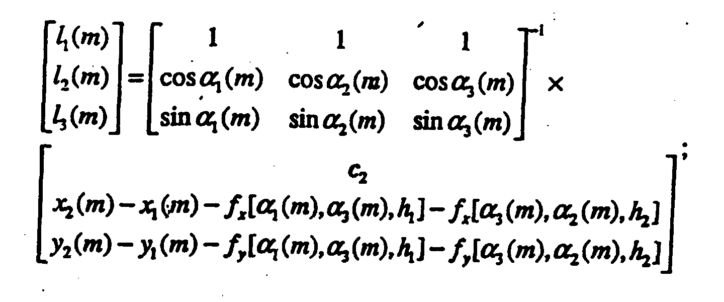
- ⁇ 3 ( m ) ⁇ 1 ( m )+ ⁇ 2 ( m ) 2 + c 1 ; and the lengths of the 3 straight segments, l 1 ( m ), l 2 ( m ), and l 3 ( m ) substantially equal to: where c 1 and c 2 are constants, which do not change for all waveguides in the array.
- f x and f y are functions that give the x- and y-displacements of the curves and transition sections given the starting angle, stopping angle, and the curve handedness (ie., clockwise or counterclockwise) h .
- Fig 5 is a schematic of an optical device including an array of substantially equal length waveguides according to my invention. Specifically, and with reference now to that Figure, an array of waveguides W 1 , W 2 , W 3 ,... W n , are shown connecting an input coupler P i with an output coupler, P o . As should be noted, the waveguides need not originate or terminate at the same coupler(s) as depicted in this Figure for simplicity.
- Each of the waveguides, W 1 , W 2 , W 3 ,... W n are substantially the same total length, and each include a plurality of straight segments, a plurality of curved segments, and optionally, one or more transition segments.
- the total length of the straight segments for an individual waveguide, i.e., W 1 will be substantially the same for any of the other waveguides, i.e., W n .
- the total length of the curved segments for an individual waveguide, i.e., W 1 will be substantially the same for any of the other waveguides, i.e., W n .
- transition segments are present, the total length of the transition segments for an individual waveguide, i.e., W 1 , will be substantially the same for any of the other waveguides, i.e., W n .
- Fig 6. shows the spectral response through a wavelength cross connect as described in the Doerr Optical Cross Connect Article made in silica waveguides wherein Fig 6(a) connecting waveguide paths between waveguide grating routers are designed to have equal lengths but the sum of the straight segment length are NOT equal for each path, while in Fig 6(b), they are.
- all of the path lengths are equal in an actual device, all of the passbands should exhibit the same height. However, if the actual path lengths are more than approximately 0.001% in error, relative to each other, the passband heights will exhibit significant variation.
- the present invention causes the actual waveguide path lengths to be nearly identical in a real device.
- My method gives fabrication tolerant relative path lengths because in the fabrication of planar lightwave circuit waveguides, it is difficult to achieve a precise waveguide width. However, any waveguide width inaccuracy is usually the same for all of the waveguides. A change in waveguide width changes the effective index of the waveguide, changing its effective path length; and this effect is different for straight sections and curved sections. However, since the total straight length and total curved length are independently the same for each waveguide path in the array, the total path lengths will remain equal despite fabrication waveguide width inaccuracies. This method gives also polarization-independent relative path lengths because, again, the total straight length and total curved length are the same for each waveguide path in the array. Because the birefringences of the straight and curved sections are different, other methods may give rise to a polarization dependence in the path-length difference between the waveguide paths.
Landscapes
- Physics & Mathematics (AREA)
- Engineering & Computer Science (AREA)
- Microelectronics & Electronic Packaging (AREA)
- General Physics & Mathematics (AREA)
- Optics & Photonics (AREA)
- Optical Integrated Circuits (AREA)
Abstract
Description
- This invention relates to optical devices and, more particularly, to an optical device having equal-length waveguide paths exhibiting greater fabrication tolerance and reduced polarization sensitivity.
- A Wavelength-Division-Multiplexing (WDM) cross-connect (a non-wavelength-changing one) is a device that can exchange any wavelength channel in any line with the same wavelength channel in any other line. The conventional design is to use a matrix of switches between sets of wavelength multiplexers, such as Waveguide Grating Routers (WGRs). For example see the publications
- [1] M. K. Smit, "New focusing and dispersive planar component based on an optical phased array," Electron. Lett., vol. 24, pp. 385-386 (1988);
- [2] H. Takahasbi, S. Suzuki, K. Kato and I. Nishi, "Arrayed-waveguide grating for wavelength division multi/demultiplexer with nanometer resolution," Electron. Lett., vol. 26, pp. 87-88 (1990); and
- [3] C. Dragone, "An N x N optical multiplexer using a planar arrangement of two star couplers," IEEE Photon. Technol. Lett., vol. 3, 812-814 (1991); each of which are incorporated herein by reference.
-
- For 2 line x 2 line versions, designs have been demonstrated with discrete components {e.g., see B. Glance, "Tunable add drop optical filter providing arbitrary channel arrangements," IEEE Photon. Technol. Lett., vol. 7, 1303-1305 (1995)} which is incorporated herein by reference, and with fully integrated components {e.g., see K. Okamoto, M. Okuno, A. Himeno, and Y. Obmori, "16-channel optical add/drop multiplexer consisting of arrayed-waveguide gratings and double-gate switches," Electron. Lett., vol. 32, 1471-1472 (1996)}, also incorporated herein by reference.
- Referring to the drawing, Fig 1. is a top view of a prior-an
waveguide array multiplexer 10 comprising afirst array coupler 11 coupled via an array of n waveguides W 1, W 2, ..., W n to asecond array coupler 12. Thearray couplers coupler 11 receives light at P i from aninput waveguide 13, andcoupler 12 distributes received light to a pair ofoutput waveguides couplers - In operation, light in the fundamental mode of
input waveguide 13 spreads by diffraction from the center ofcoupler 11, forming a circular wavefront of constant phase. The waveguides around the circumference ofcoupler 11 are all excited with the same phase. Since the waveguides separate, the optical signals become decoupled. After decoupling, however, the light in the waveguides initially continues with a circular phase front and retains nearly the same amplitude distribution as when the waveguides were initially excited. - The array is designed such that each successive waveguide has an increased length Δl compared to its lower neighbor, and the waveguides terminate in a converging circle at
coupler 12. Ifcoupler 12 forms a circular wave converging on the coupler axis at P o. At a different wavelength λo + Δλ, the phase front emerging from the array will be tilted at a small angle , relative to the coupler axis CC' and will couple efficiently near P o towaveguide 15 which is angularly displaced by from the coupler axis. In this example,output waveguide 14 is positioned to couple to λo andoutput waveguide 15 to λo + Δλ. This device can thus be used to receive a two wavelength input from waveguide 13 (λo and λo + Δλ) and provide wavelength separated outputs λo at 14 and λo + Δλ at 15. The device thus acts as a grating and a demultiplexer. In the reverse direction, it can act as a multiplexer. - Many lightwave devices require an array of two or more waveguide paths of substantially equal length, such as dynamic wavelength equalizers disclosed by C. R. Doerr, in an article entitled "Proposed optical cross connect using a planar arrangement of waveguide grating routers and phase shifters," that appeared in IEEE Photon. Technol. Lett., vol. 10, pp. 528-530, 1998 (hereinafter the "Doerr Optical Cross Connect Article"); the wavelength cross connects disclosed by C. R. Doerr and C. Dragone, in another article entitled "Proposed optical cross connect using a planar arrangement of beam steerers," to appear in IEEE Photon. Technol. Lett., vol. 11, February, 1999; and optical cross connects such as that disclosed by C. R. Doerr, C. H. Joyner, and L. W. Stulz, in an article entitled "Integrated WDM dynamic power equalizer with potentially low insertion loss," IEEE Photon. Technol. Lett., vol. 10, pp. 1443-1445, 1998, all incorporated herein by reference.
- Fig. 2 shows a schematic of a prior art device disclosed in United States Patent No. 5,212,758 issued to Adar et al on May 18, 1993 for a "Planar Lens and Low Order Array Multiplexer", equivalent to EP-A-0565308. The device shown in Fig. 2. is similar to that of Fig. 1 except that the n waveguides (W 1, W2 , ..., W n) between
array couplers couplers - Notwithstanding these advances, there is a continuing need for optical devices that facilitate the transmission and management of optical signals.
- I have invented an optical device having an array of substantially equal-length optical waveguides. Each one of the optical waveguides includes one or more straight sections, one or more curved sections, and optionally, one or more transition sections. Unlike the prior art and according to my invention, a total straight section length will be substantially the same for all of the waveguides in the array. Similarly, a total curved section length may be substantially the same for all of the waveguides as well.
- In the drawing,
- Fig. 1 is a schematic view of a prior art waveguide array multiplexer having "C" shaped optical waveguides of unequal length;
- Fig. 2 shows an illustrative prior art "S" shaped optical waveguide useful in optical devices having equal length waveguides;
- Fig. 3 shows an "S" shaped optical waveguide connecting a pair of points;
- Fig. 4 shows an "S" shaped optical waveguide according to the present invention;
- Fig. 5 is a schematic view of a device having an array of "S" shaped optical waveguides according to the present invention; and
- Fig. 6 (a) is a graph showing a spectral response at various wavelengths for an arrayed waveguide constructed according to prior art teachings of the Doerr Optical Cross Connect Article in which total straight segment length is not constant and (b) constructed according to the present teachings wherein total straight segment lengths are constant across all of the individual waveguides.
-
- By way of further background, the fact that the "S" configuration of waveguides can be designed to provide substantially equal path lengths from 21 to 22 can be seen from Fig. 1 by considering a line of symmetry AA' perpendicular to the line P 0 P i in the "C" configuration device. In the Fig. 1 device, the relationship between waveguide and pathlength is given by:
W W - With reference now to Fig. 3, there is shown a generalized waveguide W g having two endpoints P i and P o. In the general case, each waveguide path m must start at a specified point [x 1(m),y 1(m)], where x and y are Cartesian coordinates, at a specified angle α1(m) and must end at another specified point [x 2(m),y 2(m)] at another specified angle α2(m). As can be appreciated, there are an infinite number of waveguide paths possible to effect optical connections between P i and P o, such as the method described in the aforementioned United States Patent No. 5,212,758. Unlike this prior art method, however, my inventive method and apparatus defines the waveguide paths such that the relative length of each path is fabrication tolerant and polarization insensitive.
- My inventive apparatus may be summarized as follows. Each path (waveguide) may include a number of straight segments, i.e., 3; a number of curved segments, i.e., 2, and, optionally, one or more transition segments. Generally speaking, a straight segment has a substantially straight central axis and a curved segment has a central axis that is uniformly curved around a point resulting in a substantially constant radius of curvature. In a particular embodiment in which a number of equal-length waveguides optically connect two endpoints, the straight segments of the waveguides may all have the same width; the curved segments of the waveguides may all have the same bend radius, width, and radial offset; and the transition segments may all be the same for all the waveguide paths. Importantly, the sum of the straight segment lengths is substantially the same for each of the waveguides, and likewise substantially the same for the sum of the curved segment lengths and substantially the same for the sum of the transition segment lengths.
- Fig 4. shows a schematic of an exemplary optical waveguide constructed according my teachings. Specifically, the optical waveguide optically connects two endpoints (x 1,y 1), and (x 2,y 2). As shown in this Figure, the waveguide has a number of straight segments (3 in this example) and a number of curved segments (2 in this example) and, optionally, one or more transition segments interposed between the curved sgments and the straight segments. Not explicitly shown in this Figure, but that which can be readily appreciated by those skilled in the art, such an optical waveguide would have a central axis through which optical signals may propagate. As noted earlier, straight segments exhibit a substantially straight central axis and curved segments exhibit a central axis having a constant radius of curvature.
- These characteristics may be achieved by making the angle of the center straight segment α 3(m) substantially equal to:
c where c 1 and c 2 are constants, which do not change for all waveguides in the array. Additionally, fx and fy are functions that give the x- and y-displacements of the curves and transition sections given the starting angle, stopping angle, and the curve handedness (ie., clockwise or counterclockwise) h.
- Fig 5 is a schematic of an optical device including an array of substantially equal length waveguides according to my invention. Specifically, and with reference now to that Figure, an array of waveguides W 1, W 2, W 3,... W n, are shown connecting an input coupler P i with an output coupler, P o. As should be noted, the waveguides need not originate or terminate at the same coupler(s) as depicted in this Figure for simplicity.
- Each of the waveguides, W 1, W 2, W 3,... W n, are substantially the same total length, and each include a plurality of straight segments, a plurality of curved segments, and optionally, one or more transition segments. As noted before, the total length of the straight segments for an individual waveguide, i.e., W 1, will be substantially the same for any of the other waveguides, i.e., W n. Similarly, the total length of the curved segments for an individual waveguide, i.e., W 1, will be substantially the same for any of the other waveguides, i.e., W n. Finally, if transition segments are present, the total length of the transition segments for an individual waveguide, i.e., W 1, will be substantially the same for any of the other waveguides, i.e., W n.
- Fig 6. shows the spectral response through a wavelength cross connect as described in the Doerr Optical Cross Connect Article made in silica waveguides wherein Fig 6(a) connecting waveguide paths between waveguide grating routers are designed to have equal lengths but the sum of the straight segment length are NOT equal for each path, while in Fig 6(b), they are. When all of the path lengths are equal in an actual device, all of the passbands should exhibit the same height. However, if the actual path lengths are more than approximately 0.001% in error, relative to each other, the passband heights will exhibit significant variation. Advantageously, and as one can see from Fig 6(b), the present invention causes the actual waveguide path lengths to be nearly identical in a real device.
- My method gives fabrication tolerant relative path lengths because in the fabrication of planar lightwave circuit waveguides, it is difficult to achieve a precise waveguide width. However, any waveguide width inaccuracy is usually the same for all of the waveguides. A change in waveguide width changes the effective index of the waveguide, changing its effective path length; and this effect is different for straight sections and curved sections. However, since the total straight length and total curved length are independently the same for each waveguide path in the array, the total path lengths will remain equal despite fabrication waveguide width inaccuracies. This method gives also polarization-independent relative path lengths because, again, the total straight length and total curved length are the same for each waveguide path in the array. Because the birefringences of the straight and curved sections are different, other methods may give rise to a polarization dependence in the path-length difference between the waveguide paths.
Claims (9)
- An optical device comprising an array of substantially equal-length optical wavelengths CHARACTERIZED IN THAT:each one of the optical waveguides has a plurality of straight segments and a plurality of curved segments wherein the sum of the lengths of the straight segments in each of the waveguides is substantially equal.
- An optical device comprising an input, an output, and an array of substantially equal-length optical waveguides optically coupling the input to the output wherein each one of the optical waveguides has a plurality of straight segments and one or more curved segments and the sum of the lengths of the straight segments in each of the waveguides is substantially equal.
- The optical device of claim 2 in which each one of the optical waveguides has a plurality of transition segments wherein the sum of the lengths of the transition segments in each of the waveguides is substantially equal.
- An optical device comprising:an input coupling;an array of substantially equal-length optical waveguides optically coupled to the input coupling, each optical waveguide including:at least three (3) straight segments; andat least two (2) curved segments interposed between the straight segments; wherein the sum of the lengths of the straight segments in each of the waveguides is substantially equal.
- The optical device of claim 4 in which each optical waveguide includes:a plurality of transition segments interposed between the straight segments and the curved segments.
- The optical device of any of the preceding claims in which the sum of the lengths of the curved segments in each of the waveguides is substantially equal.
- The optical device of any of the preceding claims wherein each of the straight segments have substantially the same width.
- The optical device of any of the preceding claims wherein each of the curved segments have substantially the same bend radius, width and radial offset.
- The optical device of claim 4 or claim 5 in which each of the waveguides m starts at a point [x 1(m),y 1(m)], where x and y are Cartesian coordinates, at a starting specified angle α1(m) and ends at another specified point [x 2(m),y 2(m)] at an ending specified angle α2(m), wherein an angle of the center straight segment α3(m) is substantially equal to:where c 1 and c 2 are constants,fx and fy are functions that give the x- and y-displacements of the curves and transition sections given the starting specified angle, ending specified angle, and a curve handedness (i.e., clockwise or counterclockwise) h.
Applications Claiming Priority (2)
| Application Number | Priority Date | Filing Date | Title |
|---|---|---|---|
| US09/232,109 US6219471B1 (en) | 1999-01-15 | 1999-01-15 | Optical device having equal length waveguide paths |
| US232109 | 1999-01-15 |
Publications (2)
| Publication Number | Publication Date |
|---|---|
| EP1020740A1 true EP1020740A1 (en) | 2000-07-19 |
| EP1020740B1 EP1020740B1 (en) | 2006-11-02 |
Family
ID=22871911
Family Applications (1)
| Application Number | Title | Priority Date | Filing Date |
|---|---|---|---|
| EP00300041A Expired - Lifetime EP1020740B1 (en) | 1999-01-15 | 2000-01-06 | Optical device having equal length waveguide paths |
Country Status (3)
| Country | Link |
|---|---|
| US (1) | US6219471B1 (en) |
| EP (1) | EP1020740B1 (en) |
| DE (1) | DE60031587T2 (en) |
Cited By (3)
| Publication number | Priority date | Publication date | Assignee | Title |
|---|---|---|---|---|
| WO2003062888A3 (en) * | 2002-01-21 | 2003-12-18 | Bookham Technology Plc | Array waveguide grating |
| EP1402294A4 (en) * | 2001-05-17 | 2006-11-02 | Optronx Inc | OPTICAL WAVEGUIDE DEVICES WITH MULTIPLE LOADS |
| US20220221714A1 (en) * | 2021-01-12 | 2022-07-14 | Globalfoundries U.S. Inc. | Waveguide bus with balanced optical waveguides and method, system, and software tool for automatic generation of a layout for the waveguide bus |
Families Citing this family (8)
| Publication number | Priority date | Publication date | Assignee | Title |
|---|---|---|---|---|
| US6895133B1 (en) | 2001-06-20 | 2005-05-17 | Lightwave Microsystems Corporation | Crack propagation stops for dicing of planar lightwave circuit devices |
| IL145320A (en) * | 2001-09-06 | 2006-12-10 | Gilad Optical Switches Ltd | Tunable optical filter |
| KR100401203B1 (en) * | 2001-11-13 | 2003-10-10 | 삼성전자주식회사 | Planar lightwave circuit with polynomial curve waveguide |
| US7003198B2 (en) * | 2003-09-09 | 2006-02-21 | Lucent Technologies Inc. | Integrateable band filter using waveguide grating routers |
| US8363987B2 (en) | 2009-09-02 | 2013-01-29 | International Business Machines Corporation | Multi-mode multiplexing using staged coupling and quasi-phase-matching |
| US11448823B1 (en) * | 2017-08-18 | 2022-09-20 | Acacia Communications, Inc. | Method, system, and apparatus for a LiDAR sensor with a large grating |
| CN112204457B (en) * | 2018-04-24 | 2024-01-19 | 株式会社大成科技 | Optical phased array and LiDAR sensor using the same |
| WO2019220513A1 (en) * | 2018-05-14 | 2019-11-21 | 株式会社大成テクノロジー | OPTICAL INTEGRATED CIRCUIT, AND OPTICAL PHASED ARRAY AND LiDAR SENSOR WHICH USE SAME |
Citations (3)
| Publication number | Priority date | Publication date | Assignee | Title |
|---|---|---|---|---|
| EP0565308A1 (en) * | 1992-04-10 | 1993-10-13 | AT&T Corp. | Planar lens and low order array multiplexer |
| EP0823647A2 (en) * | 1996-08-06 | 1998-02-11 | Nippon Telegraph And Telephone Corporation | Arrayed-waveguide grating |
| US5822481A (en) * | 1995-12-28 | 1998-10-13 | Alcatel Optronics | Waveguide grating optical demultiplexer |
Family Cites Families (2)
| Publication number | Priority date | Publication date | Assignee | Title |
|---|---|---|---|---|
| DE4427523C1 (en) * | 1994-08-03 | 1996-01-11 | Iot Integrierte Optik Gmbh | Asymmetric integrated optical Mach-Zehnder interferometer |
| EP0792469A1 (en) * | 1995-09-20 | 1997-09-03 | Koninklijke Philips Electronics N.V. | Integrated optical circuit comprising a polarization convertor |
-
1999
- 1999-01-15 US US09/232,109 patent/US6219471B1/en not_active Expired - Lifetime
-
2000
- 2000-01-06 EP EP00300041A patent/EP1020740B1/en not_active Expired - Lifetime
- 2000-01-06 DE DE60031587T patent/DE60031587T2/en not_active Expired - Lifetime
Patent Citations (3)
| Publication number | Priority date | Publication date | Assignee | Title |
|---|---|---|---|---|
| EP0565308A1 (en) * | 1992-04-10 | 1993-10-13 | AT&T Corp. | Planar lens and low order array multiplexer |
| US5822481A (en) * | 1995-12-28 | 1998-10-13 | Alcatel Optronics | Waveguide grating optical demultiplexer |
| EP0823647A2 (en) * | 1996-08-06 | 1998-02-11 | Nippon Telegraph And Telephone Corporation | Arrayed-waveguide grating |
Non-Patent Citations (1)
| Title |
|---|
| DOERR C R ET AL: "PROPOSED OPTICAL CROSS CONNECT USING A PLANAR ARRANGEMENT OF BEAM STEERERS", IEEE PHOTONICS TECHNOLOGY LETTERS,US,IEEE INC. NEW YORK, vol. 11, no. 2, February 1999 (1999-02-01), pages 197 - 199, XP000803427, ISSN: 1041-1135 * |
Cited By (4)
| Publication number | Priority date | Publication date | Assignee | Title |
|---|---|---|---|---|
| EP1402294A4 (en) * | 2001-05-17 | 2006-11-02 | Optronx Inc | OPTICAL WAVEGUIDE DEVICES WITH MULTIPLE LOADS |
| WO2003062888A3 (en) * | 2002-01-21 | 2003-12-18 | Bookham Technology Plc | Array waveguide grating |
| US20220221714A1 (en) * | 2021-01-12 | 2022-07-14 | Globalfoundries U.S. Inc. | Waveguide bus with balanced optical waveguides and method, system, and software tool for automatic generation of a layout for the waveguide bus |
| US11500198B2 (en) * | 2021-01-12 | 2022-11-15 | Globalfoundries U.S. Inc. | Waveguide bus with balanced optical waveguides and method, system, and software tool for automatic generation of a layout for the waveguide bus |
Also Published As
| Publication number | Publication date |
|---|---|
| EP1020740B1 (en) | 2006-11-02 |
| DE60031587T2 (en) | 2007-06-21 |
| DE60031587D1 (en) | 2006-12-14 |
| US6219471B1 (en) | 2001-04-17 |
Similar Documents
| Publication | Publication Date | Title |
|---|---|---|
| EP1170605B1 (en) | Planar waveguide grating device having a passband with a flat-top and sharp-transitions | |
| JP3338356B2 (en) | Optical device | |
| US6049640A (en) | Wavelength-division-multiplexing cross-connect using angular dispersive elements and phase shifters | |
| US6351581B1 (en) | Optical add-drop multiplexer having an interferometer structure | |
| EP1191364B1 (en) | Waveguide optical interferometer | |
| US5212758A (en) | Planar lens and low order array multiplexer | |
| US6266464B1 (en) | Optical arrayed waveguide grating devices | |
| US6141467A (en) | Wavelength-division-multiplexing programmable add/drop using interleave-chirped waveguide grating router | |
| EP1020740B1 (en) | Optical device having equal length waveguide paths | |
| JPH05323246A (en) | Optical multiplexer / demultiplexer | |
| JPH05313029A (en) | Light wave combining/splitting instrument | |
| US20230161101A1 (en) | Devices and methods exploiting waveguide supercells | |
| US6787868B1 (en) | Microlenses for integrated optical devices | |
| Doerr et al. | Compact and low-loss manner of waveguide grating router passband flattening and demonstration in a 64-channel blocker/multiplexer | |
| US6735363B1 (en) | Waveguide-grating router with output tapers configured to provide a passband that is optimized for each channel individually | |
| US7433560B2 (en) | Rectangular-passband multiplexer | |
| US6807354B2 (en) | Waveguide optical device | |
| JP3042664B2 (en) | Optical frequency selection switch | |
| JP2004101995A (en) | Optical coupling / branching element | |
| JPH0798419A (en) | Integrated optical waveguide circuit | |
| JP2001514766A (en) | Wavelength-selective optical device including at least one Bragg grating structure | |
| US7058262B2 (en) | Arrayed waveguide grating | |
| JP3396477B2 (en) | Integrated optical waveguide circuit | |
| WO2001033269A1 (en) | Grating waveguide configuration for phasars | |
| Tervonen | Glass waveguide WDM devices: design and analysis |
Legal Events
| Date | Code | Title | Description |
|---|---|---|---|
| PUAI | Public reference made under article 153(3) epc to a published international application that has entered the european phase |
Free format text: ORIGINAL CODE: 0009012 |
|
| AK | Designated contracting states |
Kind code of ref document: A1 Designated state(s): DE FR GB IT |
|
| AX | Request for extension of the european patent |
Free format text: AL;LT;LV;MK;RO;SI |
|
| 17P | Request for examination filed |
Effective date: 20001214 |
|
| AKX | Designation fees paid |
Free format text: DE FR GB IT |
|
| 17Q | First examination report despatched |
Effective date: 20050616 |
|
| GRAP | Despatch of communication of intention to grant a patent |
Free format text: ORIGINAL CODE: EPIDOSNIGR1 |
|
| GRAS | Grant fee paid |
Free format text: ORIGINAL CODE: EPIDOSNIGR3 |
|
| GRAA | (expected) grant |
Free format text: ORIGINAL CODE: 0009210 |
|
| AK | Designated contracting states |
Kind code of ref document: B1 Designated state(s): DE FR GB IT |
|
| REG | Reference to a national code |
Ref country code: GB Ref legal event code: FG4D |
|
| REF | Corresponds to: |
Ref document number: 60031587 Country of ref document: DE Date of ref document: 20061214 Kind code of ref document: P |
|
| ET | Fr: translation filed | ||
| PLBE | No opposition filed within time limit |
Free format text: ORIGINAL CODE: 0009261 |
|
| STAA | Information on the status of an ep patent application or granted ep patent |
Free format text: STATUS: NO OPPOSITION FILED WITHIN TIME LIMIT |
|
| 26N | No opposition filed |
Effective date: 20070803 |
|
| REG | Reference to a national code |
Ref country code: GB Ref legal event code: 732E Free format text: REGISTERED BETWEEN 20131121 AND 20131127 |
|
| REG | Reference to a national code |
Ref country code: FR Ref legal event code: CD Owner name: ALCATEL-LUCENT USA INC. Effective date: 20131122 |
|
| REG | Reference to a national code |
Ref country code: FR Ref legal event code: GC Effective date: 20140410 |
|
| REG | Reference to a national code |
Ref country code: FR Ref legal event code: RG Effective date: 20141015 |
|
| REG | Reference to a national code |
Ref country code: FR Ref legal event code: PLFP Year of fee payment: 16 |
|
| REG | Reference to a national code |
Ref country code: FR Ref legal event code: PLFP Year of fee payment: 17 |
|
| REG | Reference to a national code |
Ref country code: FR Ref legal event code: PLFP Year of fee payment: 18 |
|
| PGFP | Annual fee paid to national office [announced via postgrant information from national office to epo] |
Ref country code: DE Payment date: 20170120 Year of fee payment: 18 Ref country code: FR Payment date: 20170120 Year of fee payment: 18 |
|
| PGFP | Annual fee paid to national office [announced via postgrant information from national office to epo] |
Ref country code: GB Payment date: 20170119 Year of fee payment: 18 |
|
| PGFP | Annual fee paid to national office [announced via postgrant information from national office to epo] |
Ref country code: IT Payment date: 20170124 Year of fee payment: 18 |
|
| REG | Reference to a national code |
Ref country code: DE Ref legal event code: R119 Ref document number: 60031587 Country of ref document: DE |
|
| GBPC | Gb: european patent ceased through non-payment of renewal fee |
Effective date: 20180106 |
|
| PG25 | Lapsed in a contracting state [announced via postgrant information from national office to epo] |
Ref country code: DE Free format text: LAPSE BECAUSE OF NON-PAYMENT OF DUE FEES Effective date: 20180801 Ref country code: FR Free format text: LAPSE BECAUSE OF NON-PAYMENT OF DUE FEES Effective date: 20180131 |
|
| REG | Reference to a national code |
Ref country code: FR Ref legal event code: ST Effective date: 20180928 |
|
| PG25 | Lapsed in a contracting state [announced via postgrant information from national office to epo] |
Ref country code: GB Free format text: LAPSE BECAUSE OF NON-PAYMENT OF DUE FEES Effective date: 20180106 |
|
| PG25 | Lapsed in a contracting state [announced via postgrant information from national office to epo] |
Ref country code: IT Free format text: LAPSE BECAUSE OF NON-PAYMENT OF DUE FEES Effective date: 20180106 |
|
| REG | Reference to a national code |
Ref country code: DE Ref legal event code: R081 Ref document number: 60031587 Country of ref document: DE Owner name: WSOU INVESTMENTS, LLC, LOS ANGELES, US Free format text: FORMER OWNER: LUCENT TECHNOLOGIES INC., MURRAY HILL, N.J., US |