EP1018169B1 - Robust group iii nitride light emitting diode for high reliability in standard packaging applications - Google Patents
Robust group iii nitride light emitting diode for high reliability in standard packaging applications Download PDFInfo
- Publication number
- EP1018169B1 EP1018169B1 EP98945787A EP98945787A EP1018169B1 EP 1018169 B1 EP1018169 B1 EP 1018169B1 EP 98945787 A EP98945787 A EP 98945787A EP 98945787 A EP98945787 A EP 98945787A EP 1018169 B1 EP1018169 B1 EP 1018169B1
- Authority
- EP
- European Patent Office
- Prior art keywords
- light emitting
- emitting diode
- gallium nitride
- layer
- diode
- Prior art date
- Legal status (The legal status is an assumption and is not a legal conclusion. Google has not performed a legal analysis and makes no representation as to the accuracy of the status listed.)
- Expired - Lifetime
Links
Images

Classifications
-
- H—ELECTRICITY
- H01—ELECTRIC ELEMENTS
- H01L—SEMICONDUCTOR DEVICES NOT COVERED BY CLASS H10
- H01L33/00—Semiconductor devices with at least one potential-jump barrier or surface barrier specially adapted for light emission; Processes or apparatus specially adapted for the manufacture or treatment thereof or of parts thereof; Details thereof
- H01L33/44—Semiconductor devices with at least one potential-jump barrier or surface barrier specially adapted for light emission; Processes or apparatus specially adapted for the manufacture or treatment thereof or of parts thereof; Details thereof characterised by the coatings, e.g. passivation layer or anti-reflective coating
-
- H—ELECTRICITY
- H01—ELECTRIC ELEMENTS
- H01L—SEMICONDUCTOR DEVICES NOT COVERED BY CLASS H10
- H01L33/00—Semiconductor devices with at least one potential-jump barrier or surface barrier specially adapted for light emission; Processes or apparatus specially adapted for the manufacture or treatment thereof or of parts thereof; Details thereof
- H01L33/36—Semiconductor devices with at least one potential-jump barrier or surface barrier specially adapted for light emission; Processes or apparatus specially adapted for the manufacture or treatment thereof or of parts thereof; Details thereof characterised by the electrodes
- H01L33/40—Materials therefor
- H01L33/42—Transparent materials
-
- H—ELECTRICITY
- H01—ELECTRIC ELEMENTS
- H01L—SEMICONDUCTOR DEVICES NOT COVERED BY CLASS H10
- H01L2224/00—Indexing scheme for arrangements for connecting or disconnecting semiconductor or solid-state bodies and methods related thereto as covered by H01L24/00
- H01L2224/01—Means for bonding being attached to, or being formed on, the surface to be connected, e.g. chip-to-package, die-attach, "first-level" interconnects; Manufacturing methods related thereto
- H01L2224/42—Wire connectors; Manufacturing methods related thereto
- H01L2224/47—Structure, shape, material or disposition of the wire connectors after the connecting process
- H01L2224/48—Structure, shape, material or disposition of the wire connectors after the connecting process of an individual wire connector
- H01L2224/4805—Shape
- H01L2224/4809—Loop shape
- H01L2224/48091—Arched
-
- H—ELECTRICITY
- H01—ELECTRIC ELEMENTS
- H01L—SEMICONDUCTOR DEVICES NOT COVERED BY CLASS H10
- H01L2224/00—Indexing scheme for arrangements for connecting or disconnecting semiconductor or solid-state bodies and methods related thereto as covered by H01L24/00
- H01L2224/01—Means for bonding being attached to, or being formed on, the surface to be connected, e.g. chip-to-package, die-attach, "first-level" interconnects; Manufacturing methods related thereto
- H01L2224/42—Wire connectors; Manufacturing methods related thereto
- H01L2224/47—Structure, shape, material or disposition of the wire connectors after the connecting process
- H01L2224/48—Structure, shape, material or disposition of the wire connectors after the connecting process of an individual wire connector
- H01L2224/481—Disposition
- H01L2224/48151—Connecting between a semiconductor or solid-state body and an item not being a semiconductor or solid-state body, e.g. chip-to-substrate, chip-to-passive
- H01L2224/48221—Connecting between a semiconductor or solid-state body and an item not being a semiconductor or solid-state body, e.g. chip-to-substrate, chip-to-passive the body and the item being stacked
- H01L2224/48245—Connecting between a semiconductor or solid-state body and an item not being a semiconductor or solid-state body, e.g. chip-to-substrate, chip-to-passive the body and the item being stacked the item being metallic
- H01L2224/48247—Connecting between a semiconductor or solid-state body and an item not being a semiconductor or solid-state body, e.g. chip-to-substrate, chip-to-passive the body and the item being stacked the item being metallic connecting the wire to a bond pad of the item
-
- H—ELECTRICITY
- H01—ELECTRIC ELEMENTS
- H01L—SEMICONDUCTOR DEVICES NOT COVERED BY CLASS H10
- H01L2924/00—Indexing scheme for arrangements or methods for connecting or disconnecting semiconductor or solid-state bodies as covered by H01L24/00
- H01L2924/15—Details of package parts other than the semiconductor or other solid state devices to be connected
- H01L2924/181—Encapsulation
Definitions
- the present invention relates to light emitting diodes and in particular relates to such diodes formed from Group III nitrides in standard packaging applications.
- a light emitting diode is a p-n junction device that converts electrical energy into optical radiation.
- LED's emit external spontaneous radiation in the ultraviolet, visible, and infrared regions of the electromagnetic spectrum.
- shorter wavelengths of light such as blue and ultraviolet
- longer wavelengths such as red and infrared
- the particular portion of the spectrum in which they emit ⁇ i . e ., their color ⁇ is based upon the energy of the transitions that create the emissions.
- the energy of the transitions is determined to a great extent by the bandgap of the particular material.
- the bandgap of the semiconductor material in order for a light emitting diode to emit in the blue or ultraviolet portions of the spectrum, the bandgap of the semiconductor material must be large enough (wide enough) to support a transition with sufficient energy to produce blue or ultraviolet light
- the candidate materials for light emitting diodes in the blue and ultraviolet regions of the spectrum are limited to certain wide bandgap materials such as diamond, silicon carbide (SiC) and Group III nitrides; e.g., binary, ternary and tertiary nitrides formed from the Group III elements of the periodic table such as gallium nitride (GaN), indium gallium nitride (InGaN), and aluminum gallium nitride (AlGaN).
- GaN gallium nitride
- InGaN indium gallium nitride
- AlGaN aluminum gallium nitride
- a light emitting diode generally includes two layers of opposite conductivity type material which together form a p-n junction. These materials are typically in the form of epitaxial layers on a substrate. Most desirably an ohmic contact is made to the substrate and to the top epitaxial layer to form a "vertical" device for optimum efficiency in packaging.
- an LED is often packaged for end use in the form of an LED lamp.
- a typical LED lamp includes an LED chip (or “die”, the term “chip” often being used to describe an integrated circuit rather than an LED) and a plastic (or sometimes glass) lens.
- the lens is colored to serve as an optical filter and to enhance contrast, but for blue LEDs the lens is preferably colorless so as to avoid interference with the desired blue emission.
- Typical lamp configurations are well known to those of ordinary skill in this art and are set forth for example, in Sze, supra at pages 697-700.
- an LED chip is packaged as a lamp, it can be used for a variety of applications such as indicators and alphanumeric displays.
- Group III nitride devices are typically formed on either sapphire or silicon carbide substrates. Silicon carbide substrates are preferred in many circumstances because SiC can be conductively doped. Thus, an SiC substrate can form the basis for a "vertical" device with "top” and “bottom” ohmic contacts. In contrast, the insulating character of sapphire prevents its use in vertical devices.
- n-type SiC substrates tend to be preferred over p-type substrates because n-type SiC is generally more conductive and transmits more light.
- a Group III nitride device on an SiC substrate typically includes an n-type substrate, an n-type buffer layer (or combination of layers), an n-type epitaxial layer, and the p-type layer (e.g., GaN) on the "top" of the device.
- the packaging itself is very specific and robust because the LED chip being packaged is relatively fragile even under normal environmental circumstances.
- the p-type layer, the ohmic contact, and the passivation layer are coated with a flexible transparent polymeric material and then encapsulated in a hard resin such as an epoxy-based polymer.
- Nakamura et al. report that, "(t)he p-electrode (to the p-type gallium nitride) may be formed of any suitable metallic material" (page 6, line 7).
- Nakamura goes on to list eight candidate metals (Au, Ni, Pt, Al, Sn, In, Cr, and Ti) and names a nickel and gold combination (page 6, lines 10-12 and 33-35) as the preferred selection.
- Nakamura offers some merely general criteria ("The material forming the protective film is not particularly limited, as long as it is transparent, and electrically insulative.” Page 9, lines 31-32). Nakamura then goes on to list four candidate materials: silicon dioxide (SiO 2 ), titanium oxide (TiO), aluminum oxide (Al 2 O 3 ), and Silicon nitride (Si 3 N 4 ).
- LEDs that: (1) include a top epitaxial layer of p-type GaN; (2) use ohmic contacts formed from certain metals (or their combinations) such as titanium and gold ("Ti/Au"); and (3) use silicon dioxide (SiO 2 ) as the passivation layer, tend to exhibit more rapid degradation than is commercially acceptable. More specifically, it appears that the water-permeability of SiO 2 allows sufficient moisture to reach the p-electrode to degrade the electrode and eventually the entire device relatively quickly.
- blue LEDs formed from Group III nitrides must be manufactured in such a manner that they can be incorporated in more common lamp packages analogous to the lamp packages used for materials that are less esoteric than Group III nitrides.
- the invention meets this object with a diode that comprises a Group III heterojunction diode with a p-type Group III nitride (and preferably gallium nitride) contact layer, an ohmic contact to the p-type contact layer, and a passivation layer on the ohmic contact, characterized in that the diode will emit at least 50% of its original optical power and remain substantially unchanged in operating voltage after operating for at least 1000 hours at 10 milliamps in an environment of 85% relative humidity at a temperature of 85°C.
- the invention comprises an LED lamp formed of the light emitting diode and a plastic lens.
- the present invention is a physically robust light emitting diode that offers high reliability in standard packaging and will withstand high temperature and high humidity conditions.
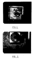
- Figure 1 is a photograph of an entire LED ("die").
- the passivation layer of silicon dioxide (glass) has been removed except around the outside edge of the die.
- the portions where glass is still present are generally indicated by the spotted or stained-appearing portions around the perimeter of the generally square die.
- This mottled appearance results from a varying gap of air under the glass as it delaminates from the die.
- the delamination begins at about the three o'clock (moving clockwise) and reaches approximately the 11:00 o'clock position.
- the passivation layer is absent from the center of the die and the wire ball bond can be seen at the very center of the die still attached to the bond pad.
- the center portion of the passivation layer was removed while the die was being de-encapsulated after testing.
- the passivation layer of the die illustrated in Figure I had delaminated in the package during testing, and allowed moisture to penetrate beneath the passivation layer.
- the resulting delamination reduced the initial light output of this particular device by about 20%.
- the moisture which tends to permeate through the epoxy lens of an LED lamp and around the leads coming out of the bottom of the lamp package, causes the thin semi-transparent ohmic contact to degrade and eventually fail completely. This failure in turn causes the light output to continue to fall and eventually increase the forward voltage of the device.
- the failure of the contact appears as the dark or rough areas just to the right of the center of the die.
- Figure 2 is a magnified view of the die photographed in Figure 1.
- Figure 2 illustrates that the glass remaining on the perimeter has broken off of the inner mesa of the device and that the p-contact has failed.
- the dark, rough appearing areas are positions where the ohmic contact (titanium and gold in this example) has balled up.
- the contact becomes less compatible with the p-type layer it tends to bead up rather than wet the p-type layer.
- the Ti/Au balls up around the bond pad the device slowly becomes disconnected.
- light is no longer generated in areas where the contact becomes discontinuous. Because a p-type gallium nitride surface is not a good conductor, and generally exhibits high resistivity, the poor current spreading in the void areas fail to provide a current path which would help generate light.
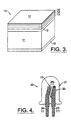
- FIG. 3 illustrates a first embodiment of the diode of the invention that will withstand high temperature and high humidity conditions.
- the diode is generally designated at 10 and includes a silicon carbide substrate 11, the production and nature of which are clearly set forth in other U.S. patents assigned to assignee of this invention, including for example No. RE 34,861 (formerly No. 4,866,005).
- the silicon carbide substrate is a single crystal selected from the group consisting of the 3C, 4H, 6H, and 15R polytypes of silicon carbide.
- the LED of the present invention further comprises a buffer structure 12 on the silicon carbide substrate 11.
- the buffer structure helps provide a crystalline and mechanical transition from the silicon carbide substrate 11 to the remaining Group III nitride portions of the device.
- Appropriate buffer structures are set forth for example in U.S. Patents Nos. 5,393,993; 5,523,589; 5,592,501, and 5,739,554, all of which are commonly assigned with the present invention.
- the diode 10 further comprises a Group III nitride heteroj unction diode structure 13 with a p-type Group III nitride contact layer 14 on the buffer structure 12.
- An ohmic contact 15 is made to the substrate 11 and another ohmic contact 16 is made to the p-type gallium nitride epitaxial layer.
- the ohmic contact 16 is selected from the group consisting of platinum, palladium, gold, a combination of titanium and gold, a combination of platinum and gold, a combination of titanium, platinum and gold, or a combination of platinum and indium tin oxide, and is most preferably formed of platinum or palladium.
- the device is completed with a passivation layer 17 on the ohmic contact 16, of which appropriate candidate materials are recited above, but that is most preferably formed of silicon nitride.
- the p-type contact layer is gallium nitride and the ohmic contact is platinum.
- the heterostructure diode is a double heterostructure that includes an n-type gallium nitride epitaxial layer on the buffer structure, an n-type aluminum gallium nitride epitaxial layer on the n-type gallium nitride layer, a compensated n-type gallium nitride active layer on the n-type aluminum gallium nitride layer, and a p-type aluminum gallium nitride layer on the gallium nitride active layer, with a p-type gallium nitride contact layer on the p-type aluminum gallium nitride layer.
- Table 1 summarizes these ohmic contact materials in terms of their suitability for devices according to the claimed invention.
- A refers to superior characteristics
- C refers to generally weak characteristics.
- the ohmic contact 16 covers a substantial portion of the p-type gallium nitride layer to encourage current spreading across the p-type gallium nitride layer. Because it covers the light emitting portions of the device, the ohmic contact 16 is preferably thin enough to be semi-transparent.
- the invention comprises a physically robust light emitting diode that includes the p-type contact layer 14, the ohmic contact 16 to the p-type layer 14 and the passivation layer 17, but characterized in that the diode will emit at least 50% of its original optical power and remain substantially unchanged in operating voltage after operating for at least 1000 hours at 10 milliamps in an environment of 85% relative humidity at a temperature of 85°C. These conditions are known as the "85/85/10" test for purposes of determining diode reliability under extreme, yet expected operating conditions.
- the original optical power is generally high, for example about 800 microwatts at 20 milliamps of forward current input or even about 1600 microwatt at 20 milliamps of current input.
- the ability of devices with such output to maintain at least 50% of their original optical power after the 85/85/10 test will be recognized as a significant advance in such diodes.
- the diodes illustrated in Figure 3 can be used in a number of specific applications.
- One useful application is as a display, typically referred to as “numeric” or “alphanumeric” displays, although certainly not limited to such, that incorporate a plurality of the light emitting diodes according to the invention.
- blue emitting diodes according to the present invention are incorporated with red and green LEDs to form red-green-blue (“RGB”) pixels. Because such pixels individually produce the three primary colors, they have the capability to produce almost all colors visible to the human eye.
- RGB red-green-blue
- diodes such as the diode 10 illustrated in Figure 3 are incorporated into LED lamps.
- Figure 4 accordingly illustrates one version of such a typical lamp. It will understood, of course, that Figure 4 is simply exemplary of the type of lamp structure that can be used to incorporate a diode according to the present and is in no sense limiting of the type of lamp with which the diode of the invention can be used.
- the lamp 20 includes the diode 10 according to the invention encapsulated in a plastic (i.e. , polymeric) lens 21.
- the plastic material for the lens can be selected from a wide variety of polymeric materials that are well known to those of ordinary skill in this art and without undue experimentation.
- the lens 21 is formed of an epoxy resin.
- the lamp 20 further comprises a metal lead frame 22 for electrically connecting the lamp to other electronic circuit elements. As illustrated in Figure 4, the metal lead frame 22 incorporates the anode 23 and the cathode 24.
- a plurality of the lamps 20 can be incorporated to form an appropriate display device.
- gallium nitride devices of this type emit in the blue portion of the visible spectrum
- lamps such as those according to the present invention can be advantageously incorporated along with red and green LED lamps to form a full color display. Examples of such displays are set forth in for example WO-A- 97/24706 and US-A- 5,812,105.
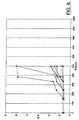
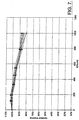
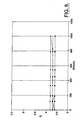
- Figures 5-8 plot some comparative data that highlights the advantages of the present invention.
- Figure 5 plots relative intensity (i.e. , the starting intensity of each diode is considered to be 100%) versus time for certain Group III nitride diodes under the aforementioned 85/85/10 test conditions.
- Figures 5 and 6 reflect data from diodes with p-type gallium nitride (GaN) contact layers, titanium/gold ("Ti/Au”) ohmic contacts, and silicon dioxide (SiO 2 ) passivation layers.
- GaN gallium nitride
- Ti/Au titanium/gold
- SiO 2 silicon dioxide
- Figure 5 illustrates, the diodes begin to degrade immediately, with some dropping below 50% of their original intensity in less than 200 hours.
- Figure 6 plots forward voltage (V f ) versus hours for the same diodes under the same conditions as in Figure 5 and demonstrates that a substantial number of the diodes have significantly degraded within 500 hours.
- Figures 7 and 8 highlight some of the advantages of diodes according to the present invention, and includes diodes with p-type GaN contact layers, platinum (Pt) ohmic contacts, and silicon nitride (Si 3 N 4 ) passivation layers.
- Pt platinum
- Si 3 N 4 silicon nitride
Abstract
Description

Claims (14)
- A high-reliability light emitting diode that will withstand high temperature and high humidity conditions, said diode comprising:characterized bya silicon carbide substrate (11);a buffer structure (12) on said substrate;a Group III nitride heterojunction diode (13) with a p-type Group III nitride contact layer (14) on said buffer structure;an ohmic contact (15) to said substrate;
a platinum ohmic contact (16) to said p-type contact layer; and
a silicon nitride passivation layer (17) on said platinum ohmic contact. - A high reliability light emitting diode according to Claim 1 wherein said diode comprises a single heterojunction diode.
- A high reliability light emitting diode according to Claim 1 wherein said diode comprises a double heterojunction diode.
- A high reliability light emitting diode according to Claim 1 wherein said contact layer comprises gallium nitride
- A high reliability light emitting diode according to Claim 1 wherein said ohmic contact is thin enough to be semi-transparent.
- A pixel comprising:a light emitting diode according to Claim 1 that emits in the blue portion of the visible spectrum;a red light emitting diode; anda green light emitting diode.
- A high reliability light emitting diode according to Claim 1 that is capable of emitting at least 50% of its original optical power and remaining substantially unchanged in operating voltage after operating for at least 1000 hours at 10 milliamps in an environment of 85% relative humidity at a temperature of 85 C.
- A high reliability light emitting diode according to Claim 7 wherein the original optical power is about 800 microwatts at 20 milliamps of forward current input.
- A high reliability light emitting diode according to Claim 7 wherein the original optical power is about 1600 microwatts at 20 milliamps of forward current input.
- A high reliability light emitting diode according to Claim 1 wherein said silicon carbide substrate is a single crystal selected from the group consisting of the 3C, 4H, 6H, and 15R polytypes of silicon carbide
- An LED lamp that incorporates the diode of Claim 1 within a plastic lens.
- A display comprising a plurality of light emitting diodes according to Claim 1, or a plurality of pixels according to Claim 6 or a plurality of LED lamps according to Claim 11.
- A display according to Claim 12 wherein said light emitting diodes or said LED lamps emit in the blue portion of the visible spectrum, and further comprising a plurality of red light emitting diodes or LED lamps and a plurality of green light emitting diodes or LED lamps.
- A high-reliability light emitting diode according to Claim 1 wherein said heterojunction diode and contact layer comprises:an n-type gallium nitride epitaxial layer on said buffer structure;an n-type aluminum gallium nitride epitaxial layer on said gallium nitride layera compensated n-type gallium nitride active layer on said n-type aluminum gallium nitride active layer;a p-type aluminum gallium nitride layer on said gallium nitride active layer; anda p-type gallium nitride contact layer on said p-type aluminum gallium nitride layer.
Applications Claiming Priority (3)
| Application Number | Priority Date | Filing Date | Title |
|---|---|---|---|
| US920409 | 1992-07-27 | ||
| US92040997A | 1997-08-29 | 1997-08-29 | |
| PCT/US1998/017849 WO1999010936A2 (en) | 1997-08-29 | 1998-08-28 | Robust group iii nitride light emitting diode for high reliability in standard applications |
Publications (2)
| Publication Number | Publication Date |
|---|---|
| EP1018169A2 EP1018169A2 (en) | 2000-07-12 |
| EP1018169B1 true EP1018169B1 (en) | 2004-10-13 |
Family
ID=25443701
Family Applications (1)
| Application Number | Title | Priority Date | Filing Date |
|---|---|---|---|
| EP98945787A Expired - Lifetime EP1018169B1 (en) | 1997-08-29 | 1998-08-28 | Robust group iii nitride light emitting diode for high reliability in standard packaging applications |
Country Status (11)
| Country | Link |
|---|---|
| US (1) | US6946682B2 (en) |
| EP (1) | EP1018169B1 (en) |
| JP (2) | JP4597363B2 (en) |
| KR (1) | KR100651145B1 (en) |
| CN (1) | CN1129192C (en) |
| AT (1) | ATE279789T1 (en) |
| AU (1) | AU9295098A (en) |
| CA (1) | CA2299379C (en) |
| DE (1) | DE69827025T2 (en) |
| ES (1) | ES2226169T3 (en) |
| WO (1) | WO1999010936A2 (en) |
Families Citing this family (28)
| Publication number | Priority date | Publication date | Assignee | Title |
|---|---|---|---|---|
| EP1014455B1 (en) | 1997-07-25 | 2006-07-12 | Nichia Corporation | Nitride semiconductor device |
| US6825501B2 (en) * | 1997-08-29 | 2004-11-30 | Cree, Inc. | Robust Group III light emitting diode for high reliability in standard packaging applications |
| EP1018169B1 (en) * | 1997-08-29 | 2004-10-13 | Cree, Inc. | Robust group iii nitride light emitting diode for high reliability in standard packaging applications |
| JP3770014B2 (en) | 1999-02-09 | 2006-04-26 | 日亜化学工業株式会社 | Nitride semiconductor device |
| KR100683877B1 (en) | 1999-03-04 | 2007-02-15 | 니치아 카가쿠 고교 가부시키가이샤 | Nitride Semiconductor Laser Element |
| US6926435B2 (en) * | 2001-08-23 | 2005-08-09 | Wavien, Inc. | Led illumination engine using a reflector |
| US6683327B2 (en) | 2001-11-13 | 2004-01-27 | Lumileds Lighting U.S., Llc | Nucleation layer for improved light extraction from light emitting devices |
| US6900067B2 (en) | 2002-12-11 | 2005-05-31 | Lumileds Lighting U.S., Llc | Growth of III-nitride films on mismatched substrates without conventional low temperature nucleation layers |
| KR101045160B1 (en) * | 2002-12-20 | 2011-06-30 | 크리 인코포레이티드 | Methods of forming semiconductor devices having self aligned semiconductor mesas and contact layers and related devices |
| WO2005124879A1 (en) * | 2004-06-18 | 2005-12-29 | Showa Denko K.K. | Group iii nitride semiconductor light emitting device |
| US7432536B2 (en) * | 2004-11-04 | 2008-10-07 | Cree, Inc. | LED with self aligned bond pad |
| JP2009530798A (en) | 2006-01-05 | 2009-08-27 | イルミテックス, インコーポレイテッド | Independent optical device for directing light from an LED |
| US8101961B2 (en) | 2006-01-25 | 2012-01-24 | Cree, Inc. | Transparent ohmic contacts on light emitting diodes with growth substrates |
| US7646024B2 (en) * | 2006-08-18 | 2010-01-12 | Cree, Inc. | Structure and method for reducing forward voltage across a silicon carbide-group III nitride interface |
| WO2008042351A2 (en) | 2006-10-02 | 2008-04-10 | Illumitex, Inc. | Led system and method |
| US9484499B2 (en) | 2007-04-20 | 2016-11-01 | Cree, Inc. | Transparent ohmic contacts on light emitting diodes with carrier substrates |
| WO2009100358A1 (en) | 2008-02-08 | 2009-08-13 | Illumitex, Inc. | System and method for emitter layer shaping |
| TWI362769B (en) | 2008-05-09 | 2012-04-21 | Univ Nat Chiao Tung | Light emitting device and fabrication method therefor |
| TW201034256A (en) | 2008-12-11 | 2010-09-16 | Illumitex Inc | Systems and methods for packaging light-emitting diode devices |
| US8449128B2 (en) | 2009-08-20 | 2013-05-28 | Illumitex, Inc. | System and method for a lens and phosphor layer |
| US8585253B2 (en) | 2009-08-20 | 2013-11-19 | Illumitex, Inc. | System and method for color mixing lens array |
| US8969198B2 (en) | 2012-06-04 | 2015-03-03 | Sensor Electronic Technology, Inc. | Ohmic contact to semiconductor layer |
| US9660043B2 (en) | 2012-06-04 | 2017-05-23 | Sensor Electronic Technology, Inc. | Ohmic contact to semiconductor layer |
| WO2014011964A1 (en) * | 2012-07-12 | 2014-01-16 | Sensor Electronic Technology, Inc. | Metallic contact for optoelectronic semiconductor device |
| US9793439B2 (en) | 2012-07-12 | 2017-10-17 | Sensor Electronic Technology, Inc. | Metallic contact for optoelectronic semiconductor device |
| US9923118B2 (en) * | 2013-02-25 | 2018-03-20 | Sensor Electronic Technology, Inc. | Semiconductor structure with inhomogeneous regions |
| US10199535B2 (en) | 2014-02-22 | 2019-02-05 | Sensor Electronic Technology, Inc. | Semiconductor structure with stress-reducing buffer structure |
| US9412902B2 (en) | 2014-02-22 | 2016-08-09 | Sensor Electronic Technology, Inc. | Semiconductor structure with stress-reducing buffer structure |
Family Cites Families (23)
| Publication number | Priority date | Publication date | Assignee | Title |
|---|---|---|---|---|
| US4860069A (en) * | 1983-09-24 | 1989-08-22 | Semiconductor Energy Laboratory Co., Ltd. | Non-single-cry stal semiconductor light emitting device |
| US4866005A (en) * | 1987-10-26 | 1989-09-12 | North Carolina State University | Sublimation of silicon carbide to produce large, device quality single crystals of silicon carbide |
| JPH0268968A (en) * | 1988-09-02 | 1990-03-08 | Sharp Corp | Compound semiconductor light-emitting device |
| JP2953468B2 (en) * | 1989-06-21 | 1999-09-27 | 三菱化学株式会社 | Compound semiconductor device and surface treatment method thereof |
| JPH04264781A (en) | 1991-02-20 | 1992-09-21 | Eastman Kodak Japan Kk | Light-emitting diode array |
| JPH04365382A (en) * | 1991-06-13 | 1992-12-17 | Toshiba Corp | Semiconductor light-emitting device and its driving method |
| JP2560963B2 (en) * | 1993-03-05 | 1996-12-04 | 日亜化学工業株式会社 | Gallium nitride compound semiconductor light emitting device |
| JP2770717B2 (en) * | 1993-09-21 | 1998-07-02 | 日亜化学工業株式会社 | Gallium nitride based compound semiconductor light emitting device |
| GB2277405A (en) * | 1993-04-22 | 1994-10-26 | Sharp Kk | Semiconductor colour display or detector array |
| EP0622858B2 (en) * | 1993-04-28 | 2004-09-29 | Nichia Corporation | Gallium nitride-based III-V group compound semiconductor device and method of producing the same |
| US5416342A (en) * | 1993-06-23 | 1995-05-16 | Cree Research, Inc. | Blue light-emitting diode with high external quantum efficiency |
| US5404282A (en) * | 1993-09-17 | 1995-04-04 | Hewlett-Packard Company | Multiple light emitting diode module |
| US5393993A (en) * | 1993-12-13 | 1995-02-28 | Cree Research, Inc. | Buffer structure between silicon carbide and gallium nitride and resulting semiconductor devices |
| JPH07326823A (en) * | 1994-05-30 | 1995-12-12 | Canon Inc | Optical semiconductor element and its manufacture |
| US5592501A (en) * | 1994-09-20 | 1997-01-07 | Cree Research, Inc. | Low-strain laser structures with group III nitride active layers |
| US5523589A (en) * | 1994-09-20 | 1996-06-04 | Cree Research, Inc. | Vertical geometry light emitting diode with group III nitride active layer and extended lifetime |
| US5585648A (en) * | 1995-02-03 | 1996-12-17 | Tischler; Michael A. | High brightness electroluminescent device, emitting in the green to ultraviolet spectrum, and method of making the same |
| US5661074A (en) * | 1995-02-03 | 1997-08-26 | Advanced Technology Materials, Inc. | High brightness electroluminescent device emitting in the green to ultraviolet spectrum and method of making the same |
| US5739554A (en) * | 1995-05-08 | 1998-04-14 | Cree Research, Inc. | Double heterojunction light emitting diode with gallium nitride active layer |
| JP2877063B2 (en) * | 1995-11-06 | 1999-03-31 | 松下電器産業株式会社 | Semiconductor light emitting device |
| US5708280A (en) * | 1996-06-21 | 1998-01-13 | Motorola | Integrated electro-optical package and method of fabrication |
| US5813752A (en) * | 1997-05-27 | 1998-09-29 | Philips Electronics North America Corporation | UV/blue LED-phosphor device with short wave pass, long wave pass band pass and peroit filters |
| EP1018169B1 (en) * | 1997-08-29 | 2004-10-13 | Cree, Inc. | Robust group iii nitride light emitting diode for high reliability in standard packaging applications |
-
1998
- 1998-08-28 EP EP98945787A patent/EP1018169B1/en not_active Expired - Lifetime
- 1998-08-28 CN CN98808738A patent/CN1129192C/en not_active Expired - Lifetime
- 1998-08-28 AU AU92950/98A patent/AU9295098A/en not_active Abandoned
- 1998-08-28 CA CA002299379A patent/CA2299379C/en not_active Expired - Fee Related
- 1998-08-28 ES ES98945787T patent/ES2226169T3/en not_active Expired - Lifetime
- 1998-08-28 KR KR1020007002138A patent/KR100651145B1/en not_active IP Right Cessation
- 1998-08-28 JP JP2000508147A patent/JP4597363B2/en not_active Expired - Lifetime
- 1998-08-28 WO PCT/US1998/017849 patent/WO1999010936A2/en active IP Right Grant
- 1998-08-28 DE DE69827025T patent/DE69827025T2/en not_active Expired - Lifetime
- 1998-08-28 AT AT98945787T patent/ATE279789T1/en not_active IP Right Cessation
-
2003
- 2003-03-21 US US10/393,598 patent/US6946682B2/en not_active Expired - Lifetime
-
2009
- 2009-05-25 JP JP2009125100A patent/JP2009239294A/en not_active Ceased
Also Published As
| Publication number | Publication date |
|---|---|
| CA2299379A1 (en) | 1999-03-04 |
| JP2009239294A (en) | 2009-10-15 |
| DE69827025T2 (en) | 2005-09-08 |
| AU9295098A (en) | 1999-03-16 |
| US20040026707A1 (en) | 2004-02-12 |
| KR20010023492A (en) | 2001-03-26 |
| ATE279789T1 (en) | 2004-10-15 |
| CA2299379C (en) | 2006-05-30 |
| EP1018169A2 (en) | 2000-07-12 |
| ES2226169T3 (en) | 2005-03-16 |
| WO1999010936A2 (en) | 1999-03-04 |
| JP2001514451A (en) | 2001-09-11 |
| CN1269056A (en) | 2000-10-04 |
| JP4597363B2 (en) | 2010-12-15 |
| US6946682B2 (en) | 2005-09-20 |
| DE69827025D1 (en) | 2004-11-18 |
| WO1999010936A3 (en) | 1999-05-14 |
| KR100651145B1 (en) | 2006-11-28 |
| CN1129192C (en) | 2003-11-26 |
Similar Documents
| Publication | Publication Date | Title |
|---|---|---|
| EP1018169B1 (en) | Robust group iii nitride light emitting diode for high reliability in standard packaging applications | |
| US6825501B2 (en) | Robust Group III light emitting diode for high reliability in standard packaging applications | |
| KR101327106B1 (en) | Semiconductor light emitting device | |
| US7659553B2 (en) | Light-emitting semiconductor device protected against reflector metal migration | |
| EP3121857A2 (en) | Light emitting device | |
| EP2315271B1 (en) | Light emitting device, light emitting device package, and lighting system | |
| US7358539B2 (en) | Flip-chip light emitting diode with indium-tin-oxide based reflecting contacts | |
| US20100051996A1 (en) | Light-emitting semiconductor device and package thereof | |
| JP2000294837A (en) | Gallium nitride compound semiconductor light emitting element | |
| US20070090378A1 (en) | Nitride-based semiconductor light emitting diode | |
| US20060017060A1 (en) | Vertical conducting nitride diode using an electrically conductive substrate with a metal connection | |
| KR100674875B1 (en) | Flip chip type light emitting device | |
| KR20170083353A (en) | Light emitting device | |
| KR20140013249A (en) | Uv light emitting device and light emitting device package | |
| JPH11112109A (en) | Nitride semiconductor light emitting element | |
| KR102385938B1 (en) | Semiconductor device package | |
| KR102346649B1 (en) | Light emitting device and light emitting device package having thereof | |
| TWI491063B (en) | High efficiency light-emitting device |
Legal Events
| Date | Code | Title | Description |
|---|---|---|---|
| PUAI | Public reference made under article 153(3) epc to a published international application that has entered the european phase |
Free format text: ORIGINAL CODE: 0009012 |
|
| 17P | Request for examination filed |
Effective date: 20000309 |
|
| AK | Designated contracting states |
Kind code of ref document: A2 Designated state(s): AT BE CH DE DK ES FI FR GB GR IE IT LI LU MC NL PT SE |
|
| GRAP | Despatch of communication of intention to grant a patent |
Free format text: ORIGINAL CODE: EPIDOSNIGR1 |
|
| RTI1 | Title (correction) |
Free format text: ROBUST GROUP III NITRIDE LIGHT EMITTING DIODE FOR HIGH RELIABILITY IN STANDARD PACKAGING APPLICATIONS |
|
| GRAS | Grant fee paid |
Free format text: ORIGINAL CODE: EPIDOSNIGR3 |
|
| GRAA | (expected) grant |
Free format text: ORIGINAL CODE: 0009210 |
|
| AK | Designated contracting states |
Kind code of ref document: B1 Designated state(s): AT BE CH DE DK ES FI FR GB GR IE IT LI LU MC NL PT SE |
|
| PG25 | Lapsed in a contracting state [announced via postgrant information from national office to epo] |
Ref country code: BE Free format text: LAPSE BECAUSE OF FAILURE TO SUBMIT A TRANSLATION OF THE DESCRIPTION OR TO PAY THE FEE WITHIN THE PRESCRIBED TIME-LIMIT Effective date: 20041013 Ref country code: AT Free format text: LAPSE BECAUSE OF FAILURE TO SUBMIT A TRANSLATION OF THE DESCRIPTION OR TO PAY THE FEE WITHIN THE PRESCRIBED TIME-LIMIT Effective date: 20041013 |
|
| REG | Reference to a national code |
Ref country code: GB Ref legal event code: FG4D |
|
| REG | Reference to a national code |
Ref country code: CH Ref legal event code: EP |
|
| REG | Reference to a national code |
Ref country code: IE Ref legal event code: FG4D |
|
| REF | Corresponds to: |
Ref document number: 69827025 Country of ref document: DE Date of ref document: 20041118 Kind code of ref document: P |
|
| REG | Reference to a national code |
Ref country code: SE Ref legal event code: TRGR |
|
| PG25 | Lapsed in a contracting state [announced via postgrant information from national office to epo] |
Ref country code: GR Free format text: LAPSE BECAUSE OF FAILURE TO SUBMIT A TRANSLATION OF THE DESCRIPTION OR TO PAY THE FEE WITHIN THE PRESCRIBED TIME-LIMIT Effective date: 20050113 Ref country code: DK Free format text: LAPSE BECAUSE OF FAILURE TO SUBMIT A TRANSLATION OF THE DESCRIPTION OR TO PAY THE FEE WITHIN THE PRESCRIBED TIME-LIMIT Effective date: 20050113 |
|
| REG | Reference to a national code |
Ref country code: CH Ref legal event code: NV Representative=s name: PATENTANWAELTE SCHAAD, BALASS, MENZL & PARTNER AG |
|
| REG | Reference to a national code |
Ref country code: ES Ref legal event code: FG2A Ref document number: 2226169 Country of ref document: ES Kind code of ref document: T3 |
|
| ET | Fr: translation filed | ||
| PLBE | No opposition filed within time limit |
Free format text: ORIGINAL CODE: 0009261 |
|
| STAA | Information on the status of an ep patent application or granted ep patent |
Free format text: STATUS: NO OPPOSITION FILED WITHIN TIME LIMIT |
|
| PG25 | Lapsed in a contracting state [announced via postgrant information from national office to epo] |
Ref country code: IE Free format text: LAPSE BECAUSE OF NON-PAYMENT OF DUE FEES Effective date: 20050829 |
|
| PG25 | Lapsed in a contracting state [announced via postgrant information from national office to epo] |
Ref country code: MC Free format text: LAPSE BECAUSE OF NON-PAYMENT OF DUE FEES Effective date: 20050831 Ref country code: LU Free format text: LAPSE BECAUSE OF NON-PAYMENT OF DUE FEES Effective date: 20050831 |
|
| 26N | No opposition filed |
Effective date: 20050714 |
|
| REG | Reference to a national code |
Ref country code: IE Ref legal event code: MM4A |
|
| PG25 | Lapsed in a contracting state [announced via postgrant information from national office to epo] |
Ref country code: PT Free format text: LAPSE BECAUSE OF NON-PAYMENT OF DUE FEES Effective date: 20050313 |
|
| PGFP | Annual fee paid to national office [announced via postgrant information from national office to epo] |
Ref country code: CH Payment date: 20110812 Year of fee payment: 14 |
|
| PGFP | Annual fee paid to national office [announced via postgrant information from national office to epo] |
Ref country code: SE Payment date: 20110811 Year of fee payment: 14 Ref country code: GB Payment date: 20110824 Year of fee payment: 14 Ref country code: FR Payment date: 20110818 Year of fee payment: 14 Ref country code: DE Payment date: 20110824 Year of fee payment: 14 Ref country code: ES Payment date: 20110915 Year of fee payment: 14 Ref country code: FI Payment date: 20110810 Year of fee payment: 14 |
|
| PGFP | Annual fee paid to national office [announced via postgrant information from national office to epo] |
Ref country code: NL Payment date: 20110818 Year of fee payment: 14 Ref country code: IT Payment date: 20110823 Year of fee payment: 14 |
|
| REG | Reference to a national code |
Ref country code: NL Ref legal event code: V1 Effective date: 20130301 |
|
| REG | Reference to a national code |
Ref country code: CH Ref legal event code: PL |
|
| REG | Reference to a national code |
Ref country code: SE Ref legal event code: EUG |
|
| GBPC | Gb: european patent ceased through non-payment of renewal fee |
Effective date: 20120828 |
|
| PG25 | Lapsed in a contracting state [announced via postgrant information from national office to epo] |
Ref country code: NL Free format text: LAPSE BECAUSE OF NON-PAYMENT OF DUE FEES Effective date: 20130301 Ref country code: SE Free format text: LAPSE BECAUSE OF NON-PAYMENT OF DUE FEES Effective date: 20120829 Ref country code: FI Free format text: LAPSE BECAUSE OF NON-PAYMENT OF DUE FEES Effective date: 20120828 Ref country code: CH Free format text: LAPSE BECAUSE OF NON-PAYMENT OF DUE FEES Effective date: 20120831 Ref country code: LI Free format text: LAPSE BECAUSE OF NON-PAYMENT OF DUE FEES Effective date: 20120831 |
|
| REG | Reference to a national code |
Ref country code: FR Ref legal event code: ST Effective date: 20130430 |
|
| PG25 | Lapsed in a contracting state [announced via postgrant information from national office to epo] |
Ref country code: IT Free format text: LAPSE BECAUSE OF NON-PAYMENT OF DUE FEES Effective date: 20120828 |
|
| PG25 | Lapsed in a contracting state [announced via postgrant information from national office to epo] |
Ref country code: DE Free format text: LAPSE BECAUSE OF NON-PAYMENT OF DUE FEES Effective date: 20130301 Ref country code: GB Free format text: LAPSE BECAUSE OF NON-PAYMENT OF DUE FEES Effective date: 20120828 |
|
| PG25 | Lapsed in a contracting state [announced via postgrant information from national office to epo] |
Ref country code: FR Free format text: LAPSE BECAUSE OF NON-PAYMENT OF DUE FEES Effective date: 20120831 |
|
| REG | Reference to a national code |
Ref country code: DE Ref legal event code: R119 Ref document number: 69827025 Country of ref document: DE Effective date: 20130301 |
|
| REG | Reference to a national code |
Ref country code: ES Ref legal event code: FD2A Effective date: 20131018 |
|
| PG25 | Lapsed in a contracting state [announced via postgrant information from national office to epo] |
Ref country code: ES Free format text: LAPSE BECAUSE OF NON-PAYMENT OF DUE FEES Effective date: 20120829 |