EP1014342A2 - Head IC, head amplifier circuit, head suspension assembly, and magnetic disk drive for avoiding electrostatic breakdown of magnetic head - Google Patents

Head IC, head amplifier circuit, head suspension assembly, and magnetic disk drive for avoiding electrostatic breakdown of magnetic head Download PDF

Info

Publication number
EP1014342A2
EP1014342A2 EP99117052A EP99117052A EP1014342A2 EP 1014342 A2 EP1014342 A2 EP 1014342A2 EP 99117052 A EP99117052 A EP 99117052A EP 99117052 A EP99117052 A EP 99117052A EP 1014342 A2 EP1014342 A2 EP 1014342A2
Authority
EP
European Patent Office
Prior art keywords
head
circuit
suspension
read
write
Prior art date
Legal status (The legal status is an assumption and is not a legal conclusion. Google has not performed a legal analysis and makes no representation as to the accuracy of the status listed.)
Withdrawn
Application number
EP99117052A
Other languages
German (de)
French (fr)
Other versions
EP1014342A3 (en
Inventor
Makoto Katsumata
Kenji Tsuruta
Kaida Katsuhiko
Current Assignee (The listed assignees may be inaccurate. Google has not performed a legal analysis and makes no representation or warranty as to the accuracy of the list.)
Toshiba Corp
Original Assignee
Toshiba Corp
Priority date (The priority date is an assumption and is not a legal conclusion. Google has not performed a legal analysis and makes no representation as to the accuracy of the date listed.)
Filing date
Publication date
Application filed by Toshiba Corp filed Critical Toshiba Corp
Publication of EP1014342A2 publication Critical patent/EP1014342A2/en
Publication of EP1014342A3 publication Critical patent/EP1014342A3/en
Withdrawn legal-status Critical Current

Links

Images

Classifications

    • GPHYSICS
    • G11INFORMATION STORAGE
    • G11BINFORMATION STORAGE BASED ON RELATIVE MOVEMENT BETWEEN RECORD CARRIER AND TRANSDUCER
    • G11B5/00Recording by magnetisation or demagnetisation of a record carrier; Reproducing by magnetic means; Record carriers therefor
    • G11B5/455Arrangements for functional testing of heads; Measuring arrangements for heads
    • GPHYSICS
    • G11INFORMATION STORAGE
    • G11BINFORMATION STORAGE BASED ON RELATIVE MOVEMENT BETWEEN RECORD CARRIER AND TRANSDUCER
    • G11B19/00Driving, starting, stopping record carriers not specifically of filamentary or web form, or of supports therefor; Control thereof; Control of operating function ; Driving both disc and head
    • G11B19/02Control of operating function, e.g. switching from recording to reproducing
    • G11B19/04Arrangements for preventing, inhibiting, or warning against double recording on the same blank or against other recording or reproducing malfunctions
    • GPHYSICS
    • G11INFORMATION STORAGE
    • G11BINFORMATION STORAGE BASED ON RELATIVE MOVEMENT BETWEEN RECORD CARRIER AND TRANSDUCER
    • G11B5/00Recording by magnetisation or demagnetisation of a record carrier; Reproducing by magnetic means; Record carriers therefor
    • G11B5/012Recording on, or reproducing or erasing from, magnetic disks
    • GPHYSICS
    • G11INFORMATION STORAGE
    • G11BINFORMATION STORAGE BASED ON RELATIVE MOVEMENT BETWEEN RECORD CARRIER AND TRANSDUCER
    • G11B5/00Recording by magnetisation or demagnetisation of a record carrier; Reproducing by magnetic means; Record carriers therefor
    • G11B5/02Recording, reproducing, or erasing methods; Read, write or erase circuits therefor
    • GPHYSICS
    • G11INFORMATION STORAGE
    • G11BINFORMATION STORAGE BASED ON RELATIVE MOVEMENT BETWEEN RECORD CARRIER AND TRANSDUCER
    • G11B5/00Recording by magnetisation or demagnetisation of a record carrier; Reproducing by magnetic means; Record carriers therefor
    • G11B5/40Protective measures on heads, e.g. against excessive temperature 
    • GPHYSICS
    • G11INFORMATION STORAGE
    • G11BINFORMATION STORAGE BASED ON RELATIVE MOVEMENT BETWEEN RECORD CARRIER AND TRANSDUCER
    • G11B5/00Recording by magnetisation or demagnetisation of a record carrier; Reproducing by magnetic means; Record carriers therefor
    • G11B5/48Disposition or mounting of heads or head supports relative to record carriers ; arrangements of heads, e.g. for scanning the record carrier to increase the relative speed
    • G11B5/4806Disposition or mounting of heads or head supports relative to record carriers ; arrangements of heads, e.g. for scanning the record carrier to increase the relative speed specially adapted for disk drive assemblies, e.g. assembly prior to operation, hard or flexible disk drives
    • GPHYSICS
    • G11INFORMATION STORAGE
    • G11BINFORMATION STORAGE BASED ON RELATIVE MOVEMENT BETWEEN RECORD CARRIER AND TRANSDUCER
    • G11B5/00Recording by magnetisation or demagnetisation of a record carrier; Reproducing by magnetic means; Record carriers therefor
    • G11B2005/0002Special dispositions or recording techniques
    • G11B2005/0005Arrangements, methods or circuits
    • G11B2005/001Controlling recording characteristics of record carriers or transducing characteristics of transducers by means not being part of their structure
    • G11B2005/0013Controlling recording characteristics of record carriers or transducing characteristics of transducers by means not being part of their structure of transducers, e.g. linearisation, equalisation
    • G11B2005/0016Controlling recording characteristics of record carriers or transducing characteristics of transducers by means not being part of their structure of transducers, e.g. linearisation, equalisation of magnetoresistive transducers
    • G11B2005/0018Controlling recording characteristics of record carriers or transducing characteristics of transducers by means not being part of their structure of transducers, e.g. linearisation, equalisation of magnetoresistive transducers by current biasing control or regulation
    • GPHYSICS
    • G11INFORMATION STORAGE
    • G11BINFORMATION STORAGE BASED ON RELATIVE MOVEMENT BETWEEN RECORD CARRIER AND TRANSDUCER
    • G11B33/00Constructional parts, details or accessories not provided for in the other groups of this subclass
    • G11B33/12Disposition of constructional parts in the apparatus, e.g. of power supply, of modules
    • G11B33/121Disposition of constructional parts in the apparatus, e.g. of power supply, of modules the apparatus comprising a single recording/reproducing device
    • G11B33/122Arrangements for providing electrical connections, e.g. connectors, cables, switches

Definitions

  • the present invention relates to a head integrated circuit (IC), a head amplifier circuit, a head suspension assembly, and a magnetic disk drive for avoiding electrostatic breakdown of a magnetic head.
  • IC head integrated circuit
  • head amplifier circuit head amplifier circuit
  • head suspension assembly head suspension assembly
  • magnetic disk drive for avoiding electrostatic breakdown of a magnetic head.
  • HSA head suspension assemblies
  • FPC flexible printed circuit board
  • the FPC (hereinafter referred to as the main FPC) is formed on top with a pattern of conductive interconnections connected with input/output terminals of the head amplifier circuit. On the opposite side of the interconnections to the head amplifier circuit are formed connection pads which correspond in number to head suspension assemblies (HSAs) used.
  • HSAs head suspension assemblies
  • each HSA is fixed a relay FPC which connects the electrodes of the corresponding head attached to its end with a preamplifier circuit through the main FPC.
  • the relay FPC is formed with a pattern of interconnections which are connected at its one end with the electrodes of the corresponding head.
  • the other end of the relay FPC forms a soldering portion consisting of electrode pads connected with the pattern of interconnections.
  • the relay FPC is electrically and mechanically connected with the main FPC by soldering together each electrode pad of the relay FPC and a corresponding one of the connection pads of the main FPC.
  • the FPC has excellent flexibility, the movement of the head along the surface of a magnetic recording medium does never adversely affect the state of connection of the head with the head amplifier through the soldering portion.
  • MR head magnetoresistive
  • the MR element in the MR head while providing high reproduced output, has a drawback of being easy to suffer breakdown (electrostatic breakdown) due to electrostatic discharge (ESD). For this reason, a head amplifier circuit has also been developed recently which is equipped with a protection circuit for protecting the MR head from electrostatic breakdown due to ESD.
  • the provision of the MR protection circuit in the head amplifier does not always avoid the electrostatic breakdown of the MR head.
  • the inventors have found that the breakdown is easy to occur at the time of assembly work of incorporating the HSAs into the drive unit and that the breakdown is caused by ESD that occurs in the vicinity of the soldering portion of the relay FPC through a worker who is soldering together the relay FPC connected with the MR head and the main FPC on which the head amplifier is mounted.
  • the MR protection circuit even if it is provided in the head amplifier circuit, does not function effectively against the ESD occurring in the vicinity of the soldering portion and the ESD directly affects the head.
  • it is required to prevent effectively the MR head from suffering electrostatic breakdown due to ESD, particularly in the assembly process.
  • a head suspension assembly comprising a magnetic head constituted by a magnetoresistive element for reading data and a head element for writing data; a slider for holding the magnetic head above a surface of a rotating magnetic recording medium; a suspension for supporting the slider; and a head integrated circuit mounted on the suspension, the head integrated circuit including a built-in protection circuit, electrically connected with the magnetoresistive element, for protecting the magnetoresistive element from electrostatic breakdown.
  • the head IC may include at least one of a read amplifier circuit for amplifying a read signal read by the magnetoresistive element from the magnetic recording medium and a write driver circuit for supplying the writing head element with a write current corresponding to a write data signal.
  • a head amplifier circuit for use in a magnetic disk drive including a head suspension assembly having a magnetic head constituted by a magnetoresistive element for reading data and a head element for writing data, a slider for holding the magnetic head above a surface of a rotating magnetic recording medium, and a suspension for supporting the slider, the head amplifier circuit comprising a head IC (Integrated Circuit) mounted on the suspension, the head IC including a built-in protection circuit, electrically connected with the magnetoresistive element, for protecting the magnetoresistive element from electrostatic breakdown; and a control IC for controlling the head IC.
  • a head IC Integrated Circuit
  • the head IC may include at least one of a read amplifier circuit for amplifying a read signal read by the magnetoresistive element from the magnetic recording medium and a write driver circuit for supplying the writing head element with a write current corresponding to a write data signal.
  • a head IC for use in a magnetic disk drive
  • a head suspension assembly having a magnetic head constituted by a magnetoresistive element for reading data and a head element for writing data, a slider for holding the magnetic head above a surface of a rotating magnetic recording medium, and a suspension for supporting the slider, the head IC being mounted on the suspension, the head IC comprising first and second MR terminals connected to both ends of the magnetoresistive element; a bias current terminal connected to receive an externally supplied bias current; and a protection circuit, connected with the first and second MR terminals and the bias current terminal, for protecting the magnetoresistive element from electrostatic breakdown.
  • the head IC may further comprise a read amplifier circuit for amplifying a read signal read by the magnetoresistive element from the magnetic recording medium.
  • the head IC may further comprise an adjust circuit, connected between the protection circuit and a ground or negative power supply terminal, for adjusting an input impedance of the read amplifier circuit.
  • the adjust circuit may include one of a resistor and a constant current source.
  • the head IC may further comprise a write driver circuit for supplying the writing head element with a write current corresponding to a write data signal.
  • the head IC may further comprise a write current circuit for setting a value of the write current supplied from the write driver circuit to the writing head element in accordance with an externally supplied voltage signal.
  • the head IC may further comprise a read amplifier circuit, connected with the protection circuit, for amplifying a read signal read by the magnetoresistive element from the magnetic recording medium; and a write driver circuit for supplying the writing head element with a write current corresponding to a write data signal.
  • the protection circuit may includes a first switch circuit for connecting/ disconnecting one of the first and second MR terminals to/from the bias current terminal; and a second switch circuit for connecting/disconnecting the other of the first and second MR terminals to/from a ground or negative power supply terminal.
  • the protection circuit may include a voltage limiter circuit, connected between the first and second MR terminals, for limiting a voltage between the first and second MR terminals to a constant value or less.
  • Each of the first and second switch circuits may be placed in a disconnected state while power is not supplied and in a connected state while power is supplied.
  • the head IC may further comprise a bias current amplifier circuit, connected between the protection circuit and the bias current terminal, for amplifying a bias current supplied from the bias current terminal.
  • the protection circuit may includes a first switch circuit for connecting/disconnecting one of the first and second MR terminals to/from the bias current amplifier circuit, and a second switch circuit for connecting/disconnecting the other of the first and second MR terminals to/from a ground or negative power supply terminal.
  • the protection circuit may include a voltage limiter circuit, connected between the first and second MR terminals, for limiting a voltage between the first and second MR terminals to a constant value or less.
  • a magnetic disk drive equipped with a head suspension assembly
  • the head suspension assembly comprising a magnetic head constituted by a magnetoresistive element for reading data and a head element for writing data; a slider for holding the magnetic head above a surface of a rotating magnetic recording medium; a suspension for supporting the slider; and a head integrated circuit mounted on the suspension and including a built-in protection circuit, electrically connected with the magnetoresistive element, for protecting the magnetoresistive element from electrostatic breakdown.
  • the magnetic disk drive may further comprise a control integrated circuit for forming a head amplifier circuit in combination with the head integrated circuit and controlling the head integrated circuit.
  • FIG. 1 is a perspective view of the internal structure of a magnetic disk drive according to an embodiment of the present invention.
  • the magnetic disk drive shown in FIG. 1 has a metal housing 10 formed in the shape of an open rectangular box and a top cover (not shown) which is screwed into the housing 10 to close it.
  • VCM voice coil motor
  • a printed circuit board (not shown) on which circuits are mounted to control the operation of the spindle motor 13, the VCM 16, and the heads 32 is screwed into the outer surface of the housing 10 so that it is opposed to the bottom wall of the housing.
  • Each of the disks 12 is, for example, 65 mm (2.5 inches) in diameter and coated on both sides with a magnetizable recording layer.
  • the three disks 12 are secured coaxially to the hub of the spindle motor 13 so that they are stacked with space between them in the axial direction of the hub.
  • the disks 12 are rotated at a constant speed by the spindle motor 13.
  • the carriage assemblies 14 are equipped with a bearing assembly 18 fixed to the bottom of the housing 10.
  • the bearing assembly 18 has an axis 20 mounted upright to the bottom of the housing 10 and a hub (not shown) in the form of a cylinder which is supported rotatably through a pair of bearings by the axis.
  • the carriage assemblies 14 are each provided for a respective one of the sides of the three disks 12 and have six head suspension assemblies (hereinafter referred to as HSA) 28 attached to the hub of the bearing assembly 18.
  • HSA head suspension assemblies
  • the HSA 28 is provided, as shown in FIG. 2, with an arm 26 and a suspension 30 which has its base end fixed to the tip of the arm 26 by spot welding or bonding and extends from the arm.
  • the arm 26 is formed from a stainless material, such as SUS304, into a planar plate which is small in thickness, of the order of 250 ⁇ m and is formed at its base end with a circular hole 31 into which the hub of the bearing assembly 18 is inserted.
  • the suspension 30 is formed from an elongate plate spring having a thickness of 60 to 70 ⁇ m.
  • the suspension 30 may be formed from the same material as the arm 26 so that they are integral with each other.
  • the HSA 28 further includes a magnetic head 32 and a head IC 34 which are attached to the end of the suspension 30.
  • the head 32 is a combined separate type of magnetic head which is constituted by a magneto-resistive element (hereinafter referred to as MR element) 321 adapted for reproducing (reading) as shown in FIGS. 5 to 9 and FIG. 11 and a thin-film head 322 adapted for recording (writing) as shown in FIGS. 7, 8 and 11.
  • the head IC 34 is mounted in the form of a bare chip on the suspension 30.
  • FIG. 3 shows the structure in which the MR head 32 and the head IC 34 are mounted on the suspension 30.
  • the MR head 32 is installed in a substantially rectangular slider 36 fixed to a gimbal formed at the tip of the suspension 30.
  • the slider 36 has the role to hold the head 32 above the surface of the rotating disk 12 so as to keep a constant distance from the surface of the rotating disk 12.
  • the head IC 34 is mounted in the position closer to the arm 26 as viewed from the slider 36. That is, the head IC and the MR head are mounted on opposite sides of the slider.
  • relay FPC 70 The head 32 and the head IC 34 mounted on the suspension 30 of the HSA 28 are electrically connected together by a pattern of interconnections formed on a relay flexible printed circuit board (hereinafter referred to as relay FPC) 70 as a cabling member.
  • the relay FPC 70 is attached to the surfaces of the arm 26 and the suspension 30 of the HSA 28 with adhesive so as to extend from the tip of the suspension 30 to the base end of the arm 26 as shown in FIG. 2.
  • the relay FPC 70 is shaped into an elongate stripe form as a whole and has a tip portion 70a positioned at the tip of the suspension 30 and a soldering portion (connecting portion) 70b derived from the base end of the arm 26.
  • the tip portion 70a is formed with electrode pads (not shown) which are electrically connected with the electrodes of the MR head 32 and the electrodes of the head IC 34.
  • the soldering portion 70b has six electrode pads 72.
  • That portion of the relay FPC 70 which corresponds to the base end side of the arm 26 is bent substantially at right angles, forming the bent portion 82.
  • the soldering portion 70b of the relay FPC 70 extends at right angles with respect to the surface of the arm 26 and in parallel with an extending end portion 56a of the main FPC 56 fixed to the bearing assembly 18.
  • the board unit 17 has a rectangular board 52 fixed to the bottom of the housing 10, which has electronic components including a control IC 53 and a connector 54 mounted on it.
  • the board unit 17 has a main flexible printed circuit board (hereinafter referred to as main FPC) 56 in the form of a strip that connects the head ICs 34 of the HSAs 28 to the board 52 through the relay FPCs 70.
  • main FPC main flexible printed circuit board
  • the main FPC 56 is drawn from the board 52 as shown in FIG. 4.
  • a reinforcing plate 50 is attached to the rear side of the leading portion 56a of the main FPC 56.
  • a pair of holes 64 is formed in the leading portion 56a. The leading portion 56a is screwed through the holes 64 into to the bearing assembly 18 of the carriage assembly 14.
  • the main FPC 56 is formed integral with the board 52 by the flexible printed circuit board.
  • a pattern of interconnections 58 is formed on the main FPC 56 which extend in parallel with one another along the axial direction of the main FPC 56.
  • the leading portion 56a of the main FPC 56 is formed with six sets of connection pad portions 60 in correspondence with the number of the heads 32.
  • each connection pad portion 60 comprises six connection pads 62, which are arranged in a line at regular intervals along the axial direction of the main FPC 56.
  • the connection pad portions 60 are arranged in parallel with one another with space between them in the direction perpendicular to the axial direction of the main FPC 56.
  • connection pads 62 in each connection pad portion 60 are electrically connected with the board 52 through the pattern of interconnections 58.
  • soldering portion 70b of the relay FPC 70 extending from the suspension 30 of each HSA 30 to the corresponding arm 26 is electrically and mechanically connected with the leading portion 56a of the main FPC 56 by soldering each of the six connection pads 72 and a corresponding one of the six connection pads 62 in the corresponding set of connection pads on the main FPC 56 side.
  • FIG. 5 there is illustrated, in block diagram form, a first arrangement of the head IC 34.
  • the head IC 34 has a first MR terminal 101, a second MR terminal 102, a first power supply terminal 105, a second power supply terminal 106, a bias current terminal 107, and a read output terminal 108.
  • the head IC 34 has an MR protection circuit 201, a differential input type of read amplifier circuit 202, and a resistor 203 built in.
  • the MR protection circuit 201 is adapted to protect the MR element 321 in the MR head 32 from electrostatic breakdown, and the resistor 203 serves as an adjust circuit for balancing (adjusting) the input impedance of the read amplifier circuit 202.
  • the head IC 34 of FIG. 5 has no write driver circuit built in.
  • the write driver circuit is formed in the control IC 53 (see FIG. 11) mounted on the board unit 17 shown in FIGS. 1 and 4.
  • the control IC 53 On the board unit 17 through the relay FPC 70 and the main FPC 56.
  • the two terminals (electrodes) of the thin-film head 322 for writing are directly connected to the control IC 53 through the relay FPC 70 and the main FPC 56 with no head IC involved.
  • a total of six head ICs 34 mounted on the suspensions 30 of the HSAs 28 and the control IC 53 mounted on the board unit 17 form the head amplifier circuit. That is, this embodiment is characterized in that the function of the head amplifier circuit is shared between the suspensions 30 of the HSAs 28 and the board units 17.
  • the first and second MR terminals 101 and 102 are connected through the MR protection circuit 201 to the read amplifier circuit 202, which has its output connected to the read output terminal 108.
  • this embodiment is arranged such that the head ICs 34 forming part of the head amplifier circuit are mounted on the suspensions 30 of the HSAs 28 not on the board unit 17 and the MR protection circuit 201 is built into each head IC 34.
  • ESD electrostatic discharge
  • the MR protection circuit 201 in the head IC 34 installed between the soldering portion and the MR element 321 of the MR head 32 effectively functions to protect the MR element 321 from electrostatic breakdown.
  • the MR protection circuit were built into the head amplifier circuit provided on the board unit 17 side as hitherto, the occurrence of ESD during soldering would cause discharge current due to ESD to flow in the MR element independently of the MR protection circuit, destroying the MR element.
  • the function of the head amplifier circuit is shared between the suspensions 30 of the HSAs 28 and the board unit 17, which, as will be described hereinafter, helps reduce the number of interconnections for connecting the head ICs 34 which correspond in number to the MR heads 32 (six in this example) with the control IC 53.
  • a supply voltage is supplied from the control IC 53 over the main FPC 56 and the relay FPC 70 to the first and second power supply terminals 105 and 106, where a positive power is supplied to the first power supply terminal 105 and a negative power (or ground level) is supplied to the second power supply terminal 106.
  • the bias current terminal 107 of the head IC 34 is supplied with a bias current from the control IC 53 through the main FPC 56 and the relay FPC 70. This bias current is supplied to the MR element 321 through the MR protection circuit 201 and the first MR terminal 101 and then returns to a second power supply V2 at the negative or ground level through the second MR terminal 102, the MR protection circuit 201, and the resistor 203.
  • the read signal output from the read amplifier circuit 202 to the read output terminal 108 is sent to the control IC 53 through the relay FPC 70 and the main FPC 56.
  • a write current from the write driver circuit 205 (see FIG. 11) in the control IC 53 is directly supplied to the thin-film head 322 via the main FPC 56 and the relay FPC 70 without passing through the head IC 34.
  • this embodiment it becomes possible to not only efficiently prevent the MR head 32 by the MR protection circuit 201 from suffering electrostatic breakdown during the assembly process of incorporating the HSA 28 into the disk drive unit as described previously, but also allow the number of interconnections formed on the relay FPC 70 attached to the arm 26 and the suspension 30 of the HSA 28, i.e., the number of electrode pads 72 of the soldering portion 70b, to be six in total; four for the first power supply V1, the second power supply V2, the bias current, and the read signal (read output signal), and two for connection to the thin-film head 25. That is, this embodiment requires addition of only two interconnections in comparison with the case where no head IC 34 is mounted on the HAS 28. Thus, an increase in soldering cost resulting from mounting the head IC 34 on the HSA 28 can be minimized. In addition, the formation of the electrode pads 72 on the relay FPC 70 is kept from becoming difficult.
  • the incorporation of the read amplifier circuit 202 into the head IC 34 not into the control IC 53 on the board unit 17 side, i.e., the placement of the read amplifier circuit in the vicinity of the MR head 32 allows noise occurring in the interconnections between the MR head 32 and the read amplifier circuit 202 to be decreased significantly, implementing high-density recording based on the MR head 32.
  • FIG. 6 A second arrangement of the head IC 28 mounted on the suspension of the HSA 28 will be described with reference to FIG. 6, in which like reference numerals are used to denote corresponding components to those in FIG. 5.
  • the head IC 34 of FIG. 6 is characterized in that, as the adjust circuit for balancing the input impedance of the read amplifier circuit 202, a constant current circuit 204 is used instead of the resistor 203 used in the arrangement of FIG. 5.
  • the MR element 321 has its ends connected through the first and second MR terminals 101 and 102 and the MR protection circuit 201 to the read amplifier circuit 202.
  • the read amplifier circuit 202 amplifies a read signal from the MR element 321 and provides the amplified read signal to the output terminal 108.
  • the bias current terminal 107 is supplied with a bias current from the control IC 53 over the main FPC 56 and the relay FPC 70. This bias current is supplied to the MR element 321 through the MR protection circuit 201 and the first MR terminal 101 and then returns to the second power supply V2 through the second MR terminal 102, the MR protection circuit 201, and the constant current source 204.
  • the supply voltage is supplied from the control IC 53 through the main FPC 56, the relay FPC 70, and the first and second power supply terminals 105 and 106.
  • the MR head 32 is efficiently prevented by the MR protection circuit 201 from suffering electrostatic breakdown during the assembly process of incorporating the HSA 28 into the disk drive unit, and the number of electrode pads 72 of the soldering portion 70b of the relay FPC 70 is allowed to be six in total; four for the first power supply V1, the second power supply V2, the bias current, and the read output signal, and two for connection to the thin-film head 25.
  • noise occurring in the interconnections between the MR head 32 and the read amplifier circuit 202 can be reduced significantly.
  • using the constant current circuit 204 instead of the resistor 203 allows the input impedance of the read amplifier circuit 202 to be balanced better than in the case where the resistor 203 is used.
  • FIG. 7 A third arrangement of the head IC 34 mounted on the suspension of the HSA 28 will be described with reference to FIG. 7, in which like reference numerals are used to denote corresponding components to those in FIG. 6.
  • the read amplifier circuit 202 is not built in, but a write driver circuit 205 and a write current circuit 206 are built in instead.
  • the control IC 53 has the read amplifier circuit 202 built in but has no write driver circuit 205 and write current circuit 206 built in.
  • the head IC 34 of FIG. 7 has a first MR terminal 101, a second MR terminal 102, a first power supply terminal 105, a second power supply terminal 106, a bias current terminal 107, a read output terminal 108, a write current setting terminal 109, and a write data terminal 110.
  • the head IC 34 has an MR protection circuit 201 for protecting the MR element 321 from electrostatic breakdown, a constant current circuit 204, a write driver circuit 205, and a write current circuit 206 built in.
  • Both ends of the MR element 321 of the MR head 32 are connected to the first and second MR terminals 101 and 102 of the head IC 34. Likewise, both ends of a thin-film head 322 of the MR head 32 are connected to first and second thin-film terminals 103 and 104. To the first and second power supply terminals 105 and 106, the bias current terminal 107, the read output terminal 108, the write current setting terminal 109 and the write data terminal 110 is connected the control IC 53 on the board unit 17 through the relay FPC 70 and the main FPC 56.
  • a supply voltage is supplied from the control IC 53 through the main FPC 56 and the relay FPC 70 to the first and second power supply terminals 105 and 106, where a positive power is supplied to the first power supply terminal 105 and a negative power (or ground level) is supplied to the second power supply terminal 106.
  • the bias current terminal 107 of the head IC 34 is supplied with a bias current from the control IC 53 over the main FPC 56 and the relay FPC 70.
  • This bias current is supplied to the MR element 321 through the MR protection circuit 201 and the first MR terminal 101 and then returns to a second power supply V2 through the second MR terminal 102, the MR protection circuit 201, and the constant current circuit 204.
  • the constant current circuit 204 may be replaced with the resistor 203 shown in FIG. 5.
  • a read signal from the MR element 321 is conducted through the first and second MR terminals 101 and 102 and the MR protection circuit 201 to the bias current terminal 107 and the read output terminal 108.
  • the read signal conducted through the first and second MR terminals 101 and 102 is then sent to the read amplifier circuit in the control IC 53 over the relay FPC 70 and the main FPC 56.
  • write current is supplied to the thin-film head 322 from the write driver circuit 205 that reverses the direction of current flow at the edges of a write data signal from the write data terminal 110, so that data is written (recorded) onto a track of the disk 12 (see FIG. 1) over which the thin-film head 322 of the MR head 32 is positioned.
  • the value of a current supplied from the write driver circuit 205 to the thin-film head 322 is determined by the write current circuit 206 in accordance with a voltage signal supplied from the control IC 53 over the main FPC and the relay FPC to the write current setting terminal 109.
  • this embodiment it becomes possible to not only efficiently prevent the MR head 32 by the MR protection circuit 201 from suffering electrostatic breakdown during the assembly process of incorporating the HSA 28 into the disk drive unit, but also allow the number of interconnections formed on the relay FPC 70 attached to the arm 26 and the suspension 30 of the HSA 28, i.e., the number of electrode pads 72 of the soldering portion 70b, to be six in total; for the first power supply V1, the second power supply V2, the bias current, the read signal (read output signal), the write data, and the write current setting signal. That is, this embodiment requires addition of only two interconnections in comparison with the case where no head IC is mounted on the HAS 28. Thus, an increase in soldering cost resulting from mounting the head IC 34 on the side of the HSA 28 can be minimized. In addition, the formation of the electrode pads 72 on the relay FPC 70 is kept from becoming difficult.
  • the incorporation of the write driver circuit 205 into the head IC 34 not into the control IC 53 of the board unit 17 reduces the distance between the write driver circuit 205 and the MR head 32, allowing inductance of the interconnections on the relay FPC 70 between the MR head 32 and the write driver circuit 205 to be reduced and thus allowing the write current to the head to rise and fall quickly. High-density recording can therefore be accomplished.
  • FIG. 8 A fourth arrangement of the head IC 34 mounted on the suspension of the HSA 28 will be described with reference to FIG. 8, in which like reference numerals are used to denote corresponding components to those in FIG. 6.
  • the head IC 34 of FIG. 8 is characterized by addition of the write driver circuit 205, the write current circuit 206, the write current setting terminal 109, and the write data terminal 110 shown in FIG. 7 to the arrangement of FIG. 6.
  • the bias current terminal 107 of the head IC 34 is supplied with a bias current from the control IC 53 over the main FPC 56 and the relay FPC 70. This bias current is supplied to the MR element 321 through the MR protection circuit 201 and the first MR terminal 101 and then returns to the second power supply V2 through the second MR terminal 102, the MR protection circuit 201, and the constant current circuit 204.
  • the constant current circuit 204 may be replaced with the resistor 203 shown in FIG. 5.
  • a read signal from the MR element 321 is conducted through the MR protection circuit 201 to the read amplifier circuit 202 and then output to the read output terminal 108.
  • the read signal amplified by the read amplifier circuit 202 is then sent to the control IC 53 over the relay FPC 70 and the main FPC 56.
  • write current is supplied to the thin-film head 322 from the write driver circuit 205 that reverses the direction of current flow at the edges of a write data signal from the write data terminal 110, so that data is written (recorded) onto a track of the disk 12 (see FIG. 1) over which the thin-film head is positioned.
  • the value of a current supplied from the write driver circuit 205 to the thin-film head 322 is determined by the write current circuit 206 in accordance with a voltage signal supplied from the control IC 53 over the main FPC 56 and the relay FPC 70 to the write current setting terminal 109.
  • the head IC 34 of FIG. 8 allows the MR protection circuit 201 to efficiently prevent the MR head 32 by the MR protection circuit 201 from suffering electrostatic breakdown during the assembly process of HSA 28 and allows the number of electrode pads 72 of the soldering portion 70b of the relay FPC 70 attached to the arm 26 and the suspension 30 of the HSA 28 to be six in total; for the first power supply V1, the second power supply V2, the bias current, the read signal (read output signal), the write data, and the write current setting signal.
  • the incorporation of the read amplifier circuit 202 and the write driver circuit 205 into the head IC 34 not into the control IC 53 reduces the distance between the write driver circuit 205/read amplifier circuit 202 and the MR head 32, allowing noise occurring in interconnections on the relay FPC 70 between the MR head and the read amplifier circuit to be reduced and allowing inductance of the interconnections on the relay FPC 70 between the thin-film head 322 of the MR head 32 and the write driver circuit 205 to be reduced to thereby cause the write current to the head to rise and fall quickly. High-density recording can therefore be accomplished.
  • FIG. 9 A fifth arrangement of the head IC 34 mounted on the suspension of the HAS 28 will be described with reference to FIG. 9, in which like reference numerals are used to denote corresponding components to those in FIG. 6.
  • the head IC 34 of FIG. 9 is characterized by replacing the bias current terminal 107 of FIG. 6 with a bias current setting terminal 111 for receiving an externally supplied bias current setting signal for setting the bias current value and adding a bias current amplifier circuit 207 for producing a bias current having a value determined by the bias current setting signal.
  • the bias current setting terminal 111 is supplied with the bias current setting signal from the control IC 53 over the main FPC 56 and the relay FPC 70.
  • the bias current amplifier 207 produces a bias current the value of which depends on the bias current setting signal.
  • This bias current is supplied to the MR element 321 through the MR protection circuit 201 and the first MR terminal 101 and then returns to the second power supply V2 through the second MR terminal 102, the MR protection circuit 201, and the constant current circuit 204.
  • the constant current circuit 204 may be replaced with the resistor 203 shown in FIG. 5.
  • a read signal from the MR element 321 is conducted through the MR protection circuit 201 to the read amplifier circuit 202 and then output to the read output terminal 108.
  • the read signal amplified by the read amplifier circuit 202 is then sent to the control IC 53 through the relay FPC 70 and the main FPC 56.
  • the write driver circuit 205, the write current circuit 206, the write current setting terminal 109 and the write data terminal 110 shown in FIGS. 7 and 8 may be added to the arrangement of FIG. 9.
  • the MR head 32 is efficiently prevented by the MR protection circuit 201 from suffering electrostatic breakdown during the assembly process of incorporating the HSA 28 into the disk drive unit, and the number of electrode pads 72 of the soldering portion 70b of the relay FPC 70 is allowed to be six in total; four for the first power supply V1, the second power supply V2, the bias current, and the read output signal, and two for connection to the thin-film head 25. Moreover, noise occurring in the interconnections between the MR head 32 and the read amplifier circuit 202 can be suppressed significantly.
  • the bias current setting terminal 111 is provided instead of the bias current terminal 107 and the bias current amplifier circuit 207 is provided to thereby allow the bias current amplifier circuit 207 to produce a bias current in accordance with a bias current setting signal externally supplied to the bias current setting terminal 111, thus making the bias current less susceptible to noise.
  • the MR protection circuit 201 includes first and second switches 301 and 302 each of which is turned OFF while the power is not supplied and ON while the power is supplied, a power monitor circuit 303, and a voltage limiter circuit 304.
  • One pole 301a of the first switch 301 is connected
  • the other pole 301b of the first switch 301 is connected to the first MR terminal 101 of the head IC 34 and to one input of the read amplifier circuit 202 built into the head IC 34 (when it is arranged as shown in FIG. 5, 6, 8, or 9) or one input of the read amplifier circuit 202 built into the control IC 53 (when the head IC 34 is arranged as shown in FIG. 7).
  • the first switch 301 when turned ON, supplies a bias current from the bias current terminal 107 (from the bias current amplifier circuit 207 when the head IC 34 is arranged as shown in FIG. 9) to the MR element 321 shown in FIGS. 5 to 9 through the first MR terminal 101.
  • one pole 302a of the second switch 302 is connected either to the resistor 203 (when the head IC 34 is arranged as shown in FIG. 5) or to the constant current circuit 204 (when the head IC 34 is arranged as shown in FIGS. 6 to 9).
  • the other pole 302b of the second switch 302 is connected to the read amplifier circuit 202 built in the head IC 34 (when the head IC 34 is arranged as shown in FIG. 5, 6, 8, or 9) or to the read amplifier circuit 202 built in the control IC 53 (when the head IC 34 is arranged as shown in FIG. 7), and to the second MR terminal 102 of the head IC 34.
  • the second switch 302 allows the bias current supplied to the MR element 321 through the first MR terminal 101 to flow through the MR element 321 and then return to the second power supply terminal 106 at V2 through the second MR terminal 102 and the resistor 203 or the constant current source 204.
  • the first and second switches 301 and 302 are subjected to ON/OFF control by the power monitor circuit 303. That is, the power monitor circuit 303 monitors the power supplies V1 and V2 and, when V1 and V2 reach predetermined levels or in predetermined ranges, turns ON the first and second switches 301 and 302. In other words, when the power is OFF, the first and second switches 301, 302 are turned OFF.
  • the MR protection circuit 201 in the head IC 34 provides isolation between the MR head 32 and the soldering portion 70b of the relay FPC 70 of the HSA 28, so that, even if ESD occurs in the vicinity of the soldering portion 70b through the worker, the MR element 321 can be protected from electrostatic breakdown. If the MR protection circuit 201 were provided on the side of the board unit 17, then such an effect would not be provided.
  • a voltage limiter circuit 304 is connected between the pole 301b of the first switch 301 and the pole 302b of the second switch 302, which has a pair of diodes 305 and 306 connected in parallel with opposite polarity. For this reason, even if ESD occurs for some cause while the power is supplied and hence the first and second switches 301, 302 are placed in the ON state, the voltage between the first and second MR terminals 101 and 102 will not exceed a constant voltage determined by the backward characteristic of the diodes 304 and 305, thus protecting the MR element 321 connected between the first and second MR terminals 101 and 102 from electrostatic breakdown.
  • control IC 53 mounted on the board unit 17 will be described with reference to FIG. 11 taking, as an example, the case where the MR protection circuit 210 and the read amplifier circuit 202 are built into the head IC 34 as shown in FIG. 5 and the write driver circuit 205 is built into the control IC 53.
  • a head switching circuit 410 Into the control IC 53 are built a head switching circuit 410, a bias current circuit 420, a buffer amplifier circuit 430, a write current circuit 206, a serial/logic control circuit 440, a power ON/OFF circuit 450, and a fault/safe circuit 460.
  • the head switching circuit 410 in the control IC 53 includes write driver circuits 205 and operational circuits 411, which correspond in number to the MR heads 32. At the time of reading, the head switching circuit 410 supplies the bias current terminal 107 (see FIG. 5) of the head IC 34 corresponding to the MR element 321 of a selected MR head 32 with a bias current the value of which is set by the bias current circuit 420 as a constant current circuit.
  • the bias current supplied from the head switching circuit 410 to the head IC 34 is supplied to the corresponding MR element 321 through the MR protection circuit 201 in the head IC 34 (see FIG. 5). Thereby, data is read by the MR element 321 and the resulting read signal is amplified by the read amplifier circuit 202 (see FIG. 5) in the head IC 34.
  • the read signal read from the MR element 321 and amplified by the read amplifier circuit 202 in the head IC 34 is output from the read output terminal 108 (see FIG. 5) of the head IC 34 and then input to the corresponding operational amplifier circuit 411 in the control IC 53.
  • the operational amplifier circuit 411 amplifies AC components contained in the read signal amplified by the read amplifier circuit 202 in the head IC 34.
  • the read signal amplified by the operational amplifier circuit 411 is sent through the buffer amplifier circuit 430 to a read/write IC (read/write channel) not shown as read data signals RDX and RDY, where they are decoded into NRZ code data by way of example.
  • the head switching circuit 410 switches the direction of current set by the write current circuit 206 at the edges of write data signals WDX and WDY from the read/write IC by the write driver circuit 205 corresponding to the thin-film head 322 of a selected MR head 32 and then supplies the write current to the corresponding thin-film head 322.
  • the serial/logic control circuit 440 is connected to a serial port 441 for serial data SDATA, a serial data enable signal SDEN representing the timing of serial transfer, and a shift clock SCLK and a signal R/XW for specifying either of disk read and disk write modes.
  • the serial/logic control circuit 440 is responsive to control signals supplied thereto under the control of a CPU (not shown) and the signal R/XW to perform the selection of a head, the setting and ON/OFF control of the bias current, the setting and ON/OFF control of the write current, the control of the power ON/OFF circuit 450, and the control of the fault/safe circuit 460.
  • the write current circuit 206 is responsive to a control signal from the serial/logic control circuit 440 to set the write current, which, in turn, is supplied to the write driver circuit 205 corresponding to a selected MR head 32.
  • the bias current circuit 420 is responsive to a control signal from the serial/logic circuit 440 to set the bias current.
  • the set bias current is supplied from the head switching circuit 410 to the head IC 34 corresponding to a selected MR head 32.
  • the fault/safe circuit 460 is adapted to test each MR head.
  • the circuit 460 is responsive to a control signal from the serial/logic control circuit 440 to switch between read and write modes and make a selection from the MR heads 32 and outputs a fault signal representing an abnormality of a selected MR head 32 when signals from the corresponding head IC 32 are abnormal.
  • control IC 53 when the head IC 34 is arranged as shown in FIG. 5, the control IC 53 can be configured likewise even when the head IC 34 is arranged as shown in any one of FIGS. 6 to 9.
  • the control IC 53 is arranged such that the read amplifier circuit 202 is connected to the input of each of the operational amplifier circuits 411 in the head switching circuit 410 and the write driver circuits 205 and the write current circuit 206 are removed.
  • the head IC 34 is arranged as shown in FIG. 8, it is only required to remove the write driver circuits 205 and the write current circuit 206 from the control IC 53.
  • the head IC 34 is arranged as shown in FIG. 9, that is, when the head IC 34 is equipped with the bias current amplifier circuit 207, it is only required to remove the bias current circuit 420 from the control IC 53.
  • the relay FPC 70 as a flexible interconnection board is used for electrical connections between the MR head 32 and the head IC 34 and between the head IC 34 and the control IC 53 through the main FPC 56, conductor cables may be used instead.
  • an integrated circuit device having a built-in MR protection circuit for protecting an MR head composed of an MR element for reading and a thin-film head for writing from electrostatic breakdown, is mounted on a suspension that supports the MR head, so that the built-in MR protection circuit effectively functions to avoid electrostatic breakdown even if ESD occurs during the assembly process of incorporating the HSA into the disk drive unit.
  • the incorporation of a read amplifier circuit into the head IC mounted on the HSA suspension reduces the distance between the MR head and the read amplifier circuit, thus suppressing noise occurring in interconnections between the magnetic head and the read amplifier circuit and allowing the MR head to display its performance fully for high-density recording.
  • the incorporation of a write driver circuit into the head IC mounded on the HSA suspension reduces the distance between the MR head and the write driver circuit, thus reducing inductance associated with interconnections between the magnetic head and the write driver circuit and allowing the write characteristics to be improved.
  • the number of interconnections extending from the HSA is allowed to be six in total, thus checking an increase in the soldering cost.

Abstract

A head suspension assembly (28) for use in a magnetic disk drive includes a magnetic head (32) constituted by a magnetoresistive element for reading data and a head element for writing data, a slider (36) for holding the magnetic head (32) above a surface of a rotating magnetic recording medium, a suspension (30) for supporting the slider (36), and a head integrated circuit (34) mounted on the suspension (30). The head integrated circuit (34) having a built-in protection circuit (201) electrically connected with the magnetoresistive element (321) to protect the magnetoresistive element from electrostatic breakdown. Thereby, the magnetic head (32) can be efficiently prevented from suffering electrostatic breakdown due to, e.g., electrostatic discharge (ESD) occurring during the assembly process of incorporating the head suspension assembly (28) into the magnetic disk drive.
Figure 00000001

Description

The present invention relates to a head integrated circuit (IC), a head amplifier circuit, a head suspension assembly, and a magnetic disk drive for avoiding electrostatic breakdown of a magnetic head.
With conventional magnetic disk drives having built-in head suspension assemblies (HSA) each including a suspension on which a head is mounted, it is a standard practice to mount a head amplifier circuit including a read amplifier circuit which amplifies a signal read by the head from a magnetic recording medium, and a write driver circuit which allows the head to write data onto the magnetic recording medium by reversing a direction of current flow to the head, on a flexible printed circuit board (FPC) as a cabling member for interconnections.
The FPC (hereinafter referred to as the main FPC) is formed on top with a pattern of conductive interconnections connected with input/output terminals of the head amplifier circuit. On the opposite side of the interconnections to the head amplifier circuit are formed connection pads which correspond in number to head suspension assemblies (HSAs) used.
To each HSA is fixed a relay FPC which connects the electrodes of the corresponding head attached to its end with a preamplifier circuit through the main FPC. The relay FPC is formed with a pattern of interconnections which are connected at its one end with the electrodes of the corresponding head. The other end of the relay FPC forms a soldering portion consisting of electrode pads connected with the pattern of interconnections. The relay FPC is electrically and mechanically connected with the main FPC by soldering together each electrode pad of the relay FPC and a corresponding one of the connection pads of the main FPC.
Since the FPC has excellent flexibility, the movement of the head along the surface of a magnetic recording medium does never adversely affect the state of connection of the head with the head amplifier through the soldering portion.
As one of means for implementing high-density recording, a so-called combined separate type of magnetic head has recently been used in magnetic disk drives, which uses a magnetoresistive (MR) element that provides high reproduced output as a reproduction head and a thin-film head as a recording head. This type of head is called MR head.
The MR element in the MR head, while providing high reproduced output, has a drawback of being easy to suffer breakdown (electrostatic breakdown) due to electrostatic discharge (ESD). For this reason, a head amplifier circuit has also been developed recently which is equipped with a protection circuit for protecting the MR head from electrostatic breakdown due to ESD.
However, the provision of the MR protection circuit in the head amplifier does not always avoid the electrostatic breakdown of the MR head.
The inventors have found that the breakdown is easy to occur at the time of assembly work of incorporating the HSAs into the drive unit and that the breakdown is caused by ESD that occurs in the vicinity of the soldering portion of the relay FPC through a worker who is soldering together the relay FPC connected with the MR head and the main FPC on which the head amplifier is mounted. In such a case, the MR protection circuit, even if it is provided in the head amplifier circuit, does not function effectively against the ESD occurring in the vicinity of the soldering portion and the ESD directly affects the head. Thus, it is required to prevent effectively the MR head from suffering electrostatic breakdown due to ESD, particularly in the assembly process.
With increase in recording density, band limitation due to noise that occurs in interconnections between the head and the read amplifier and a degradation of the write characteristic due to inductance associated with interconnections between the head and the write driver circuit have become serious problems. It is required to solve these problems.
Accordingly, it is an object of the present invention to provide a head IC, a head amplifier circuit, a head suspension assembly, and a magnetic disk drive which are capable of avoiding electrostatic breakdown of a magnetic head due to, e.g., the occurrence of electrostatic discharge during the assembly process of incorporating the head suspension assembly into the magnetic disk drive.
It is another object of the present invention to provide a head IC, a head amplifier circuit, a head suspension assembly, and a magnetic disk drive which are capable of minimizing the noise leaped in the interconnections between a magnetic head and a read amplifier circuit.
It is still another object of the present invention to provide a head IC, a head amplifier circuit, a head suspension assembly, and a magnetic disk drive which are capable of solving the problem of a degradation of the write characteristic due to inductance associated with interconnections between a magnetic head and a write driver amplifier circuit to be solved.
According to an aspect of the present invention, there is provided a head suspension assembly comprising a magnetic head constituted by a magnetoresistive element for reading data and a head element for writing data; a slider for holding the magnetic head above a surface of a rotating magnetic recording medium; a suspension for supporting the slider; and a head integrated circuit mounted on the suspension, the head integrated circuit including a built-in protection circuit, electrically connected with the magnetoresistive element, for protecting the magnetoresistive element from electrostatic breakdown.
In the head suspension assembly, the head IC may include at least one of a read amplifier circuit for amplifying a read signal read by the magnetoresistive element from the magnetic recording medium and a write driver circuit for supplying the writing head element with a write current corresponding to a write data signal.
According to another aspect of the present invention, there is provided a head amplifier circuit for use in a magnetic disk drive including a head suspension assembly having a magnetic head constituted by a magnetoresistive element for reading data and a head element for writing data, a slider for holding the magnetic head above a surface of a rotating magnetic recording medium, and a suspension for supporting the slider, the head amplifier circuit comprising a head IC (Integrated Circuit) mounted on the suspension, the head IC including a built-in protection circuit, electrically connected with the magnetoresistive element, for protecting the magnetoresistive element from electrostatic breakdown; and a control IC for controlling the head IC.
In the head amplifier circuit, the head IC may include at least one of a read amplifier circuit for amplifying a read signal read by the magnetoresistive element from the magnetic recording medium and a write driver circuit for supplying the writing head element with a write current corresponding to a write data signal.
According to still another aspect of the present invention, there is provided a head IC (Integrated Circuit) for use in a magnetic disk drive including a head suspension assembly having a magnetic head constituted by a magnetoresistive element for reading data and a head element for writing data, a slider for holding the magnetic head above a surface of a rotating magnetic recording medium, and a suspension for supporting the slider, the head IC being mounted on the suspension, the head IC comprising first and second MR terminals connected to both ends of the magnetoresistive element; a bias current terminal connected to receive an externally supplied bias current; and a protection circuit, connected with the first and second MR terminals and the bias current terminal, for protecting the magnetoresistive element from electrostatic breakdown.
The head IC may further comprise a read amplifier circuit for amplifying a read signal read by the magnetoresistive element from the magnetic recording medium. The head IC may further comprise an adjust circuit, connected between the protection circuit and a ground or negative power supply terminal, for adjusting an input impedance of the read amplifier circuit. In this case, the adjust circuit may include one of a resistor and a constant current source.
The head IC may further comprise a write driver circuit for supplying the writing head element with a write current corresponding to a write data signal. The head IC may further comprise a write current circuit for setting a value of the write current supplied from the write driver circuit to the writing head element in accordance with an externally supplied voltage signal.
The head IC may further comprise a read amplifier circuit, connected with the protection circuit, for amplifying a read signal read by the magnetoresistive element from the magnetic recording medium; and a write driver circuit for supplying the writing head element with a write current corresponding to a write data signal.
In the head IC, the protection circuit may includes a first switch circuit for connecting/ disconnecting one of the first and second MR terminals to/from the bias current terminal; and a second switch circuit for connecting/disconnecting the other of the first and second MR terminals to/from a ground or negative power supply terminal. The protection circuit may include a voltage limiter circuit, connected between the first and second MR terminals, for limiting a voltage between the first and second MR terminals to a constant value or less. Each of the first and second switch circuits may be placed in a disconnected state while power is not supplied and in a connected state while power is supplied.
The head IC may further comprise a bias current amplifier circuit, connected between the protection circuit and the bias current terminal, for amplifying a bias current supplied from the bias current terminal. In this case, the protection circuit may includes a first switch circuit for connecting/disconnecting one of the first and second MR terminals to/from the bias current amplifier circuit, and a second switch circuit for connecting/disconnecting the other of the first and second MR terminals to/from a ground or negative power supply terminal. The protection circuit may include a voltage limiter circuit, connected between the first and second MR terminals, for limiting a voltage between the first and second MR terminals to a constant value or less.
According to still another aspect of the present invention, there is provided a magnetic disk drive equipped with a head suspension assembly, the head suspension assembly comprising a magnetic head constituted by a magnetoresistive element for reading data and a head element for writing data; a slider for holding the magnetic head above a surface of a rotating magnetic recording medium; a suspension for supporting the slider; and a head integrated circuit mounted on the suspension and including a built-in protection circuit, electrically connected with the magnetoresistive element, for protecting the magnetoresistive element from electrostatic breakdown.
The magnetic disk drive may further comprise a control integrated circuit for forming a head amplifier circuit in combination with the head integrated circuit and controlling the head integrated circuit.
This summary of the invention does not necessarily describe all necessary features so that the invention may also be a sub-combination of these described features.
The invention can be more fully under stood from the following detailed description when taken in conjunction with the accompanying drawings, in which:
  • FIG. 1 is a perspective view showing the internal structure of a magnetic disk drive according to an embodiment of the present invention;
  • FIG. 2 is a perspective view of the head suspension assembly (HSA) show in FIG. 1;
  • FIG. 3 is a plan view of the suspension in the HSA on which the MR head and the head IC are mounted;
  • FIG. 4 is a perspective view of the board unit and the main FPC shown in FIG. 1;
  • FIG. 5 is a block diagram of a first arrangement of the head IC;
  • FIG. 6 is a block diagram of a second arrangement of the head IC;
  • FIG. 7 is a block diagram of a third arrangement of the head IC;
  • FIG. 8 is a block diagram of a fourth arrangement of the head IC;
  • FIG. 9 is a block diagram of a fifth arrangement of the head IC;
  • FIG. 10 is a block diagram of the MR protection circuit built into the head IC; and
  • FIG. 11 is a block diagram of the control IC mounted on the board unit when the head IC is arranged as shown in FIG. 5.
  • A preferred embodiment of the present invention will now be described with reference to the accompanying drawings.
    FIG. 1 is a perspective view of the internal structure of a magnetic disk drive according to an embodiment of the present invention.
    The magnetic disk drive shown in FIG. 1 has a metal housing 10 formed in the shape of an open rectangular box and a top cover (not shown) which is screwed into the housing 10 to close it.
    In the housing 10 are housed three magnetic disks 12, a spindle motor 13 for supporting and rotating these disks, magnetic heads 32 for recording/ reproducing data onto/from the disks 12, carriage assemblies 14 for supporting the heads 32 so that they can move along the surfaces of the disks, a voice coil motor (hereinafter referred to as VCM) 16 for rotating and positioning the carriage assemblies, and a board unit 17.
    A printed circuit board (not shown) on which circuits are mounted to control the operation of the spindle motor 13, the VCM 16, and the heads 32 is screwed into the outer surface of the housing 10 so that it is opposed to the bottom wall of the housing.
    Each of the disks 12 is, for example, 65 mm (2.5 inches) in diameter and coated on both sides with a magnetizable recording layer. The three disks 12 are secured coaxially to the hub of the spindle motor 13 so that they are stacked with space between them in the axial direction of the hub. The disks 12 are rotated at a constant speed by the spindle motor 13.
    The carriage assemblies 14 are equipped with a bearing assembly 18 fixed to the bottom of the housing 10. The bearing assembly 18 has an axis 20 mounted upright to the bottom of the housing 10 and a hub (not shown) in the form of a cylinder which is supported rotatably through a pair of bearings by the axis.
    The carriage assemblies 14 are each provided for a respective one of the sides of the three disks 12 and have six head suspension assemblies (hereinafter referred to as HSA) 28 attached to the hub of the bearing assembly 18.
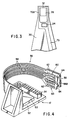
    The HSA 28 is provided, as shown in FIG. 2, with an arm 26 and a suspension 30 which has its base end fixed to the tip of the arm 26 by spot welding or bonding and extends from the arm. The arm 26 is formed from a stainless material, such as SUS304, into a planar plate which is small in thickness, of the order of 250 µm and is formed at its base end with a circular hole 31 into which the hub of the bearing assembly 18 is inserted. The suspension 30 is formed from an elongate plate spring having a thickness of 60 to 70 µm. The suspension 30 may be formed from the same material as the arm 26 so that they are integral with each other.
    The HSA 28 further includes a magnetic head 32 and a head IC 34 which are attached to the end of the suspension 30. The head 32 is a combined separate type of magnetic head which is constituted by a magneto-resistive element (hereinafter referred to as MR element) 321 adapted for reproducing (reading) as shown in FIGS. 5 to 9 and FIG. 11 and a thin-film head 322 adapted for recording (writing) as shown in FIGS. 7, 8 and 11. The head IC 34 is mounted in the form of a bare chip on the suspension 30.
    FIG. 3 shows the structure in which the MR head 32 and the head IC 34 are mounted on the suspension 30.
    As shown, the MR head 32 is installed in a substantially rectangular slider 36 fixed to a gimbal formed at the tip of the suspension 30. The slider 36 has the role to hold the head 32 above the surface of the rotating disk 12 so as to keep a constant distance from the surface of the rotating disk 12.
    On the other hand, the head IC 34 is mounted in the position closer to the arm 26 as viewed from the slider 36. That is, the head IC and the MR head are mounted on opposite sides of the slider.
    The head 32 and the head IC 34 mounted on the suspension 30 of the HSA 28 are electrically connected together by a pattern of interconnections formed on a relay flexible printed circuit board (hereinafter referred to as relay FPC) 70 as a cabling member. The relay FPC 70 is attached to the surfaces of the arm 26 and the suspension 30 of the HSA 28 with adhesive so as to extend from the tip of the suspension 30 to the base end of the arm 26 as shown in FIG. 2.
    The relay FPC 70 is shaped into an elongate stripe form as a whole and has a tip portion 70a positioned at the tip of the suspension 30 and a soldering portion (connecting portion) 70b derived from the base end of the arm 26. The tip portion 70a is formed with electrode pads (not shown) which are electrically connected with the electrodes of the MR head 32 and the electrodes of the head IC 34. The soldering portion 70b has six electrode pads 72.
    That portion of the relay FPC 70 which corresponds to the base end side of the arm 26 is bent substantially at right angles, forming the bent portion 82. Thus, the soldering portion 70b of the relay FPC 70 extends at right angles with respect to the surface of the arm 26 and in parallel with an extending end portion 56a of the main FPC 56 fixed to the bearing assembly 18.
    Referring back to FIG. 1, the board unit 17 has a rectangular board 52 fixed to the bottom of the housing 10, which has electronic components including a control IC 53 and a connector 54 mounted on it.
    The board unit 17 has a main flexible printed circuit board (hereinafter referred to as main FPC) 56 in the form of a strip that connects the head ICs 34 of the HSAs 28 to the board 52 through the relay FPCs 70.
    The main FPC 56 is drawn from the board 52 as shown in FIG. 4. A reinforcing plate 50 is attached to the rear side of the leading portion 56a of the main FPC 56. A pair of holes 64 is formed in the leading portion 56a. The leading portion 56a is screwed through the holes 64 into to the bearing assembly 18 of the carriage assembly 14. The main FPC 56 is formed integral with the board 52 by the flexible printed circuit board.
    A pattern of interconnections 58 is formed on the main FPC 56 which extend in parallel with one another along the axial direction of the main FPC 56. The leading portion 56a of the main FPC 56 is formed with six sets of connection pad portions 60 in correspondence with the number of the heads 32. In this embodiment, each connection pad portion 60 comprises six connection pads 62, which are arranged in a line at regular intervals along the axial direction of the main FPC 56. The connection pad portions 60 are arranged in parallel with one another with space between them in the direction perpendicular to the axial direction of the main FPC 56.
    The six connection pads 62 in each connection pad portion 60 are electrically connected with the board 52 through the pattern of interconnections 58.
    The soldering portion 70b of the relay FPC 70 extending from the suspension 30 of each HSA 30 to the corresponding arm 26 is electrically and mechanically connected with the leading portion 56a of the main FPC 56 by soldering each of the six connection pads 72 and a corresponding one of the six connection pads 62 in the corresponding set of connection pads on the main FPC 56 side.
    Next, the arrangement of the head IC 34 mounted on the suspension 30 of the HSA 28 will be described with reference to FIGS. 5 through 8. Four arrangements of the head IC are described herein.
    [First Arrangement of Head IC]
    In FIG. 5, there is illustrated, in block diagram form, a first arrangement of the head IC 34.
    The head IC 34 has a first MR terminal 101, a second MR terminal 102, a first power supply terminal 105, a second power supply terminal 106, a bias current terminal 107, and a read output terminal 108.
    The head IC 34 has an MR protection circuit 201, a differential input type of read amplifier circuit 202, and a resistor 203 built in. The MR protection circuit 201 is adapted to protect the MR element 321 in the MR head 32 from electrostatic breakdown, and the resistor 203 serves as an adjust circuit for balancing (adjusting) the input impedance of the read amplifier circuit 202.
    It should be noted here that the head IC 34 of FIG. 5 has no write driver circuit built in. The write driver circuit is formed in the control IC 53 (see FIG. 11) mounted on the board unit 17 shown in FIGS. 1 and 4.
    To the first and second MR terminals 101 and 102 of the head IC 34 are connected both ends of the MR element 321 of the MR head 32. To the first and second power supply terminals 105 and 106, the bias current terminal 107 and the read output terminal 108 is connected the control IC 53 on the board unit 17 through the relay FPC 70 and the main FPC 56. Though not shown in FIG. 5, the two terminals (electrodes) of the thin-film head 322 for writing are directly connected to the control IC 53 through the relay FPC 70 and the main FPC 56 with no head IC involved.
    A total of six head ICs 34 mounted on the suspensions 30 of the HSAs 28 and the control IC 53 mounted on the board unit 17 form the head amplifier circuit. That is, this embodiment is characterized in that the function of the head amplifier circuit is shared between the suspensions 30 of the HSAs 28 and the board units 17.
    In the head IC 34 forming a part of the head amplifier circuit, the first and second MR terminals 101 and 102 are connected through the MR protection circuit 201 to the read amplifier circuit 202, which has its output connected to the read output terminal 108.
    As is evident from the above description, this embodiment is arranged such that the head ICs 34 forming part of the head amplifier circuit are mounted on the suspensions 30 of the HSAs 28 not on the board unit 17 and the MR protection circuit 201 is built into each head IC 34. For this reason, even if ESD (electrostatic discharge) occurs in the vicinity of the soldering portion 70b through the worker when he or she is soldering the electrode pads 72 in the soldering portion of the relay FPC 70 and the electrode pads 62 of the main FPC 56, the MR protection circuit 201 in the head IC 34 installed between the soldering portion and the MR element 321 of the MR head 32 effectively functions to protect the MR element 321 from electrostatic breakdown.
    If the MR protection circuit were built into the head amplifier circuit provided on the board unit 17 side as hitherto, the occurrence of ESD during soldering would cause discharge current due to ESD to flow in the MR element independently of the MR protection circuit, destroying the MR element.
    In this embodiment, the function of the head amplifier circuit is shared between the suspensions 30 of the HSAs 28 and the board unit 17, which, as will be described hereinafter, helps reduce the number of interconnections for connecting the head ICs 34 which correspond in number to the MR heads 32 (six in this example) with the control IC 53.
    In the head IC 34 of FIG. 5, a supply voltage is supplied from the control IC 53 over the main FPC 56 and the relay FPC 70 to the first and second power supply terminals 105 and 106, where a positive power is supplied to the first power supply terminal 105 and a negative power (or ground level) is supplied to the second power supply terminal 106.
    The bias current terminal 107 of the head IC 34 is supplied with a bias current from the control IC 53 through the main FPC 56 and the relay FPC 70. This bias current is supplied to the MR element 321 through the MR protection circuit 201 and the first MR terminal 101 and then returns to a second power supply V2 at the negative or ground level through the second MR terminal 102, the MR protection circuit 201, and the resistor 203.
    When a bias current is supplied from the head IC 34 to the MR element 321, data recorded on a track of the disk 12 (see FIG. 1) over which the MR element 321 of the MR head 32 is currently positioned is read (reproduced). The signal (read signal) read by the MR element 321 is conducted through the first and second MR terminals 101 and 102 and the MR protection circuit 201 to the read amplifier circuit 202. The signal amplified by the read amplifier circuit 202 is output to the read output terminal 108. The appropriate setting of the value of the resistor 203 allows the differential input impedance of the read amplifier circuit 202 to be balanced, allowing the read signal to be amplified with precision.
    The read signal output from the read amplifier circuit 202 to the read output terminal 108 is sent to the control IC 53 through the relay FPC 70 and the main FPC 56.
    At the time of writing, on the other hand, a write current from the write driver circuit 205 (see FIG. 11) in the control IC 53 is directly supplied to the thin-film head 322 via the main FPC 56 and the relay FPC 70 without passing through the head IC 34.
    By using the head IC arranged described above, this embodiment, it becomes possible to not only efficiently prevent the MR head 32 by the MR protection circuit 201 from suffering electrostatic breakdown during the assembly process of incorporating the HSA 28 into the disk drive unit as described previously, but also allow the number of interconnections formed on the relay FPC 70 attached to the arm 26 and the suspension 30 of the HSA 28, i.e., the number of electrode pads 72 of the soldering portion 70b, to be six in total; four for the first power supply V1, the second power supply V2, the bias current, and the read signal (read output signal), and two for connection to the thin-film head 25. That is, this embodiment requires addition of only two interconnections in comparison with the case where no head IC 34 is mounted on the HAS 28. Thus, an increase in soldering cost resulting from mounting the head IC 34 on the HSA 28 can be minimized. In addition, the formation of the electrode pads 72 on the relay FPC 70 is kept from becoming difficult.
    Furthermore, the incorporation of the read amplifier circuit 202 into the head IC 34 not into the control IC 53 on the board unit 17 side, i.e., the placement of the read amplifier circuit in the vicinity of the MR head 32 allows noise occurring in the interconnections between the MR head 32 and the read amplifier circuit 202 to be decreased significantly, implementing high-density recording based on the MR head 32.
    [Second Arrangement of Head IC]
    A second arrangement of the head IC 28 mounted on the suspension of the HSA 28 will be described with reference to FIG. 6, in which like reference numerals are used to denote corresponding components to those in FIG. 5.
    The head IC 34 of FIG. 6 is characterized in that, as the adjust circuit for balancing the input impedance of the read amplifier circuit 202, a constant current circuit 204 is used instead of the resistor 203 used in the arrangement of FIG. 5.
    In the arrangement of FIG. 6, the MR element 321 has its ends connected through the first and second MR terminals 101 and 102 and the MR protection circuit 201 to the read amplifier circuit 202. The read amplifier circuit 202 amplifies a read signal from the MR element 321 and provides the amplified read signal to the output terminal 108. The bias current terminal 107 is supplied with a bias current from the control IC 53 over the main FPC 56 and the relay FPC 70. This bias current is supplied to the MR element 321 through the MR protection circuit 201 and the first MR terminal 101 and then returns to the second power supply V2 through the second MR terminal 102, the MR protection circuit 201, and the constant current source 204. The supply voltage is supplied from the control IC 53 through the main FPC 56, the relay FPC 70, and the first and second power supply terminals 105 and 106.
    In this arrangement, as in the first arrangement, the MR head 32 is efficiently prevented by the MR protection circuit 201 from suffering electrostatic breakdown during the assembly process of incorporating the HSA 28 into the disk drive unit, and the number of electrode pads 72 of the soldering portion 70b of the relay FPC 70 is allowed to be six in total; four for the first power supply V1, the second power supply V2, the bias current, and the read output signal, and two for connection to the thin-film head 25. Moreover, noise occurring in the interconnections between the MR head 32 and the read amplifier circuit 202 can be reduced significantly. Furthermore, using the constant current circuit 204 instead of the resistor 203 allows the input impedance of the read amplifier circuit 202 to be balanced better than in the case where the resistor 203 is used.
    [Third Arrangement of Head IC]
    A third arrangement of the head IC 34 mounted on the suspension of the HSA 28 will be described with reference to FIG. 7, in which like reference numerals are used to denote corresponding components to those in FIG. 6.
    Unlike the head IC of FIG. 6, in the head IC 34 of FIG. 7, the read amplifier circuit 202 is not built in, but a write driver circuit 205 and a write current circuit 206 are built in instead. In this case, unlike the previous example, the control IC 53 has the read amplifier circuit 202 built in but has no write driver circuit 205 and write current circuit 206 built in.
    The head IC 34 of FIG. 7 has a first MR terminal 101, a second MR terminal 102, a first power supply terminal 105, a second power supply terminal 106, a bias current terminal 107, a read output terminal 108, a write current setting terminal 109, and a write data terminal 110.
    The head IC 34 has an MR protection circuit 201 for protecting the MR element 321 from electrostatic breakdown, a constant current circuit 204, a write driver circuit 205, and a write current circuit 206 built in.
    Both ends of the MR element 321 of the MR head 32 are connected to the first and second MR terminals 101 and 102 of the head IC 34. Likewise, both ends of a thin-film head 322 of the MR head 32 are connected to first and second thin- film terminals 103 and 104. To the first and second power supply terminals 105 and 106, the bias current terminal 107, the read output terminal 108, the write current setting terminal 109 and the write data terminal 110 is connected the control IC 53 on the board unit 17 through the relay FPC 70 and the main FPC 56.
    In the head IC 34 of FIG. 7, a supply voltage is supplied from the control IC 53 through the main FPC 56 and the relay FPC 70 to the first and second power supply terminals 105 and 106, where a positive power is supplied to the first power supply terminal 105 and a negative power (or ground level) is supplied to the second power supply terminal 106.
    Moreover, in the head IC 34 of FIG. 7, the bias current terminal 107 of the head IC 34 is supplied with a bias current from the control IC 53 over the main FPC 56 and the relay FPC 70. This bias current is supplied to the MR element 321 through the MR protection circuit 201 and the first MR terminal 101 and then returns to a second power supply V2 through the second MR terminal 102, the MR protection circuit 201, and the constant current circuit 204. The constant current circuit 204 may be replaced with the resistor 203 shown in FIG. 5.
    A read signal from the MR element 321 is conducted through the first and second MR terminals 101 and 102 and the MR protection circuit 201 to the bias current terminal 107 and the read output terminal 108. The read signal conducted through the first and second MR terminals 101 and 102 is then sent to the read amplifier circuit in the control IC 53 over the relay FPC 70 and the main FPC 56.
    At the time of writing of data, on the other hand, write current is supplied to the thin-film head 322 from the write driver circuit 205 that reverses the direction of current flow at the edges of a write data signal from the write data terminal 110, so that data is written (recorded) onto a track of the disk 12 (see FIG. 1) over which the thin-film head 322 of the MR head 32 is positioned. The value of a current supplied from the write driver circuit 205 to the thin-film head 322 is determined by the write current circuit 206 in accordance with a voltage signal supplied from the control IC 53 over the main FPC and the relay FPC to the write current setting terminal 109.
    By using the head IC 34 arranged described above, this embodiment, it becomes possible to not only efficiently prevent the MR head 32 by the MR protection circuit 201 from suffering electrostatic breakdown during the assembly process of incorporating the HSA 28 into the disk drive unit, but also allow the number of interconnections formed on the relay FPC 70 attached to the arm 26 and the suspension 30 of the HSA 28, i.e., the number of electrode pads 72 of the soldering portion 70b, to be six in total; for the first power supply V1, the second power supply V2, the bias current, the read signal (read output signal), the write data, and the write current setting signal. That is, this embodiment requires addition of only two interconnections in comparison with the case where no head IC is mounted on the HAS 28. Thus, an increase in soldering cost resulting from mounting the head IC 34 on the side of the HSA 28 can be minimized. In addition, the formation of the electrode pads 72 on the relay FPC 70 is kept from becoming difficult.
    Furthermore, the incorporation of the write driver circuit 205 into the head IC 34 not into the control IC 53 of the board unit 17 reduces the distance between the write driver circuit 205 and the MR head 32, allowing inductance of the interconnections on the relay FPC 70 between the MR head 32 and the write driver circuit 205 to be reduced and thus allowing the write current to the head to rise and fall quickly. High-density recording can therefore be accomplished.
    [Fourth Arrangement of Head IC]
    A fourth arrangement of the head IC 34 mounted on the suspension of the HSA 28 will be described with reference to FIG. 8, in which like reference numerals are used to denote corresponding components to those in FIG. 6.
    The head IC 34 of FIG. 8 is characterized by addition of the write driver circuit 205, the write current circuit 206, the write current setting terminal 109, and the write data terminal 110 shown in FIG. 7 to the arrangement of FIG. 6.
    The bias current terminal 107 of the head IC 34 is supplied with a bias current from the control IC 53 over the main FPC 56 and the relay FPC 70. This bias current is supplied to the MR element 321 through the MR protection circuit 201 and the first MR terminal 101 and then returns to the second power supply V2 through the second MR terminal 102, the MR protection circuit 201, and the constant current circuit 204. The constant current circuit 204 may be replaced with the resistor 203 shown in FIG. 5.
    A read signal from the MR element 321 is conducted through the MR protection circuit 201 to the read amplifier circuit 202 and then output to the read output terminal 108. The read signal amplified by the read amplifier circuit 202 is then sent to the control IC 53 over the relay FPC 70 and the main FPC 56.
    At the time of writing of data, on the other hand, write current is supplied to the thin-film head 322 from the write driver circuit 205 that reverses the direction of current flow at the edges of a write data signal from the write data terminal 110, so that data is written (recorded) onto a track of the disk 12 (see FIG. 1) over which the thin-film head is positioned. The value of a current supplied from the write driver circuit 205 to the thin-film head 322 is determined by the write current circuit 206 in accordance with a voltage signal supplied from the control IC 53 over the main FPC 56 and the relay FPC 70 to the write current setting terminal 109.
    Therefore, like the third arrangement, the head IC 34 of FIG. 8 allows the MR protection circuit 201 to efficiently prevent the MR head 32 by the MR protection circuit 201 from suffering electrostatic breakdown during the assembly process of HSA 28 and allows the number of electrode pads 72 of the soldering portion 70b of the relay FPC 70 attached to the arm 26 and the suspension 30 of the HSA 28 to be six in total; for the first power supply V1, the second power supply V2, the bias current, the read signal (read output signal), the write data, and the write current setting signal.
    Furthermore, the incorporation of the read amplifier circuit 202 and the write driver circuit 205 into the head IC 34 not into the control IC 53 reduces the distance between the write driver circuit 205/read amplifier circuit 202 and the MR head 32, allowing noise occurring in interconnections on the relay FPC 70 between the MR head and the read amplifier circuit to be reduced and allowing inductance of the interconnections on the relay FPC 70 between the thin-film head 322 of the MR head 32 and the write driver circuit 205 to be reduced to thereby cause the write current to the head to rise and fall quickly. High-density recording can therefore be accomplished.
    [Fifth Arrangement of Head IC]
    A fifth arrangement of the head IC 34 mounted on the suspension of the HAS 28 will be described with reference to FIG. 9, in which like reference numerals are used to denote corresponding components to those in FIG. 6.
    The head IC 34 of FIG. 9 is characterized by replacing the bias current terminal 107 of FIG. 6 with a bias current setting terminal 111 for receiving an externally supplied bias current setting signal for setting the bias current value and adding a bias current amplifier circuit 207 for producing a bias current having a value determined by the bias current setting signal.
    In the head IC 34 of FIG. 9, the bias current setting terminal 111 is supplied with the bias current setting signal from the control IC 53 over the main FPC 56 and the relay FPC 70. The bias current amplifier 207 produces a bias current the value of which depends on the bias current setting signal. This bias current is supplied to the MR element 321 through the MR protection circuit 201 and the first MR terminal 101 and then returns to the second power supply V2 through the second MR terminal 102, the MR protection circuit 201, and the constant current circuit 204. The constant current circuit 204 may be replaced with the resistor 203 shown in FIG. 5.
    A read signal from the MR element 321 is conducted through the MR protection circuit 201 to the read amplifier circuit 202 and then output to the read output terminal 108. The read signal amplified by the read amplifier circuit 202 is then sent to the control IC 53 through the relay FPC 70 and the main FPC 56.
    The write driver circuit 205, the write current circuit 206, the write current setting terminal 109 and the write data terminal 110 shown in FIGS. 7 and 8 may be added to the arrangement of FIG. 9.
    With this arrangement, as in the first arrangement, the MR head 32 is efficiently prevented by the MR protection circuit 201 from suffering electrostatic breakdown during the assembly process of incorporating the HSA 28 into the disk drive unit, and the number of electrode pads 72 of the soldering portion 70b of the relay FPC 70 is allowed to be six in total; four for the first power supply V1, the second power supply V2, the bias current, and the read output signal, and two for connection to the thin-film head 25. Moreover, noise occurring in the interconnections between the MR head 32 and the read amplifier circuit 202 can be suppressed significantly.
    Unlike the first arrangement, in the fifth arrangement, the bias current setting terminal 111 is provided instead of the bias current terminal 107 and the bias current amplifier circuit 207 is provided to thereby allow the bias current amplifier circuit 207 to produce a bias current in accordance with a bias current setting signal externally supplied to the bias current setting terminal 111, thus making the bias current less susceptible to noise.
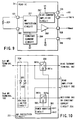
    [Arrangement of MR Protection Circuit 201]
    Hereinafter, an arrangement of the MR protection circuit 201 built into the head IC 34 which is mounted on the suspension 30 and arranged as shown in FIG. 5, 6, 7, 8, or 9 will be described with reference to FIG. 10.
    The MR protection circuit 201 includes first and second switches 301 and 302 each of which is turned OFF while the power is not supplied and ON while the power is supplied, a power monitor circuit 303, and a voltage limiter circuit 304. One pole 301a of the first switch 301 is connected
    with the bias current terminal 107 of the head IC 34 (with the output of the bias current amplifier circuit 207 when the head IC 34 is arranged as shown in FIG. 9). The other pole 301b of the first switch 301 is connected to the first MR terminal 101 of the head IC 34 and to one input of the read amplifier circuit 202 built into the head IC 34 (when it is arranged as shown in FIG. 5, 6, 8, or 9) or one input of the read amplifier circuit 202 built into the control IC 53 (when the head IC 34 is arranged as shown in FIG. 7).
    Thus, the first switch 301, when turned ON, supplies a bias current from the bias current terminal 107 (from the bias current amplifier circuit 207 when the head IC 34 is arranged as shown in FIG. 9) to the MR element 321 shown in FIGS. 5 to 9 through the first MR terminal 101.
    On the other hand, one pole 302a of the second switch 302 is connected either to the resistor 203 (when the head IC 34 is arranged as shown in FIG. 5) or to the constant current circuit 204 (when the head IC 34 is arranged as shown in FIGS. 6 to 9). The other pole 302b of the second switch 302 is connected to the read amplifier circuit 202 built in the head IC 34 (when the head IC 34 is arranged as shown in FIG. 5, 6, 8, or 9) or to the read amplifier circuit 202 built in the control IC 53 (when the head IC 34 is arranged as shown in FIG. 7), and to the second MR terminal 102 of the head IC 34.
    Thus, the second switch 302 allows the bias current supplied to the MR element 321 through the first MR terminal 101 to flow through the MR element 321 and then return to the second power supply terminal 106 at V2 through the second MR terminal 102 and the resistor 203 or the constant current source 204.
    The first and second switches 301 and 302 are subjected to ON/OFF control by the power monitor circuit 303. That is, the power monitor circuit 303 monitors the power supplies V1 and V2 and, when V1 and V2 reach predetermined levels or in predetermined ranges, turns ON the first and second switches 301 and 302. In other words, when the power is OFF, the first and second switches 301, 302 are turned OFF. In the assembly process of HSA 28 during which the power is OFF, therefore, the MR protection circuit 201 in the head IC 34 provides isolation between the MR head 32 and the soldering portion 70b of the relay FPC 70 of the HSA 28, so that, even if ESD occurs in the vicinity of the soldering portion 70b through the worker, the MR element 321 can be protected from electrostatic breakdown. If the MR protection circuit 201 were provided on the side of the board unit 17, then such an effect would not be provided.
    In the MR protection circuit 201, a voltage limiter circuit 304 is connected between the pole 301b of the first switch 301 and the pole 302b of the second switch 302, which has a pair of diodes 305 and 306 connected in parallel with opposite polarity. For this reason, even if ESD occurs for some cause while the power is supplied and hence the first and second switches 301, 302 are placed in the ON state, the voltage between the first and second MR terminals 101 and 102 will not exceed a constant voltage determined by the backward characteristic of the diodes 304 and 305, thus protecting the MR element 321 connected between the first and second MR terminals 101 and 102 from electrostatic breakdown.
    [Arrangement of Control IC 53]
    Next, an arrangement of the control IC 53 mounted on the board unit 17 will be described with reference to FIG. 11 taking, as an example, the case where the MR protection circuit 210 and the read amplifier circuit 202 are built into the head IC 34 as shown in FIG. 5 and the write driver circuit 205 is built into the control IC 53.
    Into the control IC 53 are built a head switching circuit 410, a bias current circuit 420, a buffer amplifier circuit 430, a write current circuit 206, a serial/logic control circuit 440, a power ON/OFF circuit 450, and a fault/safe circuit 460.
    The head switching circuit 410 in the control IC 53 includes write driver circuits 205 and operational circuits 411, which correspond in number to the MR heads 32. At the time of reading, the head switching circuit 410 supplies the bias current terminal 107 (see FIG. 5) of the head IC 34 corresponding to the MR element 321 of a selected MR head 32 with a bias current the value of which is set by the bias current circuit 420 as a constant current circuit.
    The bias current supplied from the head switching circuit 410 to the head IC 34 is supplied to the corresponding MR element 321 through the MR protection circuit 201 in the head IC 34 (see FIG. 5). Thereby, data is read by the MR element 321 and the resulting read signal is amplified by the read amplifier circuit 202 (see FIG. 5) in the head IC 34.
    The read signal read from the MR element 321 and amplified by the read amplifier circuit 202 in the head IC 34 is output from the read output terminal 108 (see FIG. 5) of the head IC 34 and then input to the corresponding operational amplifier circuit 411 in the control IC 53. The operational amplifier circuit 411 amplifies AC components contained in the read signal amplified by the read amplifier circuit 202 in the head IC 34. The read signal amplified by the operational amplifier circuit 411 is sent through the buffer amplifier circuit 430 to a read/write IC (read/write channel) not shown as read data signals RDX and RDY, where they are decoded into NRZ code data by way of example.
    At the time of writing, the head switching circuit 410 switches the direction of current set by the write current circuit 206 at the edges of write data signals WDX and WDY from the read/write IC by the write driver circuit 205 corresponding to the thin-film head 322 of a selected MR head 32 and then supplies the write current to the corresponding thin-film head 322.
    The serial/logic control circuit 440 is connected to a serial port 441 for serial data SDATA, a serial data enable signal SDEN representing the timing of serial transfer, and a shift clock SCLK and a signal R/XW for specifying either of disk read and disk write modes. The serial/logic control circuit 440 is responsive to control signals supplied thereto under the control of a CPU (not shown) and the signal R/XW to perform the selection of a head, the setting and ON/OFF control of the bias current, the setting and ON/OFF control of the write current, the control of the power ON/OFF circuit 450, and the control of the fault/safe circuit 460.
    The write current circuit 206 is responsive to a control signal from the serial/logic control circuit 440 to set the write current, which, in turn, is supplied to the write driver circuit 205 corresponding to a selected MR head 32.
    The bias current circuit 420 is responsive to a control signal from the serial/logic circuit 440 to set the bias current. The set bias current is supplied from the head switching circuit 410 to the head IC 34 corresponding to a selected MR head 32.
    The fault/safe circuit 460 is adapted to test each MR head. The circuit 460 is responsive to a control signal from the serial/logic control circuit 440 to switch between read and write modes and make a selection from the MR heads 32 and outputs a fault signal representing an abnormality of a selected MR head 32 when signals from the corresponding head IC 32 are abnormal.
    Although a description was made of the control IC 53 when the head IC 34 is arranged as shown in FIG. 5, the control IC 53 can be configured likewise even when the head IC 34 is arranged as shown in any one of FIGS. 6 to 9. When the head IC 34 is arranged as shown in FIG. 7, the control IC 53 is arranged such that the read amplifier circuit 202 is connected to the input of each of the operational amplifier circuits 411 in the head switching circuit 410 and the write driver circuits 205 and the write current circuit 206 are removed. When the head IC 34 is arranged as shown in FIG. 8, it is only required to remove the write driver circuits 205 and the write current circuit 206 from the control IC 53. When the head IC 34 is arranged as shown in FIG. 9, that is, when the head IC 34 is equipped with the bias current amplifier circuit 207, it is only required to remove the bias current circuit 420 from the control IC 53.
    Although, in the embodiments described so far, the relay FPC 70 as a flexible interconnection board is used for electrical connections between the MR head 32 and the head IC 34 and between the head IC 34 and the control IC 53 through the main FPC 56, conductor cables may be used instead.
    According to the present invention, as described above, an integrated circuit device (head IC) having a built-in MR protection circuit for protecting an MR head composed of an MR element for reading and a thin-film head for writing from electrostatic breakdown, is mounted on a suspension that supports the MR head, so that the built-in MR protection circuit effectively functions to avoid electrostatic breakdown even if ESD occurs during the assembly process of incorporating the HSA into the disk drive unit.
    According to the present invention, the incorporation of a read amplifier circuit into the head IC mounted on the HSA suspension reduces the distance between the MR head and the read amplifier circuit, thus suppressing noise occurring in interconnections between the magnetic head and the read amplifier circuit and allowing the MR head to display its performance fully for high-density recording.
    According to the present invention, the incorporation of a write driver circuit into the head IC mounded on the HSA suspension reduces the distance between the MR head and the write driver circuit, thus reducing inductance associated with interconnections between the magnetic head and the write driver circuit and allowing the write characteristics to be improved.
    According to the present invention, even when a head IC is mounted on the HSA suspension and an MR protection circuit and at least one of a read amplifier circuit and a write driver circuit are incorporated into the head IC, the number of interconnections extending from the HSA is allowed to be six in total, thus checking an increase in the soldering cost.

    Claims (19)

    1. A head suspension assembly (28) characterized by comprising:
      a magnetic head (32) constituted by a magnetoresistive element (321) for reading data and a head element (322) for writing data;
      a slider (36) for holding the magnetic head (32) above a surface of a rotating magnetic recording medium (12);
      a suspension (30) for supporting the slider (36); and
      a head integrated circuit (34) mounted on the suspension (30), the head integrated circuit (34) including a built-in protection circuit (201), electrically connected with the magnetoresistive element (321), for protecting the magnetoresistive element (321) from electrostatic breakdown.
    2. The head suspension assembly (28) according to claim 1, characterized in that the head IC (34) includes at least one of a read amplifier circuit (202) for amplifying a read signal read by the magneto-resistive element (321) from the magnetic recording medium (12) and a write driver circuit (205) for supplying the writing head element (322) with a write current corresponding to a write data signal.
    3. A head amplifier circuit for use in a magnetic disk drive including a head suspension assembly (28) having a magnetic head (32) constituted by a magneto-resistive element (321) for reading data and a head element (322) for writing data, a slider (36) for holding the magnetic head (32) above a surface of a rotating magnetic recording medium (12), and a suspension (30) for supporting the slider (36), the
      head amplifier circuit characterized by comprising: a head IC (Integrated Circuit) (34) mounted on the suspension (30), the head IC (34) including a built-in protection circuit (201), electrically connected with the magnetoresistive element (321), for protecting the magnetoresistive element (321) from electrostatic breakdown; and
      a control IC (53) for controlling the head IC (34).
    4. The head amplifier circuit according to claim 3, characterized in that the head IC (34) includes at least one of a read amplifier circuit (202) for amplifying a read signal read by the magneto-resistive element (321) from the magnetic recording medium (12) and a write driver circuit (205) for supplying the writing head element (322) with a write current corresponding to a write data signal.
    5. A head IC (Integrated Circuit) (34) for use in a magnetic disk drive including a head suspension (30) assembly (28) having a magnetic head (32) constituted by a magnetoresistive element (321) for reading data and a head element (322) for writing data, a slider (36) for holding the magnetic head (32) above a surface of a rotating magnetic recording medium (12), and a suspension (30) for supporting the slider (36), the head IC (34) being mounted on the suspension (30), the head IC (34) characterized by comprising:
      first and second MR terminals (101, 102) connected to both ends of the magnetoresistive element (321);
      a bias current terminal (107) connected to receive an externally supplied bias current; and
      a protection circuit (201), connected with the first and second MR terminals (101, 102) and the bias current terminal (107), for protecting the magneto-resistive element (321) from electrostatic breakdown.
    6. The head IC (34) according to claim 5, characterized by further comprising:
      a read amplifier circuit (202) for amplifying a read signal read by the magnetoresistive element (321) from the magnetic recording medium (12).
    7. The head IC (34) according to claim 6, characterized by further comprising:
      an adjust circuit (203 or 204), connected between the protection circuit (201) and a ground or negative power supply terminal (V2), for adjusting an input impedance of the read amplifier circuit (202).
    8. The head IC (34) according to claim 7, characterized in that the adjust circuit (203 or 204) includes one of a resistor (203) and a constant current source (204).
    9. The head IC (34) according to claim 5, characterized by further comprising:
      a write driver circuit (205) for supplying the writing head element (322) with a write current corresponding to a write data signal.
    10. The head IC (34) according to claim 9, characterized by further comprising:
      a write current circuit (206) for setting a value of the write current supplied from the write driver circuit (205) to the writing head element (322) in accordance with an externally supplied voltage signal.
    11. The head IC (34) according to claim 5, characterized by further comprising:
      a read amplifier circuit (202), connected with the protection circuit (201), for amplifying a read signal read by the magnetoresistive element (321) from the magnetic recording medium (12); and
      a write driver circuit (205) for supplying the writing head element (322) with a write current corresponding to a write data signal.
    12. The head IC (34) according to claim 5, characterized in that the protection circuit (201) includes:
      a first switch circuit (301) for connecting/ disconnecting one of the first and second MR terminals (101, 102) to/from the bias current terminal (107); and
      a second switch circuit (302) for connecting/ disconnecting the other of the first and second MR terminals (101, 102) to/from a ground or negative power supply terminal (V2).
    13. The head IC (34) according to claim 12, characterized in that the protection circuit (201) includes a voltage limiter circuit (306), connected between the first and second MR terminals (101, 102), for limiting a voltage between the first and second MR terminals (101, 102) to a constant value or less.
    14. The head IC (34) according to claim 12, characterized in that each of the first and second switch circuits (301, 302) is placed in a disconnected state while power is not supplied and in a connected state while power is supplied.
    15. The head IC (34) according to claim 5, characterized by further comprising:
      a bias current amplifier circuit (207), connected between the protection circuit (201) and the bias current terminal (107), for amplifying a bias current supplied from the bias current terminal (107).
    16. The head IC (34) according to claim 15, characterized in that the protection circuit (201) includes:
      a first switch circuit (301) for connecting/ disconnecting one of the first and second MR terminals (101, 102) to/from the bias current amplifier circuit (207), and
      a second switch circuit (302) for connecting/ disconnecting the other of the first and second MR terminals (101, 102) to/from a ground or negative power supply terminal (V2).
    17. The head IC (34) according to claim 16, characterized in that the protection circuit (201) includes a voltage limiter circuit (306), connected between the first and second MR terminals (101, 102), for limiting a voltage between the first and second MR terminals (101, 102) to a constant value or less.
    18. A magnetic disk drive equipped with a head suspension assembly (28), the head suspension assembly (28) characterized by comprising:
      a magnetic head (32) constituted by a magnetoresistive element (321) for reading data and a head element (322) for writing data;
      a slider (36) for holding the magnetic head (32) above a surface of a rotating magnetic recording medium (12);
      a suspension (30) for supporting the slider (36); and
      a head integrated circuit (34) mounted on the suspension (30) and including a built-in protection circuit (201), electrically connected with the magnetoresistive element (321), for protecting the magnetoresistive element (321) from electrostatic breakdown.
    19. The magnetic disk drive according to claim 18, characterized by further comprising:
      a control integrated circuit (53) for forming a head amplifier circuit in combination with the head integrated circuit (34) and controlling the head integrated circuit (34).
    EP99117052A 1998-12-25 1999-08-30 Head IC, head amplifier circuit, head suspension assembly, and magnetic disk drive for avoiding electrostatic breakdown of magnetic head Withdrawn EP1014342A3 (en)

    Applications Claiming Priority (2)

    Application Number Priority Date Filing Date Title
    JP10369472A JP2000195023A (en) 1998-12-25 1998-12-25 Head suspension assembly and magnetic disk drive loading the same assembly
    JP36947298 1998-12-25

    Publications (2)

    Publication Number Publication Date
    EP1014342A2 true EP1014342A2 (en) 2000-06-28
    EP1014342A3 EP1014342A3 (en) 2002-12-11

    Family

    ID=18494513

    Family Applications (1)

    Application Number Title Priority Date Filing Date
    EP99117052A Withdrawn EP1014342A3 (en) 1998-12-25 1999-08-30 Head IC, head amplifier circuit, head suspension assembly, and magnetic disk drive for avoiding electrostatic breakdown of magnetic head

    Country Status (3)

    Country Link
    US (1) US6377411B1 (en)
    EP (1) EP1014342A3 (en)
    JP (1) JP2000195023A (en)

    Cited By (4)

    * Cited by examiner, † Cited by third party
    Publication number Priority date Publication date Assignee Title
    EP1045385A1 (en) * 1999-04-13 2000-10-18 Texas Instruments Incorporated Information recording and reproduction apparatus and disk drive
    EP1394778A1 (en) * 2001-05-25 2004-03-03 Fujitsu Limited Recording disk drive and head suspension assembly
    US9275665B2 (en) 2014-07-25 2016-03-01 HGST Netherlands B.V. Slider with high frequency voltage ground and low frequency DC voltage isolation
    CN111474991A (en) * 2020-03-08 2020-07-31 苏州浪潮智能科技有限公司 Device and method for fixing and damping hard disk based on electromagnetic field

    Families Citing this family (19)

    * Cited by examiner, † Cited by third party
    Publication number Priority date Publication date Assignee Title
    JP2001266511A (en) * 2000-03-24 2001-09-28 Toshiba Corp Head suspension assembly and magnetic disk unit provided with head suspension assembly
    US6608736B1 (en) * 2000-05-08 2003-08-19 International Business Machines Corporation Integrated trace suspension interconnect for high-data-rate single-ended preamplifier for (G)MR elements
    JP2002100016A (en) 2000-09-21 2002-04-05 Toshiba Corp Head suspension assembly
    JP3883037B2 (en) * 2001-02-28 2007-02-21 株式会社日立製作所 Medium recording / playback system
    US6775078B2 (en) * 2001-09-14 2004-08-10 Texas Instruments Incorporated Fast magneto-resistive head open and short detection for both voltage and current bias preamplifiers
    US6583968B1 (en) * 2001-10-31 2003-06-24 Western Digital Technologies, Inc. Spindle motor hub having equivalent MR read element bias voltage to mitigate potential between disk and MR read element
    US6891702B1 (en) 2002-10-31 2005-05-10 Western Digital Technologies, Inc. Method and devices for providing magnetoresistive heads with protection from electrostatic discharge and electric overstress events
    US7009820B1 (en) 2002-12-24 2006-03-07 Western Digital Technologies, Inc. Disk drive comprising depletion mode MOSFETs for protecting a head from electrostatic discharge
    US7595949B1 (en) * 2003-12-04 2009-09-29 Maxtor Corporation Method for active cancellation of write-to-read crosstalk
    US7119995B2 (en) * 2004-01-22 2006-10-10 Seagate Technology Llc ESD shunt for transducing head
    KR100604860B1 (en) * 2004-05-29 2006-07-31 삼성전자주식회사 Head protection circuit of hard disk drive
    US7005858B1 (en) 2004-09-23 2006-02-28 Hitachi Global Storage Technologies Netherlands, B.V. System and method for decreasing ESD damage during component level long term testing
    US7538986B2 (en) * 2004-11-10 2009-05-26 International Business Machines Corporation Multi-port cable for removable ESD/EOD protection for electronic devices
    US8169751B2 (en) 2006-06-27 2012-05-01 Hitachi Global Storage Technologies Netherlands B.V. Magnetoresistive sensor having a structure for activating and deactivating electrostatic discharge prevention circuitry
    US7804658B1 (en) * 2006-09-11 2010-09-28 Marvell International Ltd. Biasing RMR with constant power
    US8358202B2 (en) * 2006-12-26 2013-01-22 Semiconductor Energy Laboratory Co., Ltd. Semiconductor device
    US9159344B2 (en) 2013-05-08 2015-10-13 Western Digital Technologies, Inc. Disk drive read circuit comprising an AC coupled sense amplifier for amplifying a read signal
    US9047917B1 (en) 2013-11-26 2015-06-02 Western Digital Technologies, Inc. Disk drive slider with sense amplifier for coupling to a preamp through a supply/bias line and a read signal line
    US11496033B2 (en) * 2019-01-08 2022-11-08 Michael Boyd Device and method to generate and apply gravito-magnetic energy

    Citations (14)

    * Cited by examiner, † Cited by third party
    Publication number Priority date Publication date Assignee Title
    JPS58118017A (en) * 1981-12-29 1983-07-13 Seiko Epson Corp Magnetic head
    JPS58118016A (en) * 1981-12-29 1983-07-13 Seiko Epson Corp Magnetic head
    US5103353A (en) * 1990-05-01 1992-04-07 International Business Machines Corporation Low noise amplifier with short circuit protection for signals from magnetoresistive element
    US5357379A (en) * 1993-07-02 1994-10-18 Exar Corporation Read/write circuit with switchable head resistance for read and write modes
    US5430584A (en) * 1991-10-18 1995-07-04 International Microelectronic Products Disk drive interface combining a magneto-resistive read and inductive write circuits
    US5444579A (en) * 1993-12-17 1995-08-22 Imp, Inc. Preamplifier of a signal from a variable resistance sensor, and a current source
    US5452148A (en) * 1993-02-22 1995-09-19 Fujitsu Limited Preamplifing circuit for a magnetoresistance device
    US5559051A (en) * 1994-10-18 1996-09-24 International Business Machines Corporation Process for manufacturing a silicon chip with an integrated magnetoresistive head mounted on a slider
    WO1997009714A1 (en) * 1995-09-06 1997-03-13 Seagate Technology, Inc. Dynamically programmable magneto-resistive head write and read bias currents
    US5712747A (en) * 1996-01-24 1998-01-27 International Business Machines Corporation Thin film slider with on-board multi-layer integrated circuit
    US5790331A (en) * 1995-08-11 1998-08-04 Mitel Semiconductor Americas Inc. Current control circuit and method for programmable read write preamplifier
    US5831783A (en) * 1995-07-17 1998-11-03 Fujitsu Limited Power source control circuit for controlling an electric potential of a magnetic head and memory apparatus using such a power source control circuit
    US5831782A (en) * 1994-01-27 1998-11-03 Fujitsu Limited Method and apparatus for supplying optimal bias current to a magnetic head
    US5867888A (en) * 1996-10-08 1999-02-09 International Business Machines Corporation Magnetic head/silicon chip integration method

    Family Cites Families (3)

    * Cited by examiner, † Cited by third party
    Publication number Priority date Publication date Assignee Title
    JPH0670848A (en) 1992-08-26 1994-03-15 Toshiba Home Technol Corp Pot device
    US5748412A (en) * 1995-08-11 1998-05-05 Seagate Technology, Inc. Method and apparatus for protecting magnetoresistive sensor element from electrostatic discharge
    US5982569A (en) * 1997-08-15 1999-11-09 Texas Instruments Incorporated Read/write data interface and method of operation

    Patent Citations (14)

    * Cited by examiner, † Cited by third party
    Publication number Priority date Publication date Assignee Title
    JPS58118016A (en) * 1981-12-29 1983-07-13 Seiko Epson Corp Magnetic head
    JPS58118017A (en) * 1981-12-29 1983-07-13 Seiko Epson Corp Magnetic head
    US5103353A (en) * 1990-05-01 1992-04-07 International Business Machines Corporation Low noise amplifier with short circuit protection for signals from magnetoresistive element
    US5430584A (en) * 1991-10-18 1995-07-04 International Microelectronic Products Disk drive interface combining a magneto-resistive read and inductive write circuits
    US5452148A (en) * 1993-02-22 1995-09-19 Fujitsu Limited Preamplifing circuit for a magnetoresistance device
    US5357379A (en) * 1993-07-02 1994-10-18 Exar Corporation Read/write circuit with switchable head resistance for read and write modes
    US5444579A (en) * 1993-12-17 1995-08-22 Imp, Inc. Preamplifier of a signal from a variable resistance sensor, and a current source
    US5831782A (en) * 1994-01-27 1998-11-03 Fujitsu Limited Method and apparatus for supplying optimal bias current to a magnetic head
    US5559051A (en) * 1994-10-18 1996-09-24 International Business Machines Corporation Process for manufacturing a silicon chip with an integrated magnetoresistive head mounted on a slider
    US5831783A (en) * 1995-07-17 1998-11-03 Fujitsu Limited Power source control circuit for controlling an electric potential of a magnetic head and memory apparatus using such a power source control circuit
    US5790331A (en) * 1995-08-11 1998-08-04 Mitel Semiconductor Americas Inc. Current control circuit and method for programmable read write preamplifier
    WO1997009714A1 (en) * 1995-09-06 1997-03-13 Seagate Technology, Inc. Dynamically programmable magneto-resistive head write and read bias currents
    US5712747A (en) * 1996-01-24 1998-01-27 International Business Machines Corporation Thin film slider with on-board multi-layer integrated circuit
    US5867888A (en) * 1996-10-08 1999-02-09 International Business Machines Corporation Magnetic head/silicon chip integration method

    Non-Patent Citations (2)

    * Cited by examiner, † Cited by third party
    Title
    PATENT ABSTRACTS OF JAPAN vol. 007, no. 228 (P-228), 8 October 1983 (1983-10-08) & JP 58 118016 A (SUWA SEIKOSHA KK), 13 July 1983 (1983-07-13) *
    PATENT ABSTRACTS OF JAPAN vol. 007, no. 228 (P-228), 8 October 1983 (1983-10-08) & JP 58 118017 A (SUWA SEIKOSHA KK), 13 July 1983 (1983-07-13) *

    Cited By (6)

    * Cited by examiner, † Cited by third party
    Publication number Priority date Publication date Assignee Title
    EP1045385A1 (en) * 1999-04-13 2000-10-18 Texas Instruments Incorporated Information recording and reproduction apparatus and disk drive
    EP1394778A1 (en) * 2001-05-25 2004-03-03 Fujitsu Limited Recording disk drive and head suspension assembly
    US7050268B2 (en) * 2001-05-25 2006-05-23 Fujitsu Limited Disk drive with read IC chip and write IC chip mounted respectively on suspension and arm
    EP1394778A4 (en) * 2001-05-25 2007-09-05 Fujitsu Ltd Recording disk drive and head suspension assembly
    US9275665B2 (en) 2014-07-25 2016-03-01 HGST Netherlands B.V. Slider with high frequency voltage ground and low frequency DC voltage isolation
    CN111474991A (en) * 2020-03-08 2020-07-31 苏州浪潮智能科技有限公司 Device and method for fixing and damping hard disk based on electromagnetic field

    Also Published As

    Publication number Publication date
    US6377411B1 (en) 2002-04-23
    JP2000195023A (en) 2000-07-14
    EP1014342A3 (en) 2002-12-11

    Similar Documents

    Publication Publication Date Title
    US6377411B1 (en) Head IC, head amplifier circuit, head suspension assembly, and magnetic disk drive for avoiding electrostatic breakdown of magnetic head
    US6163443A (en) Actuator having MR element protecting means
    JP4076434B2 (en) Magnetic head and head gimbal assembly
    USRE37869E1 (en) Head signal supply/retrieval structure for magnetic disc drive
    US6967800B1 (en) Disk drive suspension assembly including a base plate with mass reduction openings at distal corners
    US7609482B2 (en) Magnetic head slider supporting device including conductor for reducing crosstalk between lines
    US7113372B2 (en) HGA plateau gimbal design
    US20050013051A1 (en) Head suspension assembly and magnetic disk apparatus comprising the head suspension assembly
    US6721135B2 (en) Printed circuit cable connector attachment assembly
    US7606003B2 (en) Electrical device for interconnecting magnetic head and driving circuit which uses adjusted length wires of opposite polarity to reduce crosstalk and storage apparatus including same
    US5909338A (en) Magnetic disk drive having a Z-shaped grounding portion in the flex circuit cable
    US5991121A (en) Head assembly having short circuit pattern short-circuiting a pair of lead lines
    KR100326628B1 (en) Head/suspension design having fewer signal wires and making the same
    US5905609A (en) Magnetic disk drive having a VCM plate which includes an elongated protrusion for securing a flex clamp to the base
    US20080080096A1 (en) Head slider supporting device and storage device
    US5963399A (en) Dual loop flex circuit for a linear actuator
    JP2007157209A (en) Magnetic recording device
    US11430474B1 (en) Hard disk drive suspension tail having narrowing tip
    CN115589662A (en) Flexible printed circuit finger layout for low crosstalk
    KR20070037857A (en) Slider, head gimbal assembly, and hard disc drive
    KR20000022669A (en) Head assembly and disk drive
    JPH1145423A (en) Magnetic head slider and magnetic head assembly
    KR100425469B1 (en) Electrical substrate and hard disk drive adopting the same
    KR100864402B1 (en) Hard disk drive
    US20050099721A1 (en) Magnetic disk drive apparatus and manufacturing method of magnetic disk drive apparatus

    Legal Events

    Date Code Title Description
    PUAI Public reference made under article 153(3) epc to a published international application that has entered the european phase

    Free format text: ORIGINAL CODE: 0009012

    17P Request for examination filed

    Effective date: 19990830

    AK Designated contracting states

    Kind code of ref document: A2

    Designated state(s): AT BE CH CY DE DK ES FI FR GB GR IE IT LI LU MC NL PT SE

    AX Request for extension of the european patent

    Free format text: AL;LT;LV;MK;RO;SI

    PUAL Search report despatched

    Free format text: ORIGINAL CODE: 0009013

    AK Designated contracting states

    Kind code of ref document: A3

    Designated state(s): AT BE CH CY DE DK ES FI FR GB GR IE IT LI LU MC NL PT SE

    AX Request for extension of the european patent

    Free format text: AL;LT;LV;MK;RO;SI

    AKX Designation fees paid

    Designated state(s): DE FR GB

    STAA Information on the status of an ep patent application or granted ep patent

    Free format text: STATUS: THE APPLICATION IS DEEMED TO BE WITHDRAWN

    18D Application deemed to be withdrawn

    Effective date: 20060102