EP1013454A1 - Thermal printing head - Google Patents
Thermal printing head Download PDFInfo
- Publication number
- EP1013454A1 EP1013454A1 EP98911150A EP98911150A EP1013454A1 EP 1013454 A1 EP1013454 A1 EP 1013454A1 EP 98911150 A EP98911150 A EP 98911150A EP 98911150 A EP98911150 A EP 98911150A EP 1013454 A1 EP1013454 A1 EP 1013454A1
- Authority
- EP
- European Patent Office
- Prior art keywords
- severable
- drive ics
- wiring
- conductor wirings
- main conductor
- Prior art date
- Legal status (The legal status is an assumption and is not a legal conclusion. Google has not performed a legal analysis and makes no representation as to the accuracy of the status listed.)
- Granted
Links
- 238000007651 thermal printing Methods 0.000 title 1
- 239000004020 conductor Substances 0.000 claims abstract description 58
- 238000011084 recovery Methods 0.000 claims abstract description 15
- 238000010438 heat treatment Methods 0.000 description 17
- 239000000758 substrate Substances 0.000 description 17
- 238000000034 method Methods 0.000 description 4
- 238000003754 machining Methods 0.000 description 3
- PNEYBMLMFCGWSK-UHFFFAOYSA-N Alumina Chemical compound [O-2].[O-2].[O-2].[Al+3].[Al+3] PNEYBMLMFCGWSK-UHFFFAOYSA-N 0.000 description 2
- 239000003822 epoxy resin Substances 0.000 description 2
- 229920000647 polyepoxide Polymers 0.000 description 2
- 230000000717 retained effect Effects 0.000 description 2
- 230000005540 biological transmission Effects 0.000 description 1
- 239000011248 coating agent Substances 0.000 description 1
- 238000000576 coating method Methods 0.000 description 1
- 230000003247 decreasing effect Effects 0.000 description 1
- 238000005530 etching Methods 0.000 description 1
- PCHJSUWPFVWCPO-UHFFFAOYSA-N gold Chemical compound [Au] PCHJSUWPFVWCPO-UHFFFAOYSA-N 0.000 description 1
- 238000004519 manufacturing process Methods 0.000 description 1
- 239000000463 material Substances 0.000 description 1
- 239000011253 protective coating Substances 0.000 description 1
- 238000005476 soldering Methods 0.000 description 1
- 230000000007 visual effect Effects 0.000 description 1
Images

Classifications
-
- B—PERFORMING OPERATIONS; TRANSPORTING
- B41—PRINTING; LINING MACHINES; TYPEWRITERS; STAMPS
- B41J—TYPEWRITERS; SELECTIVE PRINTING MECHANISMS, i.e. MECHANISMS PRINTING OTHERWISE THAN FROM A FORME; CORRECTION OF TYPOGRAPHICAL ERRORS
- B41J2/00—Typewriters or selective printing mechanisms characterised by the printing or marking process for which they are designed
- B41J2/315—Typewriters or selective printing mechanisms characterised by the printing or marking process for which they are designed characterised by selective application of heat to a heat sensitive printing or impression-transfer material
- B41J2/32—Typewriters or selective printing mechanisms characterised by the printing or marking process for which they are designed characterised by selective application of heat to a heat sensitive printing or impression-transfer material using thermal heads
- B41J2/335—Structure of thermal heads
-
- B—PERFORMING OPERATIONS; TRANSPORTING
- B41—PRINTING; LINING MACHINES; TYPEWRITERS; STAMPS
- B41J—TYPEWRITERS; SELECTIVE PRINTING MECHANISMS, i.e. MECHANISMS PRINTING OTHERWISE THAN FROM A FORME; CORRECTION OF TYPOGRAPHICAL ERRORS
- B41J2/00—Typewriters or selective printing mechanisms characterised by the printing or marking process for which they are designed
- B41J2/315—Typewriters or selective printing mechanisms characterised by the printing or marking process for which they are designed characterised by selective application of heat to a heat sensitive printing or impression-transfer material
- B41J2/32—Typewriters or selective printing mechanisms characterised by the printing or marking process for which they are designed characterised by selective application of heat to a heat sensitive printing or impression-transfer material using thermal heads
- B41J2/345—Typewriters or selective printing mechanisms characterised by the printing or marking process for which they are designed characterised by selective application of heat to a heat sensitive printing or impression-transfer material using thermal heads characterised by the arrangement of resistors or conductors
Definitions
- the present invention relates to a thermal printhead for forming images on thermosensitive paper or on recording paper via a thermal-transfer ink ribbon.
- thermal printheads are used for forming intended images by selectively providing thermal energy to thermosensitive paper or a thermal-transfer ink ribbon.
- thermal printheads are divided mainly into thin film-type thermal printheads and thick film-type thermal printheads depending on methods of forming their heating resistors.
- a typical thick film-type thermal printhead will be described below.
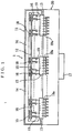
- Fig. 1 shows a conventionally used thick film-type thermal printhead 1.
- a thermal printhead according to the present invention has a structure similar to that shown in Fig. 1 except for its characteristic portions.
- the thermal printhead 1 shown in Fig. 1 includes a head substrate 11 formed of alumina ceramic and an additional substrate 20 formed of glass-fiber-reinforced epoxy resin.
- the head substrate 11 is provided with a linear heating resistor 12, a plurality of drive ICs 13, a common electrode 14 and a plurality of individual electrodes 15.
- the heating resistor 12 extends longitudinally of the head substrate.
- the drive ICs 13 are arranged in a row extending in the longitudinal direction of the head substrate.
- the common electrode 14 is integrally formed with a plurality of comb-teeth like projections 16 extending parallel to each other. Each projection 16 has a free end electrically connected to the heating resistor 12.
- Each individual electrode 15 is linear and has two free ends. As shown in Fig. 1, the individual electrodes 15 and the plurality of projections 16 are alternately disposed. One free end of each individual electrode 15 is positioned between two adjacent projections 16 of the common electrode 14 to be electrically connected to the heating resistor 12, whereas the other free end is connected, via a conductive wire 19, to an output pad (not shown) of a relevant drive IC 13.
- the heating resistor 12 includes a plurality of regions 18 each defined between two adjacent projections 16.
- These regions function as heating dots under the control of the drive ICs 13. Specifically, a current is supplied to the region 18 selected by the drive ICs 13 via the adjacent projection 16 and the individual electrode 15. As a result, the selected region is heated up to function as a heating dot.
- the additional substrate 20 is formed with a wiring pattern (partially shown) which is connected to input pads (not shown) of the drive ICs 13 via a plurality of conductive wires 19a.
- the additional substrate 20 is further provided with a connector 17 connected to the wiring pattern.
- the connector 17 is also connected to a cable (not shown) for transmitting signals supplied from outside. With the above arrangement, the external signals are transmitted via the wiring pattern to the drive ICs 13. The drive ICs 13 will operate based on the thus transmitted signals.
- Each of the drive ICs 13 incorporates a shift register which has a predetermined number of bits corresponding to the number of the output pads of the drive IC 13.
- the drive ICs 13 have their data-out terminals connected in cascade to their data-in terminals, so that the shift registers in the respective drive ICs 13 are connected to each other.
- the thermal printhead having the above structure operates as follows.
- printing data for the line need be input to the drive ICs 13 in advance.
- the printing data for the line are serially fed to the leftmost drive IC 13 shown in Fig. 1 via the data-in terminal.
- the printing data are successively fed to the shift registers of the respective drive ICs 13 connected in cascade to each other, and retained in them.
- the output pads of the drive ICs 13 are selectively actuated in synchronism with a strobe signal fed to each drive IC 13.
- the heating dots 18 are selectively heated up for performing a predetermined printing operation.
- the thermal printhead 1 having the above arrangement has the following problems. Since the printing data for one line are serially fed to the drive ICs 13, the printing operation for the line cannot be started until the input of the serial data is completed. This means that, in the above thermal printhead, it is impossible to improve the printing speed beyond a certain limit due to the serial data input. Further, when all the heating dots 18 are actuated simultaneously, an increased amount of current will pass through the common electrode 14. Consequently, the voltage drop along the common electrode 14 is intensified, which leads to uneven printing results.
- the above method suffers the following problem.
- a special wiring pattern designed for that particular purpose is needed. Therefore, it is necessary to prepare different kinds of wiring patterns, such as a wiring pattern suitable for the use of two-grouped printing data or a wiring pattern suitable for the use of three-grouped printing data, depending on the characteristics of a device in which the thermal printhead 1 is incorporated or on the need of a user.
- To individually manufacture such thermal printheads having different kinds of wiring patterns requires additional time and trouble, thereby leading to an increase in cost.
- a wiring pattern for supplying strobe signals needs to be additionally designed in accordance with the particular divisional manner.
- the design of the various wiring patterns mentioned above may need to be altered after they are produced. For instance, a user may wish to use a wiring pattern designed for three-grouped printing data in place of the originally used wiring pattern designed for two-grouped printing data. Conventionally, in such a situation, a thermal printhead incorporating a wiring pattern designed for three-grouped printing data may need to be purchased additionally, which is very inconvenient.
- a thermal printhead comprising:
- a selected one of the severable site of said each main conductor wiring and the severable site of the auxiliary conductor wiring accompanying said each main conductor wiring may be severed.
- Each of the severable sites may be formed with a marking.
- the thermal printhead may further comprise a plurality of recovery wiring portions arranged in parallel to the severable sites, respectively.
- Each recovery wiring portion may include a pair of pads spaced from each other.
- a thermal printhead according to the present invention has a structure substantially the same as that of the conventional thermal printhead shown in Fig. 1. Therefore, the thermal printhead according to the present invention will also be described with reference to Fig. 1 (and other figures).
- the thermal printhead 1 includes a head substrate 11 formed of e.g., alumina ceramic, and an additional substrate 20 formed of e.g., glass-fiber-reinforced epoxy resin.
- the head substrate 11 is provided with a linear heating resistor 12, a plurality of drive ICs 13, a common electrode 14 and a plurality of individual electrodes 15.
- the heating resistor 12 extends longitudinally of the head substrate.
- the drive ICs 13 are linearly disposed in the longitudinal direction of the head substrate.
- the common electrode 14 is integrally formed with a plurality of comb-teeth like projections 16 extending parallel to each other. Each projection 16 has a free end electrically connected to the heating resistor 12.
- Each individual electrode 15 has an elongated configuration and has two free ends. As shown in Fig. 1, the individual electrodes 15 and the plurality of projections 16 are alternately disposed. One free end of each individual electrode 15 is positioned between two adjacent projections 16 of the common electrode 14 to be electrically connected to the heating resistor 12. On the other hand, the other free end of the individual electrode 15 is connected, via a conductive wire 19 such as a gold wire, to an output pad (not shown) of a relevant drive IC 13. Each of the drive ICs 13 is provided with power and signal pads (not shown). Further each drive IC 13 incorporates a shift register. The shift register has a predetermined number of bits corresponding in number to the output pads of the drive IC 13.
- the heating resistor 12 includes a plurality of regions 18 (See Fig. 1) each of which is defined by adjacent projections 16.
- the respective regions operate as heating dots under control of the drive ICs 13. More specifically, a current is supplied to the region 18 selected by the drive ICs 13, via the adjacent projection 16 and the individual electrode 15. As a result, the particular region is heated up to function as a heating dot.
- the additional substrate 20 carries a connector 17. This connector 17 is arranged to be connected to a cable (not shown) which is used for transmitting signals supplied from outside.
- the additional substrate 20 is further formed with a wiring pattern which is connected to e.g., the signal pads of the drive ICs 13 via wires 19a.
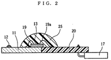
- the drive IC 13, the bonding wires 19, 19a are covered with a protective coating 25 formed of e.g., a hard coating material.
- the most significant feature of the present invention is the wiring pattern formed on the head substrate 20. This wiring pattern will be described below with reference to Fig. 3.
- the illustrated wiring pattern is designed so that printing data for one line supplied via the connector 17 are transmitted to the drive ICs 13 in a manner which permits the printing data to be divided into a maximum of four groups.
- the fourteen drive ICs 13 are divided into four groups.
- the first group includes four drive ICs (DrIC1-4), the second group three drive ICs (DrIC5-7), the third group four drive ICs (DrIC8-11), and the fourth group three drive ICs (DrIC12-14).
- the drive ICs are electrically connected to each other.
- the illustrated wiring pattern includes four main conductor wirings 31-34 and three auxiliary conductor wirings 41-43. One ends of the respective main conductor wirings 31-34 are connected to the connector 17. The other ends of the main conductor wirings 31-34 are connected, respectively, to the data-in pad (DI) of the drive IC (DrIC1), the data-in pad (DI) of the drive IC (DrIC5), the data-in pad (DI) of the drive IC (DrIC8), and the data-in pad (DI) of the drive IC (DrIC12).
- DI data-in pad
- the three auxiliary conductor wirings 41-43 are arranged to connect, respectively, the data-out pad (DO) of the drive IC (DrIC4) to the data-in pad (DI) of the drive IC (DrIC5), the data-out pad (DO) of the drive IC (DrIC7) to the data-in pad (DI) of the drive IC (DrIC8), and the data-out pad (DO) of the drive IC (DrIC11) to the data-in pad (DI) of the drive IC (DrIC12).
- the main conductor wirings 32-34 are provided with severable sites d-f respectively for severing electrical conduction of the main conductor wirings.
- the severable sites may be provided with predetermined markings for facilitating visual recognition.
- the auxiliary conductor wirings 41-43 are provided with severable sites a-c respectively for severing electrical conduction of the auxiliary conductor wirings.
- the severable sites may also be provided with predetermined markings.
- the main conductor wirings 32-34 are provided with recovery wiring portions 32a-34a, respectively, each of which extends so as to bridge a corresponding one of the severable sites d-f.
- Each of the recovery wiring portions includes two spaced pads and conductor wirings for connecting the respective pads to the main conductor wiring.
- the auxiliary conductor wirings 41-43 are provided with recovery wiring portions 41a-43a, respectively, each of which extends to bridge a corresponding one of the severable sites a-c.
- Each of the recovery wiring portions includes two spaced pads and conductor wirings for connecting the respective pads to the auxiliary conductor wiring.
- Each severable site may be bypassed by connecting the two spaced pads of the recovery wiring portion by soldering or wire-bonding.
- the wiring pattern thus formed may be utilized as follows. It should be noted that, in the description given below, all the severable portions a-f are depicted as being connected in the initial state.
- the one-line printing data divided into four groups are to be supplied to the drive ICs.
- the severable portions a, b and c shown in Fig. 3 will be severed by etching or NC machining for example.
- a piece of printing data supplied through the main conductor wiring 31 is transmitted from the leftmost drive IC (DrIC1) to the rightmost drive IC (DrIC4) of the first group.
- a piece of printing data supplied through the main conductor wiring 32 is transmitted from the leftmost drive IC (DrIC5) to the rightmost drive IC (DrIC7) of the second group
- a piece of printing data supplied through the main conductor wiring 33 is transmitted from the leftmost drive IC (DrIC8) to the rightmost drive IC (DrIC11) of the third group
- a piece of printing data supplied through the main conductor wiring 34 is transmitted from the leftmost drive IC (DrIC12) to the rightmost drive IC (DrIC14) of the fourth group.
- the one-line printing data are to be divided into two groups for supply to the drive ICs.
- the severable portions b, d and f are severed, as may easily be understood.
- the whole one-line printing data are serially transmitted in one gruop, the severable portions d, e and f are severed.
- the wiring pattern can be altered into the two division form in the following manner. First, the severable portions d and f are severed. Then, the recovery wiring portions 41a, 43a are electrically connected. As a result, the wiring pattern is modified so that the one-line printing data divided into two groups will be transmitted to the drive ICs.
- a single wiring pattern can be modified to a selected one of the one-division, two-division and four-division patterns, as required, in the above-described manner.
- main conductor wiring and the auxiliary conductor wiring are to be severed by useing a NC machining technique, it suffices to prepare a new program for controlling the movement of the processing head of the device performing the NC machining. This requires less time and trouble than the additional designing of a plurality of wiring patterns.
- the drive ICs 13 are divided into four groups. However, it is obvious that the drive ICs 13 may be divided into another number of groups.
- the main conductor wirings and the auxiliary conductor wirings are described as being initially connected at the severable portions.
- all the severable portions may be severed in the initial state. Even in this case, it is possible to achieve a desired number of division by connecting the spaced pads of the recovery wiring portions. It may also be possible to have only one selected severable portion severed in the initial state.
- the wiring pattern for transmitting printing data is described.
- the present invention may be applied to a wiring pattern for transmitting clock signals, strobe signals, or strobe clock signals.
- the wiring pattern and the drive ICs are mounted on separate substrates 10 and 11, respectively.
- the wiring pattern and the drive ICs may be mounted on a common substrate.
- the present invention is applied to a thick film-type thermal printhead in the above embodiment.
- the present invention may also be applied to a thin film-type thermal printhead.
- the thermal printhead according to the present invention may advantageously be used based on one-line printing data or the like which may be divided into plural pieces.
Landscapes
- Electronic Switches (AREA)
Abstract
Description
- The present invention relates to a thermal printhead for forming images on thermosensitive paper or on recording paper via a thermal-transfer ink ribbon.
- As is well known, thermal printheads are used for forming intended images by selectively providing thermal energy to thermosensitive paper or a thermal-transfer ink ribbon. Generally, thermal printheads are divided mainly into thin film-type thermal printheads and thick film-type thermal printheads depending on methods of forming their heating resistors. As an example, a typical thick film-type thermal printhead will be described below.
- Fig. 1 shows a conventionally used thick film-type thermal printhead 1. As will be described later, a thermal printhead according to the present invention has a structure similar to that shown in Fig. 1 except for its characteristic portions.
- The thermal printhead 1 shown in Fig. 1 includes a
head substrate 11 formed of alumina ceramic and anadditional substrate 20 formed of glass-fiber-reinforced epoxy resin. Thehead substrate 11 is provided with alinear heating resistor 12, a plurality ofdrive ICs 13, acommon electrode 14 and a plurality ofindividual electrodes 15. Theheating resistor 12 extends longitudinally of the head substrate. Thedrive ICs 13 are arranged in a row extending in the longitudinal direction of the head substrate. - The
common electrode 14 is integrally formed with a plurality of comb-teeth likeprojections 16 extending parallel to each other. Eachprojection 16 has a free end electrically connected to theheating resistor 12. Eachindividual electrode 15 is linear and has two free ends. As shown in Fig. 1, theindividual electrodes 15 and the plurality ofprojections 16 are alternately disposed. One free end of eachindividual electrode 15 is positioned between twoadjacent projections 16 of thecommon electrode 14 to be electrically connected to theheating resistor 12, whereas the other free end is connected, via aconductive wire 19, to an output pad (not shown) of arelevant drive IC 13. With such an arrangement, theheating resistor 12 includes a plurality ofregions 18 each defined between twoadjacent projections 16. These regions function as heating dots under the control of thedrive ICs 13. Specifically, a current is supplied to theregion 18 selected by thedrive ICs 13 via theadjacent projection 16 and theindividual electrode 15. As a result, the selected region is heated up to function as a heating dot. - The
additional substrate 20 is formed with a wiring pattern (partially shown) which is connected to input pads (not shown) of thedrive ICs 13 via a plurality ofconductive wires 19a. Theadditional substrate 20 is further provided with aconnector 17 connected to the wiring pattern. Theconnector 17 is also connected to a cable (not shown) for transmitting signals supplied from outside. With the above arrangement, the external signals are transmitted via the wiring pattern to thedrive ICs 13. Thedrive ICs 13 will operate based on the thus transmitted signals. - Each of the
drive ICs 13 incorporates a shift register which has a predetermined number of bits corresponding to the number of the output pads of thedrive IC 13. Thedrive ICs 13 have their data-out terminals connected in cascade to their data-in terminals, so that the shift registers in therespective drive ICs 13 are connected to each other. - The thermal printhead having the above structure operates as follows. In order to perform printing for one line, printing data for the line need be input to the
drive ICs 13 in advance. To this end, the printing data for the line are serially fed to theleftmost drive IC 13 shown in Fig. 1 via the data-in terminal. Then, the printing data are successively fed to the shift registers of therespective drive ICs 13 connected in cascade to each other, and retained in them. In accordance with the retained printing data, the output pads of thedrive ICs 13 are selectively actuated in synchronism with a strobe signal fed to eachdrive IC 13. As a result, theheating dots 18 are selectively heated up for performing a predetermined printing operation. - Unfavorably, the thermal printhead 1 having the above arrangement has the following problems. Since the printing data for one line are serially fed to the
drive ICs 13, the printing operation for the line cannot be started until the input of the serial data is completed. This means that, in the above thermal printhead, it is impossible to improve the printing speed beyond a certain limit due to the serial data input. Further, when all theheating dots 18 are actuated simultaneously, an increased amount of current will pass through thecommon electrode 14. Consequently, the voltage drop along thecommon electrode 14 is intensified, which leads to uneven printing results. - To deal with the above problems, the following measures have conventionally been taken. To begin with, printing data for one line are divided into a predetermined number of pieces, while the
drive ICs 13 are also divided into the same number of groups. Then, each piece of the divided printing data is simultaneously fed to a corresponding one of the groups of thedrive ICs 13. Compared with the serial input described above, this method is advantageous in that the printing data can be fed to thedrive ICs 13 more quickly, so that the printing speed is improved. In addition, by staggering the timing of driving the respective groups ofdrive ICs 13, the current flowing through thecommon electrode 14 will be decreased, thereby reducing the voltage drop along thecommon electrode 14. - However, the above method suffers the following problem. To feed the divided data to the respective groups of
drive ICs 13, a special wiring pattern designed for that particular purpose is needed. Therefore, it is necessary to prepare different kinds of wiring patterns, such as a wiring pattern suitable for the use of two-grouped printing data or a wiring pattern suitable for the use of three-grouped printing data, depending on the characteristics of a device in which the thermal printhead 1 is incorporated or on the need of a user. To individually manufacture such thermal printheads having different kinds of wiring patterns requires additional time and trouble, thereby leading to an increase in cost. Further, in order to actuate thedrive ICs 13 group by group with time difference, a wiring pattern for supplying strobe signals needs to be additionally designed in accordance with the particular divisional manner. - Moreover, the design of the various wiring patterns mentioned above may need to be altered after they are produced. For instance, a user may wish to use a wiring pattern designed for three-grouped printing data in place of the originally used wiring pattern designed for two-grouped printing data. Conventionally, in such a situation, a thermal printhead incorporating a wiring pattern designed for three-grouped printing data may need to be purchased additionally, which is very inconvenient.
- Therefore, it is an object of the present invention to provide a thermal printhead which is capable of solving the above problems.
- In accordance with the present invention, there is provided a thermal printhead comprising:
- drive ICs divided into a plurality of groups;
- a plurality of main conductor wirings for transmitting signals to the respective groups of the drive ICs; and
- a plurality of auxiliary conductor wirings arranged to
accompany the main conductor wirings, respectively, for
connecting the drive ICs in adjacent groups;
wherein each main conductor wiring and each auxiliary conductor wiring include a severable site for severing electrical conduction of said each main conductor wiring and said each auxiliary conductor wiring. -
- In the thermal printhead having the above arrangement, a selected one of the severable site of said each main conductor wiring and the severable site of the auxiliary conductor wiring accompanying said each main conductor wiring may be severed.
- Furhter, all the severable sites of the main conductor wirings may be severed. Still further, all the severable sites of the auxiliary conductor wirings may be severed.
- Each of the severable sites may be formed with a marking.
- Preferably, the thermal printhead may further comprise a plurality of recovery wiring portions arranged in parallel to the severable sites, respectively. Each recovery wiring portion may include a pair of pads spaced from each other.
- Various features and advantages of the present invention will become clearer from the description given below with reference to the accompanying drawings.
-
- Fig. 1 is a plan view showing arrangements of a thermal printhead which are common to the prior art and the present invention.
- Fig. 2 is a sectional view showing the same thermal printhead.
- Fig. 3 is a schematic view showing a wiring pattern for the printing data according to the present invention.
-
- As previously described, a thermal printhead according to the present invention has a structure substantially the same as that of the conventional thermal printhead shown in Fig. 1. Therefore, the thermal printhead according to the present invention will also be described with reference to Fig. 1 (and other figures).
- Specifically, the thermal printhead 1 according to the present invention includes a
head substrate 11 formed of e.g., alumina ceramic, and anadditional substrate 20 formed of e.g., glass-fiber-reinforced epoxy resin. Thehead substrate 11 is provided with alinear heating resistor 12, a plurality ofdrive ICs 13, acommon electrode 14 and a plurality ofindividual electrodes 15. Theheating resistor 12 extends longitudinally of the head substrate. Thedrive ICs 13 are linearly disposed in the longitudinal direction of the head substrate. - The
common electrode 14 is integrally formed with a plurality of comb-teeth likeprojections 16 extending parallel to each other. Eachprojection 16 has a free end electrically connected to theheating resistor 12. Eachindividual electrode 15 has an elongated configuration and has two free ends. As shown in Fig. 1, theindividual electrodes 15 and the plurality ofprojections 16 are alternately disposed. One free end of eachindividual electrode 15 is positioned between twoadjacent projections 16 of thecommon electrode 14 to be electrically connected to theheating resistor 12. On the other hand, the other free end of theindividual electrode 15 is connected, via aconductive wire 19 such as a gold wire, to an output pad (not shown) of arelevant drive IC 13. Each of thedrive ICs 13 is provided with power and signal pads (not shown). Further each driveIC 13 incorporates a shift register. The shift register has a predetermined number of bits corresponding in number to the output pads of thedrive IC 13. - With the above arrangement, the
heating resistor 12 includes a plurality of regions 18 (See Fig. 1) each of which is defined byadjacent projections 16. The respective regions operate as heating dots under control of thedrive ICs 13. More specifically, a current is supplied to theregion 18 selected by thedrive ICs 13, via theadjacent projection 16 and theindividual electrode 15. As a result, the particular region is heated up to function as a heating dot. - The
additional substrate 20 carries aconnector 17. Thisconnector 17 is arranged to be connected to a cable (not shown) which is used for transmitting signals supplied from outside. Theadditional substrate 20 is further formed with a wiring pattern which is connected to e.g., the signal pads of thedrive ICs 13 viawires 19a. - As shown in Fig. 2, the
drive IC 13, thebonding wires protective coating 25 formed of e.g., a hard coating material. - The most significant feature of the present invention is the wiring pattern formed on the
head substrate 20. This wiring pattern will be described below with reference to Fig. 3. - The illustrated wiring pattern is designed so that printing data for one line supplied via the
connector 17 are transmitted to thedrive ICs 13 in a manner which permits the printing data to be divided into a maximum of four groups. Specifically, the fourteendrive ICs 13 are divided into four groups. The first group includes four drive ICs (DrIC1-4), the second group three drive ICs (DrIC5-7), the third group four drive ICs (DrIC8-11), and the fourth group three drive ICs (DrIC12-14). In each group, the drive ICs are electrically connected to each other. - The illustrated wiring pattern includes four main conductor wirings 31-34 and three auxiliary conductor wirings 41-43. One ends of the respective main conductor wirings 31-34 are connected to the
connector 17. The other ends of the main conductor wirings 31-34 are connected, respectively, to the data-in pad (DI) of the drive IC (DrIC1), the data-in pad (DI) of the drive IC (DrIC5), the data-in pad (DI) of the drive IC (DrIC8), and the data-in pad (DI) of the drive IC (DrIC12). The three auxiliary conductor wirings 41-43 are arranged to connect, respectively, the data-out pad (DO) of the drive IC (DrIC4) to the data-in pad (DI) of the drive IC (DrIC5), the data-out pad (DO) of the drive IC (DrIC7) to the data-in pad (DI) of the drive IC (DrIC8), and the data-out pad (DO) of the drive IC (DrIC11) to the data-in pad (DI) of the drive IC (DrIC12). - The main conductor wirings 32-34 are provided with severable sites d-f respectively for severing electrical conduction of the main conductor wirings. The severable sites may be provided with predetermined markings for facilitating visual recognition. Similarly, the auxiliary conductor wirings 41-43 are provided with severable sites a-c respectively for severing electrical conduction of the auxiliary conductor wirings. The severable sites may also be provided with predetermined markings.
- Further, the main conductor wirings 32-34 are provided with
recovery wiring portions 32a-34a, respectively, each of which extends so as to bridge a corresponding one of the severable sites d-f. Each of the recovery wiring portions includes two spaced pads and conductor wirings for connecting the respective pads to the main conductor wiring. Similarly, the auxiliary conductor wirings 41-43 are provided withrecovery wiring portions 41a-43a, respectively, each of which extends to bridge a corresponding one of the severable sites a-c. Each of the recovery wiring portions includes two spaced pads and conductor wirings for connecting the respective pads to the auxiliary conductor wiring. Each severable site may be bypassed by connecting the two spaced pads of the recovery wiring portion by soldering or wire-bonding. - The wiring pattern thus formed may be utilized as follows. It should be noted that, in the description given below, all the severable portions a-f are depicted as being connected in the initial state.
- It is now supposed that the one-line printing data divided into four groups are to be supplied to the drive ICs. In this case, the severable portions a, b and c shown in Fig. 3 will be severed by etching or NC machining for example. In this manner, a piece of printing data supplied through the
main conductor wiring 31 is transmitted from the leftmost drive IC (DrIC1) to the rightmost drive IC (DrIC4) of the first group. Similarly, a piece of printing data supplied through themain conductor wiring 32 is transmitted from the leftmost drive IC (DrIC5) to the rightmost drive IC (DrIC7) of the second group, a piece of printing data supplied through themain conductor wiring 33 is transmitted from the leftmost drive IC (DrIC8) to the rightmost drive IC (DrIC11) of the third group, and a piece of printing data supplied through themain conductor wiring 34 is transmitted from the leftmost drive IC (DrIC12) to the rightmost drive IC (DrIC14) of the fourth group. - Now, it is supposed that the one-line printing data are to be divided into two groups for supply to the drive ICs. In this case, the severable portions b, d and f are severed, as may easily be understood. Alternatively, when the whole one-line printing data are serially transmitted in one gruop, the severable portions d, e and f are severed.
- Once the severable portions a, b and c have been severed for enabling four-group transmission of the printing data, the wiring pattern can be altered into the two division form in the following manner. First, the severable portions d and f are severed. Then, the
recovery wiring portions - In the thermal printhead 1 of the present invention, as is clear from the above, a single wiring pattern can be modified to a selected one of the one-division, two-division and four-division patterns, as required, in the above-described manner. Thus, it is possible to provide various kinds of divisional patterns without individually preparing the wiring patterns corresponding to the respective divisions. Therefore, in the thermal printhead 1 formed with the wiring pattern described above, by severing the main conductor wiring or the auxiliary conductor wiring, the drive ICs may be divided into a desired number of groups in accordance with the order from a user for example. Thus, the time and trouble taken for designing can be reduced.
- Further, when the main conductor wiring and the auxiliary conductor wiring are to be severed by useing a NC machining technique, it suffices to prepare a new program for controlling the movement of the processing head of the device performing the NC machining. This requires less time and trouble than the additional designing of a plurality of wiring patterns.
- Further, as described above, it is possible to reconnect the once severed auxiliary conductor wirings 41, 42, 43 by connecting the
recovery wiring portions 41a, 42b and 43c. This means that the divisional number once determined can be altered. It is clear that the similar operation can be performed with respect to the main conductor wirings 32-34 provided with therecovery wiring portions 32a-34a. - In the above embodiment, the
drive ICs 13 are divided into four groups. However, it is obvious that thedrive ICs 13 may be divided into another number of groups. - Further, in the above embodiment, the main conductor wirings and the auxiliary conductor wirings are described as being initially connected at the severable portions. Alternatively, all the severable portions may be severed in the initial state. Even in this case, it is possible to achieve a desired number of division by connecting the spaced pads of the recovery wiring portions. It may also be possible to have only one selected severable portion severed in the initial state.
- In the above embodiment, the wiring pattern for transmitting printing data is described. The present invention, however, may be applied to a wiring pattern for transmitting clock signals, strobe signals, or strobe clock signals.
- Further, in the above embodiment, the wiring pattern and the drive ICs are mounted on
separate substrates 10 and 11, respectively. However, the wiring pattern and the drive ICs may be mounted on a common substrate. - The present invention is applied to a thick film-type thermal printhead in the above embodiment. However, the present invention may also be applied to a thin film-type thermal printhead.
- As described hereinbefore, the thermal printhead according to the present invention may advantageously be used based on one-line printing data or the like which may be divided into plural pieces.
Claims (7)
- A thermal printhead comprising:drive ICs divided into a plurality of groups;a plurality of main conductor wirings for transmitting signals to the respective groups of the drive ICs; anda plurality of auxiliary conductor wirings arranged to accompany the main conductor wirings, respectively, for connecting the drive ICs in adjacent groups;
wherein each main conductor wiring and each auxiliary conductor wiring include a severable site for severing electrical conduction of said each main conductor wiring and said each auxiliary conductor wiring. - The thermal printhead according to claim 1, wherein a selected one of the severable site of said each main conductor wiring and the severable site of the auxiliary conductor wiring accompanying said each main conductor wiring is severed.
- The thermal printhead according to claim 1, wherein all the severable sites of the main conductor wirings are severed.
- The thermal printhead according to claim 1, wherein all the severable sites of the auxiliary conductor wirings are severed.
- The thermal printhead according to claim 1, wherein each of the severable sites is formed with a marking.
- The thermal printhead according to claim 1, further comprising a plurality of recovery wiring portions arranged in parallel to the severable sites, respectively.
- The thermal printhead according to claim 6, wherein each recovery wiring portion includes a pair of pads spaced from each other.
Applications Claiming Priority (3)
| Application Number | Priority Date | Filing Date | Title |
|---|---|---|---|
| JP8060297 | 1997-03-31 | ||
| JP8060297 | 1997-03-31 | ||
| PCT/JP1998/001496 WO1998043819A1 (en) | 1997-03-31 | 1998-03-31 | Thermal printing head |
Publications (3)
| Publication Number | Publication Date |
|---|---|
| EP1013454A1 true EP1013454A1 (en) | 2000-06-28 |
| EP1013454A4 EP1013454A4 (en) | 2001-01-17 |
| EP1013454B1 EP1013454B1 (en) | 2006-12-13 |
Family
ID=13722889
Family Applications (1)
| Application Number | Title | Priority Date | Filing Date |
|---|---|---|---|
| EP98911150A Expired - Lifetime EP1013454B1 (en) | 1997-03-31 | 1998-03-31 | Thermal printing head |
Country Status (7)
| Country | Link |
|---|---|
| US (1) | US6222574B1 (en) |
| EP (1) | EP1013454B1 (en) |
| JP (1) | JP3993247B2 (en) |
| KR (1) | KR100337626B1 (en) |
| CN (1) | CN1093471C (en) |
| DE (1) | DE69836639T2 (en) |
| WO (1) | WO1998043819A1 (en) |
Families Citing this family (1)
| Publication number | Priority date | Publication date | Assignee | Title |
|---|---|---|---|---|
| CN100496980C (en) * | 2004-06-02 | 2009-06-10 | 佳能株式会社 | Head substrate, recording head, head cartridge, and recorder |
Family Cites Families (1)
| Publication number | Priority date | Publication date | Assignee | Title |
|---|---|---|---|---|
| JPS61239957A (en) | 1985-04-16 | 1986-10-25 | Nec Corp | Preparation of substrate for thermal head |
-
1998
- 1998-03-31 EP EP98911150A patent/EP1013454B1/en not_active Expired - Lifetime
- 1998-03-31 WO PCT/JP1998/001496 patent/WO1998043819A1/en not_active Ceased
- 1998-03-31 DE DE69836639T patent/DE69836639T2/en not_active Expired - Fee Related
- 1998-03-31 US US09/381,691 patent/US6222574B1/en not_active Expired - Lifetime
- 1998-03-31 CN CN98803854A patent/CN1093471C/en not_active Expired - Fee Related
- 1998-03-31 KR KR1019997008467A patent/KR100337626B1/en not_active Expired - Fee Related
- 1998-03-31 JP JP54146798A patent/JP3993247B2/en not_active Expired - Lifetime
Non-Patent Citations (2)
| Title |
|---|
| No further relevant documents disclosed * |
| See also references of WO9843819A1 * |
Also Published As
| Publication number | Publication date |
|---|---|
| JP3993247B2 (en) | 2007-10-17 |
| CN1251552A (en) | 2000-04-26 |
| KR100337626B1 (en) | 2002-05-24 |
| CN1093471C (en) | 2002-10-30 |
| EP1013454B1 (en) | 2006-12-13 |
| KR20000076365A (en) | 2000-12-26 |
| EP1013454A4 (en) | 2001-01-17 |
| DE69836639T2 (en) | 2007-09-27 |
| DE69836639D1 (en) | 2007-01-25 |
| WO1998043819A1 (en) | 1998-10-08 |
| US6222574B1 (en) | 2001-04-24 |
Similar Documents
| Publication | Publication Date | Title |
|---|---|---|
| KR930005792A (en) | Printheads and Printers with the Same | |
| US6222574B1 (en) | Thermal printing head | |
| US5729275A (en) | Thermal printhead, drive IC for the same and method for controlling the thermal printhead | |
| EP0466968B1 (en) | Thermal recording system and thermal recording head | |
| US6611280B1 (en) | Flexible cable, flexible cable mount method, semiconductor device with flexible cable, led array head with flexible cable, image forming apparatus with such led array head | |
| US4636813A (en) | Thermal print head | |
| CN111823723B (en) | Thermal print head, and driving IC and wiring pattern used for the same | |
| EP0729840B1 (en) | Ic for driving printer and print head | |
| EP0491388B1 (en) | Thermal printing head | |
| JPWO1998043819A1 (en) | thermal printhead | |
| EP0186059B1 (en) | Thermal print head | |
| JP2976087B2 (en) | Thermal print head and method of manufacturing the same | |
| US5166700A (en) | Thermal print head | |
| JPWO1996011109A1 (en) | Printer driver IC and print head using same | |
| JPH0563022A (en) | Head drive IC and head substrate | |
| EP0581330B1 (en) | Drive IC for printing head | |
| KR20010041108A (en) | Driver ic chip and print head | |
| JP2633701B2 (en) | Thermal head | |
| JP2881631B2 (en) | Drive IC for thermal print head, thermal print head using the same, and method of controlling this thermal print head | |
| JPH0584946A (en) | Thermal printing head substrate and production thereof | |
| JP3300868B2 (en) | Drive IC for print head and print head using the same | |
| JP2734051B2 (en) | Thermal recording head | |
| JP2580454Y2 (en) | Thermal head | |
| JPS60230873A (en) | Thermal printer | |
| JP3180290B2 (en) | Thermal head |
Legal Events
| Date | Code | Title | Description |
|---|---|---|---|
| PUAI | Public reference made under article 153(3) epc to a published international application that has entered the european phase |
Free format text: ORIGINAL CODE: 0009012 |
|
| 17P | Request for examination filed |
Effective date: 19990923 |
|
| AK | Designated contracting states |
Kind code of ref document: A1 Designated state(s): DE FR GB IT |
|
| A4 | Supplementary search report drawn up and despatched |
Effective date: 20001206 |
|
| AK | Designated contracting states |
Kind code of ref document: A4 Designated state(s): DE FR GB IT |
|
| RIC1 | Information provided on ipc code assigned before grant |
Free format text: 7B 41J 2/335 A, 7B 41J 2/345 B, 7B 41J 2/355 B |
|
| GRAP | Despatch of communication of intention to grant a patent |
Free format text: ORIGINAL CODE: EPIDOSNIGR1 |
|
| GRAS | Grant fee paid |
Free format text: ORIGINAL CODE: EPIDOSNIGR3 |
|
| GRAA | (expected) grant |
Free format text: ORIGINAL CODE: 0009210 |
|
| AK | Designated contracting states |
Kind code of ref document: B1 Designated state(s): DE FR GB IT |
|
| REG | Reference to a national code |
Ref country code: GB Ref legal event code: FG4D |
|
| REF | Corresponds to: |
Ref document number: 69836639 Country of ref document: DE Date of ref document: 20070125 Kind code of ref document: P |
|
| ET | Fr: translation filed | ||
| PLBE | No opposition filed within time limit |
Free format text: ORIGINAL CODE: 0009261 |
|
| STAA | Information on the status of an ep patent application or granted ep patent |
Free format text: STATUS: NO OPPOSITION FILED WITHIN TIME LIMIT |
|
| 26N | No opposition filed |
Effective date: 20070914 |
|
| PGFP | Annual fee paid to national office [announced via postgrant information from national office to epo] |
Ref country code: GB Payment date: 20090325 Year of fee payment: 12 |
|
| PGFP | Annual fee paid to national office [announced via postgrant information from national office to epo] |
Ref country code: IT Payment date: 20090318 Year of fee payment: 12 Ref country code: DE Payment date: 20090327 Year of fee payment: 12 |
|
| PGFP | Annual fee paid to national office [announced via postgrant information from national office to epo] |
Ref country code: FR Payment date: 20090316 Year of fee payment: 12 |
|
| GBPC | Gb: european patent ceased through non-payment of renewal fee |
Effective date: 20100331 |
|
| REG | Reference to a national code |
Ref country code: FR Ref legal event code: ST Effective date: 20101130 |
|
| PG25 | Lapsed in a contracting state [announced via postgrant information from national office to epo] |
Ref country code: FR Free format text: LAPSE BECAUSE OF NON-PAYMENT OF DUE FEES Effective date: 20100331 |
|
| PG25 | Lapsed in a contracting state [announced via postgrant information from national office to epo] |
Ref country code: DE Free format text: LAPSE BECAUSE OF NON-PAYMENT OF DUE FEES Effective date: 20101001 |
|
| PG25 | Lapsed in a contracting state [announced via postgrant information from national office to epo] |
Ref country code: GB Free format text: LAPSE BECAUSE OF NON-PAYMENT OF DUE FEES Effective date: 20100331 Ref country code: IT Free format text: LAPSE BECAUSE OF NON-PAYMENT OF DUE FEES Effective date: 20100331 |