EP1013430B1 - High density electrical interconnect for a continuous ink jet printhead - Google Patents
High density electrical interconnect for a continuous ink jet printhead Download PDFInfo
- Publication number
- EP1013430B1 EP1013430B1 EP19990309493 EP99309493A EP1013430B1 EP 1013430 B1 EP1013430 B1 EP 1013430B1 EP 19990309493 EP19990309493 EP 19990309493 EP 99309493 A EP99309493 A EP 99309493A EP 1013430 B1 EP1013430 B1 EP 1013430B1
- Authority
- EP
- European Patent Office
- Prior art keywords
- array
- contact pads
- charge plate
- charge
- leads
- Prior art date
- Legal status (The legal status is an assumption and is not a legal conclusion. Google has not performed a legal analysis and makes no representation as to the accuracy of the status listed.)
- Expired - Lifetime
Links
- 238000000034 method Methods 0.000 description 20
- 230000013011 mating Effects 0.000 description 12
- 229920001971 elastomer Polymers 0.000 description 4
- 239000000806 elastomer Substances 0.000 description 4
- 238000003491 array Methods 0.000 description 3
- 239000004593 Epoxy Substances 0.000 description 2
- 239000000853 adhesive Substances 0.000 description 2
- 230000001070 adhesive effect Effects 0.000 description 2
- 239000000919 ceramic Substances 0.000 description 2
- 238000005323 electroforming Methods 0.000 description 2
- 238000005516 engineering process Methods 0.000 description 2
- 238000004519 manufacturing process Methods 0.000 description 2
- 238000007639 printing Methods 0.000 description 2
- 230000009467 reduction Effects 0.000 description 2
- 238000005476 soldering Methods 0.000 description 2
- 239000003351 stiffener Substances 0.000 description 2
- 230000006835 compression Effects 0.000 description 1
- 238000007906 compression Methods 0.000 description 1
- 239000012141 concentrate Substances 0.000 description 1
- 239000011231 conductive filler Substances 0.000 description 1
- 238000007641 inkjet printing Methods 0.000 description 1
- 238000002955 isolation Methods 0.000 description 1
- 238000010030 laminating Methods 0.000 description 1
- 239000000463 material Substances 0.000 description 1
- 239000002184 metal Substances 0.000 description 1
- 238000000206 photolithography Methods 0.000 description 1
- 238000007650 screen-printing Methods 0.000 description 1
- 229910000679 solder Inorganic materials 0.000 description 1
- 239000000758 substrate Substances 0.000 description 1
Images
Classifications
-
- B—PERFORMING OPERATIONS; TRANSPORTING
- B41—PRINTING; LINING MACHINES; TYPEWRITERS; STAMPS
- B41J—TYPEWRITERS; SELECTIVE PRINTING MECHANISMS, i.e. MECHANISMS PRINTING OTHERWISE THAN FROM A FORME; CORRECTION OF TYPOGRAPHICAL ERRORS
- B41J2/00—Typewriters or selective printing mechanisms characterised by the printing or marking process for which they are designed
- B41J2/005—Typewriters or selective printing mechanisms characterised by the printing or marking process for which they are designed characterised by bringing liquid or particles selectively into contact with a printing material
- B41J2/01—Ink jet
- B41J2/015—Ink jet characterised by the jet generation process
- B41J2/02—Ink jet characterised by the jet generation process generating a continuous ink jet
- B41J2/03—Ink jet characterised by the jet generation process generating a continuous ink jet by pressure
Definitions
- the present invention relates to continuous ink-jet printers and, more particularly, to a compact, high density electrical interconnect system for a continuous ink jet printhead.
- electrically conductive ink is transferred under pressure to a manifold.
- the orifices are arranged along this manifold in a linear array(s).
- the electrically conductive ink discharges from orifices in filaments. These filaments become streams of ink droplets. At the point the droplet stream breaks free from the filament, selected droplets are charged. In order for the droplets of ink to be properly charged, the break off of the drop must be in front of the charging electrode. These charged droplets are deflected away from their normal trajectory. They are caught or attracted to a conductive surface and recirculated. The uncharged droplets proceed in a path to the print medium.
- the current method of drop charging and deflection in state-of-the-art printheads relies on what is known as planar charging technology.
- This method involves a series of electrically grounded ink-jets forming droplets at a controlled distance from the orifice plate.
- a parallel array of charging electrodes is aligned to the ink jets.
- Each of these charging electrodes must be individually connected to a separate output lead from the high voltage charge driver chips, which control the charging electrodes.
- Different methods for providing a compact electrical interconnect between high voltage driver chips and the associated charging electrodes have been employed in certain state-of-the-art printheads, such as those manufactured by Scitex Digital Printing, Inc., in Dayton, Ohio.
- the density at which the interconnection can be made determines the physical size of the printhead.
- the number of interconnects increases proportionally. Since there is always a need for printheads with a small "footprint" (i.e., small outer dimensions), the interconnect density has been kept as small as possible.
- charging electrodes which had a pitch of 610 electrodes per cm (240 electrodes per inch) were fanned out to 254 leads per cm (100 leads per inch) for connection with a flex circuit.
- the lead spacings were further increased to allow connections to be made to commercially available connectors. See for example EP-A-0 671 269 (Domino Printing Sciences PLC) 13 September 1995.
- Even at the fanned out spacing of 254 leads per cm (100 connections per inch) at the flex cable it has been difficult to make the interconnects reliably. Further reductions in the interconnect density will be difficult to achieve as the technologies required, such as soldering, anisotropic adhesives, flex circuits, and printed circuit board fabrication, have already been pushed to their limits.
- U.S. Patent No. 4,560,991 For a charge plate such as is shown in U.S. Patent No. 4,560,991, the charge plate width would need to be 2.4 times wider than the ink jet array width to provide the necessary interconnects. For a long array printhead this excess width is not feasible.
- U.S. Patent No. 5,475,409 illustrates a more compact interconnect. Connections are made between the charge plate and several flex cables. The contacts for each flex cable are in a linear array, with the array oriented perpendicular to the jet array. This configuration adds to the required depth of the charge plate but greatly reduces the width requirement. However, it is still necessary for the leads to be shifted over to provide the room for each linear array of contacts.
- the required shift is about 0.318cm (0.125 inches) for every 64 connection linear array. Therefore, for an approximately 10cm (4") array at 610 jets per cm (240 jets per inch), the configuration required a charge plate width of about 14cm (5.5"). This is a charge plate width over 35% wider than the jet array. For longer arrays, this configuration becomes unacceptable. For printheads with more jets per centimeter (inch), the problem becomes worse.
- a preferred charge plate design would allow interconnects to be made reliably, and preferably using a system which allows the components to be salvaged, in the event of a failure. See US-A-4,347,522 (Bahl surinder K et al.) 31 August 1982, which discloses a charge plate having charging electrodes terminating at contact pads, a mating circuit, alignment features such as holes through the charge plate and mating circuit, and mechanically engagement of the alignment features by means of screws.
- the problems associated with prior art interconnect systems are overcome by the charge plate according to claim 1, wherein a lead fan out configuration is proposed, having regions with a higher trace density than the charging electrode density on the charge plate face and terminating in a two dimensional array of contact pads per connector at spacings which are common in the electronics industry.
- a lead fan out configuration is proposed, having regions with a higher trace density than the charging electrode density on the charge plate face and terminating in a two dimensional array of contact pads per connector at spacings which are common in the electronics industry.
- a clamping means which attaches to the charge plate maintains the alignment of the components and provides the pressure needed to insure electrical contact.
- the present invention establishes a high-density electrical interconnection between the high-voltage driver chips and the charging electrodes controlled by the driver chips, for a continuous ink jet printhead.
- charge plates made per the processes defined in patents 4,560,991 or 5,512,117 require the lead structure to be formed by an electroforming process.
- This electroforming process produces an excessive number of failures when the line widths or the spaces are less than about 0.05mm (2 mils) each.
- the failures are either opens in a conductive lead or lead to lead shorts.
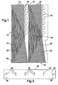
- Fig. 1 illustrates a magnified view of a portion of the charge plate fan out pattern 10, particularly showing how leads 12 are fanned out to two rows 14 and 16 of contacts with associated connector pads 18.
- Diagonal traces 20 shown at the bottom of Fig. 1 are at the density of the output leads from high voltage charge driver chips.
- the width required for the fan out of a group of leads going to a single row of contacts is equal to the width of the output leads at the driver chips.
- the subject invention allows the spacing of contacts to be increased without requiring excessive depth (front to back distance) of the charge plate.
- One preferred embodiment utilizes small alignment holes in the charge plate and the flex cable.
- a clamping bar (not shown) contains two alignment pins. These pins engage alignment holes of both the charge plate and the flex cable to maintain the registration of the two components.
- One set of alignment features can be used to align a multitude of the rows of contacts.
- a preferred embodiment uses one set of alignment features to register 20 rows of contacts, each row having 27 contacts.
- alignment holes 32 for the charge plate are machined into ceramic charge plate base 28, prior to laminating the electroformed charge plate coupon to the base.
- alignment holes 32 in the charge plate there are through holes 30 machined into the ceramic for receiving clamping screws.
- alignment features 26 in the coupon and the base there are additional alignment features 26 in the coupon and the base to ensure the proper alignment of the charge plate lead pattern with the machined alignment holes 30 in the charge plate base.
- the charge electrode leads are defined via photolithography, therefore insuring accurate location of the leads in relation to the alignment holes of the electroformed coupon.
- electrical connections can be made using a variety of processes. These include processes such as soldering or using conductive epoxy, where a solder paste or epoxy is applied to the charge plate using a stencil or screen printing process. Anisotropic conductive film adhesives can also be employed. Of course, each of the preceding processes are somewhat permanent in nature, not allowing the charge plate and the flex cable to be separated without causing damage to one or both components.
- the raised contacts for the interconnect pad region can either be located on the flex cable or the charge plate.
- Raised contacts on the flex cable and methods for making the same are well known in the art. Some of these processes, however, require large clamping forces, as many as 100 gram-force per contact, which is undesirable, as being capable of causing mechanical stress and deformation of the catcher component. Other configurations of raised bumps require much lower contact forces, in the range of 25-40 gram-force per contact. These produce minimal deformation of the catcher component. Therefore, care must be taken in the choice and design of pressure-based interconnects to keep the contact forces to a minimum, as excessive contact forces can cause the catcher and charge plate to deform.
- a metal plate is compressed against a formed elastomeric pad which is in contact with the flex circuit containing the raised interconnect pads.
- the elastomeric pad contains discrete protrusions which concentrates the pressure at the interconnect pad locations on the flex circuit.
- This plate and elastomeric pad can be combined into what is known as an elastomeric clamping mechanism.
- the clamping mechanism is compressed against the flex circuit by means of screws. On the charge plate connection, these screws pass through the through holes 30 in the charge plate and are screwed into the catcher underneath the charge plate. In this connection, the catcher is acting as a mechanical stiffener to ensure the contact area remains planar and that all the contacts receive an equivalent amount of pressure.
- the charge driver board connection involves the screws passing through clearance holes in the printed circuit board and screwing into an external plate known as a stiffener on the opposite side.
- the pressure connection may utilize anisotropic conductive elastomers to provide the electrical connection.
- the elastomer is placed between the charge plate and the mating circuit (flex circuit). Conductive fillers in the material provide electrical contact between the charge plate and the mating circuit while maintaining isolation between adjacent electrodes of the charge plate.
- the anisotropic conductive elastomers are compliant, the clamping mechanism does not require an elastomeric pad to distribute the clamping force.
Landscapes
- Ink Jet (AREA)
- Particle Formation And Scattering Control In Inkjet Printers (AREA)
Description
- The present invention relates to continuous ink-jet printers and, more particularly, to a compact, high density electrical interconnect system for a continuous ink jet printhead.
- In continuous ink jet printing, electrically conductive ink is transferred under pressure to a manifold. The orifices are arranged along this manifold in a linear array(s). The electrically conductive ink discharges from orifices in filaments. These filaments become streams of ink droplets. At the point the droplet stream breaks free from the filament, selected droplets are charged. In order for the droplets of ink to be properly charged, the break off of the drop must be in front of the charging electrode. These charged droplets are deflected away from their normal trajectory. They are caught or attracted to a conductive surface and recirculated. The uncharged droplets proceed in a path to the print medium.
- The current method of drop charging and deflection in state-of-the-art printheads relies on what is known as planar charging technology. This method involves a series of electrically grounded ink-jets forming droplets at a controlled distance from the orifice plate. A parallel array of charging electrodes is aligned to the ink jets. Each of these charging electrodes must be individually connected to a separate output lead from the high voltage charge driver chips, which control the charging electrodes. Different methods for providing a compact electrical interconnect between high voltage driver chips and the associated charging electrodes have been employed in certain state-of-the-art printheads, such as those manufactured by Scitex Digital Printing, Inc., in Dayton, Ohio. In each case the density at which the interconnection can be made determines the physical size of the printhead. As the width and print density (dpi) of the printheads increase, the number of interconnects also increases proportionally. Since there is always a need for printheads with a small "footprint" (i.e., small outer dimensions), the interconnect density has been kept as small as possible.
- In several prior art printers, charging electrodes which had a pitch of 610 electrodes per cm (240 electrodes per inch) were fanned out to 254 leads per cm (100 leads per inch) for connection with a flex circuit. In the flex circuit, the lead spacings were further increased to allow connections to be made to commercially available connectors. See for example EP-A-0 671 269 (Domino Printing Sciences PLC) 13 September 1995. Even at the fanned out spacing of 254 leads per cm (100 connections per inch) at the flex cable, it has been difficult to make the interconnects reliably. Further reductions in the interconnect density will be difficult to achieve as the technologies required, such as soldering, anisotropic adhesives, flex circuits, and printed circuit board fabrication, have already been pushed to their limits.
- For a charge plate such as is shown in U.S. Patent No. 4,560,991, the charge plate width would need to be 2.4 times wider than the ink jet array width to provide the necessary interconnects. For a long array printhead this excess width is not feasible. U.S. Patent No. 5,475,409 illustrates a more compact interconnect. Connections are made between the charge plate and several flex cables. The contacts for each flex cable are in a linear array, with the array oriented perpendicular to the jet array. This configuration adds to the required depth of the charge plate but greatly reduces the width requirement. However, it is still necessary for the leads to be shifted over to provide the room for each linear array of contacts. For this prior art, the required shift is about 0.318cm (0.125 inches) for every 64 connection linear array. Therefore, for an approximately 10cm (4") array at 610 jets per cm (240 jets per inch), the configuration required a charge plate width of about 14cm (5.5"). This is a charge plate width over 35% wider than the jet array. For longer arrays, this configuration becomes unacceptable. For printheads with more jets per centimeter (inch), the problem becomes worse.
- In another prior art configuration, the leads from the charging electrodes were fanned out to wire bond connections directly to the charge driver dies. This allowed for a reduced printhead size by eliminating much of the need to fan out the interconnects. This technique, however, has proven to be costly. With the charge driver electronics attached directly onto the charge plate, both the charge plate and the driver electronics must be scrapped if one of the component fails. With longer arrays having a large number of charge driver electronics, the scrap costs can be excessive.
- With the need for longer ink jet arrays with higher print densities and the concurrent need for minimal overall size of the printhead, it is seen that there is a need for an improved charge plate configuration. A preferred charge plate design would allow interconnects to be made reliably, and preferably using a system which allows the components to be salvaged, in the event of a failure. See US-A-4,347,522 (Bahl surinder K et al.) 31 August 1982, which discloses a charge plate having charging electrodes terminating at contact pads, a mating circuit, alignment features such as holes through the charge plate and mating circuit, and mechanically engagement of the alignment features by means of screws.
- The problems associated with prior art interconnect systems are overcome by the charge plate according to claim 1, wherein a lead fan out configuration is proposed, having regions with a higher trace density than the charging electrode density on the charge plate face and terminating in a two dimensional array of contact pads per connector at spacings which are common in the electronics industry. By having a more common electrical interconnect pitch and alignment features in the charge plate and mating flex cable, the two components are self aligning. A clamping means which attaches to the charge plate maintains the alignment of the components and provides the pressure needed to insure electrical contact. In accordance with one aspect of the present invention, a system and method for establishing a high-density electrical interconnection between high-voltage driver chips and charging electrodes controlled by the driver chips. A charge plate having charging electrodes on its face, connected to an array of contact pads. Alignment features are then provided on the charge plate and/or the mating circuit. The alignment features of the charge plate and the mating circuit are mechanically engaged to ensure alignment of mating contact pads. And an interconnect is provided for the aligned mating contact pads.
- The present invention establishes a high-density electrical interconnection between the high-voltage driver chips and the charging electrodes controlled by the driver chips, for a continuous ink jet printhead.
- Other objects and advantages of the invention will be apparent from the following description and the appended claims.
-
- Fig. 1 illustrates a magnified view of a portion of a charge plate fan out pattern, in accordance with the present invention; and
- Fig. 2 illustrates an alignment configuration for the interconnect system of Fig. 1, in accordance with the present invention.
- As discussed above, charge plates made per the processes defined in patents 4,560,991 or 5,512,117 require the lead structure to be formed by an electroforming process. This electroforming process produces an excessive number of failures when the line widths or the spaces are less than about 0.05mm (2 mils) each. The failures are either opens in a conductive lead or lead to lead shorts.
- Advances in charge plate circuitry fabrication facilitate the use of finer lines and spaces than before. The recent advances allow line widths and spaces to be reduced to about 0.025mm (1 mil). Even with an increase in jet array density to 762 jets per centimeter (300 jets per inch) (a pitch of 0.08mm (3.3 mil)), this new process allows the lead density to be higher than the charging electrode density. By going to a higher density of leads, it is possible to free up space for a row of connection pads without requiring extra width.
- Referring now to the drawings, Fig. 1 illustrates a magnified view of a portion of the charge plate fan out
pattern 10, particularly showing how leads 12 are fanned out to tworows connector pads 18.Diagonal traces 20 shown at the bottom of Fig. 1 are at the density of the output leads from high voltage charge driver chips.Bend 22 in thepattern 10, formingvertical section 24, reduces the line width and spacings. This reduction in the width of a group of leads provides enough space for thecontact pads 18 and a clearance area around each pad. As such, in accordance with the configuration of the present invention, the width required for the fan out of a group of leads going to a single row of contacts is equal to the width of the output leads at the driver chips. - As there is no extra width required for a line of contacts pads when configured according to the present invention, a large number of rows of contacts can therefore be used. Furthermore, since the space required to fan the leads out to the rows of contacts is so compact, the subject invention allows the spacing of contacts to be increased without requiring excessive depth (front to back distance) of the charge plate.
- At a spacing of contacts of 0.064mm (25 mil), which is common in the electronics industry, it is now no longer necessary to optically align the contact pads of the charge plate and the mating flex cable. Rather, alignment features of the present invention can be fabricated into each component to insure alignment.
- One preferred embodiment utilizes small alignment holes in the charge plate and the flex cable. A clamping bar (not shown) contains two alignment pins. These pins engage alignment holes of both the charge plate and the flex cable to maintain the registration of the two components. One set of alignment features can be used to align a multitude of the rows of contacts. A preferred embodiment, by way of example only, uses one set of alignment features to register 20 rows of contacts, each row having 27 contacts.
- Referring now to Fig. 2, alignment holes 32 for the charge plate are machined into ceramic
charge plate base 28, prior to laminating the electroformed charge plate coupon to the base. In addition to these alignment holes 32 in the charge plate, there are throughholes 30 machined into the ceramic for receiving clamping screws. There are additional alignment features 26 in the coupon and the base to ensure the proper alignment of the charge plate lead pattern with the machined alignment holes 30 in the charge plate base. As in the flex circuit, the charge electrode leads are defined via photolithography, therefore insuring accurate location of the leads in relation to the alignment holes of the electroformed coupon. - With the contact pads of the charge plate and the mating circuit aligned by means of alignment features on both parts, electrical connections can be made using a variety of processes. These include processes such as soldering or using conductive epoxy, where a solder paste or epoxy is applied to the charge plate using a stencil or screen printing process. Anisotropic conductive film adhesives can also be employed. Of course, each of the preceding processes are somewhat permanent in nature, not allowing the charge plate and the flex cable to be separated without causing damage to one or both components.
- In addition to these processes, there are various processes which utilize pressure to hold the components together to make the electrical contacts. These processes are more desirable in the art, as such processes do not damage either the charge plate or the mating circuit, allowing the system to be more effectively refurbished and reused. These pressure related processes include the use of raised contacts and/or anisotropic conductive elastomers.
- By raising the contact pads for the interconnect above the plane of the substrate, clamping forces can be concentrated at the contacts, helping to ensure electrical contact. The raised contacts for the interconnect pad region can either be located on the flex cable or the charge plate. Raised contacts on the flex cable and methods for making the same are well known in the art. Some of these processes, however, require large clamping forces, as many as 100 gram-force per contact, which is undesirable, as being capable of causing mechanical stress and deformation of the catcher component. Other configurations of raised bumps require much lower contact forces, in the range of 25-40 gram-force per contact. These produce minimal deformation of the catcher component. Therefore, care must be taken in the choice and design of pressure-based interconnects to keep the contact forces to a minimum, as excessive contact forces can cause the catcher and charge plate to deform.
- To provide and distribute the necessary pressure to raised contact pads, a metal plate is compressed against a formed elastomeric pad which is in contact with the flex circuit containing the raised interconnect pads. The elastomeric pad contains discrete protrusions which concentrates the pressure at the interconnect pad locations on the flex circuit. This plate and elastomeric pad can be combined into what is known as an elastomeric clamping mechanism. The clamping mechanism is compressed against the flex circuit by means of screws. On the charge plate connection, these screws pass through the through
holes 30 in the charge plate and are screwed into the catcher underneath the charge plate. In this connection, the catcher is acting as a mechanical stiffener to ensure the contact area remains planar and that all the contacts receive an equivalent amount of pressure. The charge driver board connection involves the screws passing through clearance holes in the printed circuit board and screwing into an external plate known as a stiffener on the opposite side. - Alternatively, the pressure connection may utilize anisotropic conductive elastomers to provide the electrical connection. The elastomer is placed between the charge plate and the mating circuit (flex circuit). Conductive fillers in the material provide electrical contact between the charge plate and the mating circuit while maintaining isolation between adjacent electrodes of the charge plate. As the anisotropic conductive elastomers are compliant, the clamping mechanism does not require an elastomeric pad to distribute the clamping force.
- While the description herein has described a single set of connections having a compression pad, it will be understood that a multitude of connectors can be used, each with a two dimensional array of contacts, alignment means to register the contacts and means to maintain electrical connection, all without departing from the invention. A preferred embodiment of the present invention, however, uses five connectors, each with 540 electrical contacts.
Claims (6)
- , An improved charge plate (10) for individually connecting ink jet printer charging electrodes to a separate output lead of a charge driver chip for controlling the charging electrodes; the charge plate (10) having an array of charging electrode contact pads (18) respectively associated with the charging electrodes, a trace pattern of electrical leads (12, 14, 16, 20, 22, 24) respectively associated with the output leads of the charge driver chip, characterized in that the trace pattern of electrical leads fans out from the array of contact pads (18) to form a configuration of electrical leads (12, 14, 16, 20, 22, 24) having regions of trace density higher than the density of the array of charging electrode contact pads.
- An improved charge plate as claimed in claim 1 wherein the trace pattern of electrical leads terminates in a two-dimensional linear array of contact pads for connection to the output leads of the charge driver chip.
- An improved charge plate as claimed in claim 2 wherein the array of charging electrode contact pads (18) is linear and is aligned generally normal to the linear array of contact pads for connection to the output leads of the charge driver chip.
- An improved charge plate as claimed in claim 3 wherein the array of charging electrode contact pads (18) is aligned generally parallel to the trace pattern of electrical leads.
- An improved charge plate as claimed in claim 4 wherein the array of charging electrode contact pads (18) is adjacent to the trace pattern of electrical leads.
- An improved charge plate as claimed in claim 5 wherein the combined width of the array of charging electrode contact pads (18) and the trace pattern of electrical leads is no greater than the width of the array of contact pads for connection to the output leads of the charge driver chip.
Applications Claiming Priority (2)
| Application Number | Priority Date | Filing Date | Title |
|---|---|---|---|
| US21121298A | 1998-12-14 | 1998-12-14 | |
| US211212 | 1998-12-14 |
Publications (3)
| Publication Number | Publication Date |
|---|---|
| EP1013430A2 EP1013430A2 (en) | 2000-06-28 |
| EP1013430A3 EP1013430A3 (en) | 2001-04-04 |
| EP1013430B1 true EP1013430B1 (en) | 2006-06-14 |
Family
ID=22785989
Family Applications (1)
| Application Number | Title | Priority Date | Filing Date |
|---|---|---|---|
| EP19990309493 Expired - Lifetime EP1013430B1 (en) | 1998-12-14 | 1999-11-29 | High density electrical interconnect for a continuous ink jet printhead |
Country Status (4)
| Country | Link |
|---|---|
| EP (1) | EP1013430B1 (en) |
| JP (1) | JP2000218795A (en) |
| CA (1) | CA2292082A1 (en) |
| DE (1) | DE69931880T2 (en) |
Families Citing this family (1)
| Publication number | Priority date | Publication date | Assignee | Title |
|---|---|---|---|---|
| WO2016176692A2 (en) * | 2016-06-17 | 2016-11-03 | Ohmx Corporation | Biosensor chip |
Family Cites Families (6)
| Publication number | Priority date | Publication date | Assignee | Title |
|---|---|---|---|---|
| US4047184A (en) * | 1976-01-28 | 1977-09-06 | International Business Machines Corporation | Charge electrode array and combination for ink jet printing and method of manufacture |
| US4347522A (en) * | 1981-04-01 | 1982-08-31 | The Mead Corporation | Laminated metal charge plate |
| US4560991A (en) | 1983-07-27 | 1985-12-24 | Eastman Kodak Company | Electroformed charge electrode structure for ink jet printers |
| US4774527A (en) * | 1987-01-07 | 1988-09-27 | International Business Machines Corporation | Printhead having electrodes at more than one edge surface |
| US5475409A (en) | 1992-05-29 | 1995-12-12 | Scitex Digital Printing, Inc. | Alignment structure for components of an ink jet print head |
| GB9404741D0 (en) * | 1994-03-10 | 1994-04-27 | Domino Printing Sciences Plc | Electrode assembly for a continuous ink jet printer |
-
1999
- 1999-11-29 EP EP19990309493 patent/EP1013430B1/en not_active Expired - Lifetime
- 1999-11-29 DE DE69931880T patent/DE69931880T2/en not_active Expired - Lifetime
- 1999-12-10 CA CA 2292082 patent/CA2292082A1/en not_active Abandoned
- 1999-12-13 JP JP35300499A patent/JP2000218795A/en active Pending
Also Published As
| Publication number | Publication date |
|---|---|
| EP1013430A2 (en) | 2000-06-28 |
| EP1013430A3 (en) | 2001-04-04 |
| CA2292082A1 (en) | 2000-06-14 |
| DE69931880T2 (en) | 2007-05-31 |
| JP2000218795A (en) | 2000-08-08 |
| DE69931880D1 (en) | 2006-07-27 |
Similar Documents
| Publication | Publication Date | Title |
|---|---|---|
| US5850240A (en) | Arrangement for an ink-jet printer head composed of individual ink printer modules | |
| US7570494B2 (en) | Structure of flexible printed circuit board | |
| EP0654958B1 (en) | Tab circuit fusible links for disconnection or encoding information | |
| US6705705B2 (en) | Substrate for fluid ejection devices | |
| EP0289347A2 (en) | Thermal ink jet print head | |
| US6824254B2 (en) | Multi-nozzle ink jet head and manufacturing method thereof | |
| EP0410656A1 (en) | Electrical make/break interconnect having high trace density | |
| US10814616B2 (en) | Inkjet head, inkjet printer, and manufacturing method for inkjet head | |
| US6464333B1 (en) | Inkjet printhead assembly with hybrid carrier for printhead dies | |
| US6543885B2 (en) | Ink jet charge plate with integrated flexible lead connector structure | |
| EP0268395A2 (en) | Print head for ink jet printer | |
| US5870118A (en) | Ink-jet printer head formed of multiple ink-jet printer modules | |
| US7338152B2 (en) | Inkjet head | |
| CN110962457B (en) | Liquid ejection head | |
| US6274057B1 (en) | Method for etch formation of electrical contact posts on a charge plate used for ink jet printing | |
| EP1013430A2 (en) | High density electrical interconnect for a continuous ink jet printhead | |
| US20080128159A1 (en) | Method for manufacturing a printed circuit board that mounts an integrated circuit device thereon and the printed circuit board | |
| US5801734A (en) | Two row flat face charging for high resolution printing | |
| JP7520666B2 (en) | LIQUID JET HEAD AND LIQUID JET RECORDING APPARATUS | |
| JP2025184364A (en) | Circuit board, liquid jet head, and liquid jet recording apparatus | |
| JP2025111226A (en) | Flexible substrate, liquid jet head and liquid jet recording apparatus | |
| JP3690031B2 (en) | Inkjet recording head | |
| JP2020055296A (en) | Liquid ejection head | |
| JP2002216872A (en) | Printhead for inkjet |
Legal Events
| Date | Code | Title | Description |
|---|---|---|---|
| PUAI | Public reference made under article 153(3) epc to a published international application that has entered the european phase |
Free format text: ORIGINAL CODE: 0009012 |
|
| AK | Designated contracting states |
Kind code of ref document: A2 Designated state(s): DE FR GB |
|
| AX | Request for extension of the european patent |
Free format text: AL;LT;LV;MK;RO;SI |
|
| PUAL | Search report despatched |
Free format text: ORIGINAL CODE: 0009013 |
|
| AK | Designated contracting states |
Kind code of ref document: A3 Designated state(s): AT BE CH CY DE DK ES FI FR GB GR IE IT LI LU MC NL PT SE |
|
| AX | Request for extension of the european patent |
Free format text: AL;LT;LV;MK;RO;SI |
|
| RIC1 | Information provided on ipc code assigned before grant |
Free format text: 7B 41J 2/14 A, 7B 41J 2/02 B, 7B 41J 2/085 B |
|
| 17P | Request for examination filed |
Effective date: 20010924 |
|
| AKX | Designation fees paid |
Free format text: DE FR GB |
|
| RAP1 | Party data changed (applicant data changed or rights of an application transferred) |
Owner name: EASTMAN KODAK COMPANY |
|
| 17Q | First examination report despatched |
Effective date: 20041126 |
|
| GRAP | Despatch of communication of intention to grant a patent |
Free format text: ORIGINAL CODE: EPIDOSNIGR1 |
|
| GRAS | Grant fee paid |
Free format text: ORIGINAL CODE: EPIDOSNIGR3 |
|
| GRAA | (expected) grant |
Free format text: ORIGINAL CODE: 0009210 |
|
| AK | Designated contracting states |
Kind code of ref document: B1 Designated state(s): DE FR GB |
|
| REG | Reference to a national code |
Ref country code: GB Ref legal event code: FG4D |
|
| REF | Corresponds to: |
Ref document number: 69931880 Country of ref document: DE Date of ref document: 20060727 Kind code of ref document: P |
|
| ET | Fr: translation filed | ||
| PLBE | No opposition filed within time limit |
Free format text: ORIGINAL CODE: 0009261 |
|
| STAA | Information on the status of an ep patent application or granted ep patent |
Free format text: STATUS: NO OPPOSITION FILED WITHIN TIME LIMIT |
|
| 26N | No opposition filed |
Effective date: 20070315 |
|
| PGFP | Annual fee paid to national office [announced via postgrant information from national office to epo] |
Ref country code: GB Payment date: 20101022 Year of fee payment: 12 |
|
| PGFP | Annual fee paid to national office [announced via postgrant information from national office to epo] |
Ref country code: FR Payment date: 20111103 Year of fee payment: 13 |
|
| PGFP | Annual fee paid to national office [announced via postgrant information from national office to epo] |
Ref country code: DE Payment date: 20111130 Year of fee payment: 13 |
|
| GBPC | Gb: european patent ceased through non-payment of renewal fee |
Effective date: 20121129 |
|
| REG | Reference to a national code |
Ref country code: FR Ref legal event code: ST Effective date: 20130731 |
|
| REG | Reference to a national code |
Ref country code: DE Ref legal event code: R119 Ref document number: 69931880 Country of ref document: DE Effective date: 20130601 |
|
| PG25 | Lapsed in a contracting state [announced via postgrant information from national office to epo] |
Ref country code: DE Free format text: LAPSE BECAUSE OF NON-PAYMENT OF DUE FEES Effective date: 20130601 |
|
| PG25 | Lapsed in a contracting state [announced via postgrant information from national office to epo] |
Ref country code: GB Free format text: LAPSE BECAUSE OF NON-PAYMENT OF DUE FEES Effective date: 20121129 Ref country code: FR Free format text: LAPSE BECAUSE OF NON-PAYMENT OF DUE FEES Effective date: 20121130 |