EP1012888B1 - Method for fabricating fbars on glass substrates - Google Patents
Method for fabricating fbars on glass substrates Download PDFInfo
- Publication number
- EP1012888B1 EP1012888B1 EP97941066A EP97941066A EP1012888B1 EP 1012888 B1 EP1012888 B1 EP 1012888B1 EP 97941066 A EP97941066 A EP 97941066A EP 97941066 A EP97941066 A EP 97941066A EP 1012888 B1 EP1012888 B1 EP 1012888B1
- Authority
- EP
- European Patent Office
- Prior art keywords
- set forth
- sacrificial layer
- layer
- substrate
- polymer
- Prior art date
- Legal status (The legal status is an assumption and is not a legal conclusion. Google has not performed a legal analysis and makes no representation as to the accuracy of the status listed.)
- Expired - Lifetime
Links
Images

Classifications
-
- H—ELECTRICITY
- H03—ELECTRONIC CIRCUITRY
- H03H—IMPEDANCE NETWORKS, e.g. RESONANT CIRCUITS; RESONATORS
- H03H9/00—Networks comprising electromechanical or electro-acoustic elements; Electromechanical resonators
- H03H9/15—Constructional features of resonators consisting of piezoelectric or electrostrictive material
- H03H9/17—Constructional features of resonators consisting of piezoelectric or electrostrictive material having a single resonator
- H03H9/171—Constructional features of resonators consisting of piezoelectric or electrostrictive material having a single resonator implemented with thin-film techniques, i.e. of the film bulk acoustic resonator [FBAR] type
- H03H9/172—Means for mounting on a substrate, i.e. means constituting the material interface confining the waves to a volume
- H03H9/173—Air-gaps
-
- H—ELECTRICITY
- H03—ELECTRONIC CIRCUITRY
- H03H—IMPEDANCE NETWORKS, e.g. RESONANT CIRCUITS; RESONATORS
- H03H3/00—Apparatus or processes specially adapted for the manufacture of impedance networks, resonating circuits, resonators
- H03H3/007—Apparatus or processes specially adapted for the manufacture of impedance networks, resonating circuits, resonators for the manufacture of electromechanical resonators or networks
- H03H3/02—Apparatus or processes specially adapted for the manufacture of impedance networks, resonating circuits, resonators for the manufacture of electromechanical resonators or networks for the manufacture of piezoelectric or electrostrictive resonators or networks
- H03H2003/021—Apparatus or processes specially adapted for the manufacture of impedance networks, resonating circuits, resonators for the manufacture of electromechanical resonators or networks for the manufacture of piezoelectric or electrostrictive resonators or networks the resonators or networks being of the air-gap type
-
- Y—GENERAL TAGGING OF NEW TECHNOLOGICAL DEVELOPMENTS; GENERAL TAGGING OF CROSS-SECTIONAL TECHNOLOGIES SPANNING OVER SEVERAL SECTIONS OF THE IPC; TECHNICAL SUBJECTS COVERED BY FORMER USPC CROSS-REFERENCE ART COLLECTIONS [XRACs] AND DIGESTS
- Y10—TECHNICAL SUBJECTS COVERED BY FORMER USPC
- Y10T—TECHNICAL SUBJECTS COVERED BY FORMER US CLASSIFICATION
- Y10T29/00—Metal working
- Y10T29/42—Piezoelectric device making
-
- Y—GENERAL TAGGING OF NEW TECHNOLOGICAL DEVELOPMENTS; GENERAL TAGGING OF CROSS-SECTIONAL TECHNOLOGIES SPANNING OVER SEVERAL SECTIONS OF THE IPC; TECHNICAL SUBJECTS COVERED BY FORMER USPC CROSS-REFERENCE ART COLLECTIONS [XRACs] AND DIGESTS
- Y10—TECHNICAL SUBJECTS COVERED BY FORMER USPC
- Y10T—TECHNICAL SUBJECTS COVERED BY FORMER US CLASSIFICATION
- Y10T29/00—Metal working
- Y10T29/49—Method of mechanical manufacture
- Y10T29/49002—Electrical device making
- Y10T29/49005—Acoustic transducer
-
- Y—GENERAL TAGGING OF NEW TECHNOLOGICAL DEVELOPMENTS; GENERAL TAGGING OF CROSS-SECTIONAL TECHNOLOGIES SPANNING OVER SEVERAL SECTIONS OF THE IPC; TECHNICAL SUBJECTS COVERED BY FORMER USPC CROSS-REFERENCE ART COLLECTIONS [XRACs] AND DIGESTS
- Y10—TECHNICAL SUBJECTS COVERED BY FORMER USPC
- Y10T—TECHNICAL SUBJECTS COVERED BY FORMER US CLASSIFICATION
- Y10T29/00—Metal working
- Y10T29/49—Method of mechanical manufacture
- Y10T29/49002—Electrical device making
- Y10T29/49117—Conductor or circuit manufacturing
- Y10T29/49124—On flat or curved insulated base, e.g., printed circuit, etc.
- Y10T29/49155—Manufacturing circuit on or in base
- Y10T29/49156—Manufacturing circuit on or in base with selective destruction of conductive paths
-
- Y—GENERAL TAGGING OF NEW TECHNOLOGICAL DEVELOPMENTS; GENERAL TAGGING OF CROSS-SECTIONAL TECHNOLOGIES SPANNING OVER SEVERAL SECTIONS OF THE IPC; TECHNICAL SUBJECTS COVERED BY FORMER USPC CROSS-REFERENCE ART COLLECTIONS [XRACs] AND DIGESTS
- Y10—TECHNICAL SUBJECTS COVERED BY FORMER USPC
- Y10T—TECHNICAL SUBJECTS COVERED BY FORMER US CLASSIFICATION
- Y10T29/00—Metal working
- Y10T29/49—Method of mechanical manufacture
- Y10T29/49002—Electrical device making
- Y10T29/49117—Conductor or circuit manufacturing
- Y10T29/49124—On flat or curved insulated base, e.g., printed circuit, etc.
- Y10T29/49155—Manufacturing circuit on or in base
- Y10T29/49165—Manufacturing circuit on or in base by forming conductive walled aperture in base
Definitions
- the invention relates to resonators and, in particular, the invention relates to a method for fabricating Thin Film Bulk Acoustic Wave Resonators (FBARs).
- FBARs Thin Film Bulk Acoustic Wave Resonators
- FBARs Thin Film Bulk Acoustic Wave Resonators
- semiconductor wafers including those which are comprised of Silicon (Si) or gallium arsenide (GaAs).
- Si Silicon
- GaAs gallium arsenide
- an acoustic bulk wave resonator which comprises a thin film piezoelectric layer of Zinc-Oxide (ZnO) sputtered over a thin membrane of Silicon (Si).
- semiconductor wafers and crystalline wafers need to be carefully polished after being cut from a crystal in order to smooth their surfaces.
- the polishing process can be expensive.
- a substrate that is formed of a low cost material and which exhibits a low permittivity characteristic and low parasitic capacitances. It would also be advantageous to provide a substrate that is formed of a material that does not need to be polished in order to smooth its surfaces.
- a multi-layered ultrasonic transducer which includes an air gap formed by the removal of a "sacrificial" ZnO layer.
- U.S. Pat. No. 4,642,508 to Suzuki et al entitled “Piezoelectric Resonating Device”, also describes a thin film resonator where an air gap between the substrate and a SiO 2 film layer that supports a piezoelectric layer is formed by disposing ZnO and dissolving it with a dilute acid to leave the air gap.
- a sacrificial layer of ZnO is deposited (e.g., sputtered) over a substrate.
- the sacrificial layer is later removed via an etching step that is performed after all of the layers of the FBAR have been completely formed.
- One drawback of this process is that the steps of sputtering and forming the sacrificial layer can be tedious and time-consuming. This is because ZnO is a ceramic material, and thus is brittle and has a low thermal conductivity. If, by example, very high power is employed during the sputtering of the ZnO, the "target" substrate may break. Also, the growth rate of the ZnO must be controlled to produce a correct crystal orientation and crystallite size distribution. Thus, the growth rate may need to be limited to only 2 ⁇ m/h.
- a sacrificial layer formed of ZnO is that the surface of the crystalline ZnO film is textured, and thus causes acoustic energy scattering losses to occur within the FBAR. Also, the textured surface of the ZnO may cause the surface of a layer (e.g., the bridge layer) formed over the sacrificial ZnO layer to become deformed.
- a sacrificial layer of ZnO is that during the etching of the layer to form an air gap, a piezoelectric ZnO layer that is formed on the sacrificial layer can become damaged.
- FBAR Thin Film Bulk Acoustic Wave Resonator
- FBAR Thin Film Bulk Acoustic Wave Resonator
- FBAR Thin Film Bulk Acoustic Wave Resonator
- FBAR Thin Film Bulk Acoustic Wave Resonator
- the method of the present invention employs a sacrificial layer that is comprised of either a metal or polymer material instead of a conventionally-used material such as, by example, zinc-oxide (ZnO).
- ZnO zinc-oxide
- a first step includes sputtering a metal such as, by example copper (Cu) over a substrate.
- a metal such as, by example copper (Cu)
- the sputtered Cu is then patterned to form a sacrificial layer.
- a next step includes depositing silicon dioxide (SiO 2 ) over the sacrificial layer and over selected portions of the substrate to form a first SiO 2 layer (also referred to as a "first protective layer").
- This layer may not be needed in cases in which the piezoelectric layer comprises a material which will not be detrimentally affected by the etching of the sacrificial layer (which will be described below).
- a metallic material such as, by example, gold (Au) is deposited over a selected portion of the first SiO 2 layer. The deposited gold is then patterned to form a bottom electrode layer.
- a next step includes depositing zinc-oxide (ZnO) over a selected portion of the bottom electrode layer, and over a selected portion of the first SiO 2 layer.
- ZnO zinc-oxide
- the ZnO is then patterned to form a ZnO layer (also referred to as a "piezoelectric layer").
- a next step of the process includes depositing a further metallic material such as, by example, gold, over a selected portion of the ZnO layer. Thereafter, the deposited gold is patterned to form a top electrode layer.
- a second protective layer may also be formed on the structure to protect the piezoelectric layer during the formation of the vias and/or during the etching of the sacrificial layer which will be described below.
- Vias are then formed in the structure so that the sacrificial layer can be removed. Thereafter, the sacrificial layer is removed through the vias to form an air gap.
- the fabrication process of the invention may also be performed using a sacrificial layer that is comprised of a polymer instead of a metal.
- the steps of this process are similar to those described above, except that the steps of depositing, patterning, and removing the sacrificial layer (e.g., the polymer) are performed in a different manner.
- the step of depositing the polymer is performed by spinning the polymer onto the substrate. The polymer is then patterned to form the sacrificial layer. After each of the other layers and the vias of the FBAR have been formed in the same manner as described above, the sacrificial layer is removed to form the air gap.
- the type of polymer used to form the sacrificial layer is preferably one that can withstand the high temperatures that can be reached during the sputtering of the ZnO layer.
- the method for fabricating FBARs may be performed by removing the sacrificial layer prior to the deposition of the material forming the ZnO layer.
- the same steps described above are performed, except that after the first SiO 2 layer and the bottom electrode layer have been formed, the sacrificial layer is then removed to form the air gap in the same manner as described above. Thereafter, the steps of forming the ZnO layer and the top electrode layer are carried out in the same manner as described above.
- metals and polymers to form sacrificial layers has many advantages over the use of most conventionally-used materials including, by example, ZnO.
- FBARs having sacrificial layers that are comprised of metals or polymers can be fabricated more quickly than the FBARs having sacrificial layers formed of ZnO.
- metals and polymers generally have smoother surfaces than ZnO.
- metals and polymers can be etched using chemicals that are not harmful to piezoelectric layers formed of, by example, ZnO.
- an FBAR which includes a glass substrate.
- the FBAR is formed of similar layers as the FBARs described above, and may be fabricated in accordance with the method of the invention.
- the use of glass to form substrates offers several advantages over the use of other materials to form substrates. Glass is inexpensive and thus can be used to form substrates having large surface areas at an inexpensive cost. Also, most glass materials exhibit low permittivity characteristics and low parasitic capacitances. Moreover, most glass materials become substantially loss free when used in microwave frequency applications.
- a further advantage of using glass to form substrates is that, unlike semiconductor materials, glass can have inherently smooth surfaces and thus requires little or no polishing.
- FBARs Thin Film Bulk Acoustic Wave Resonators
- ZnO zinc-oxide
- the method of the present invention employs a sacrificial layer that is comprised of either a metal or a polymer material.
- the use of these materials to form sacrificial layers has many advantages over the use of ZnO to form these layers, as will be described below.
- a metal such as, by example, copper (Cu) is sputtered or otherwise deposited over a substrate 42. It is assumed that the substrate is comprised of glass, in accordance with an aspect of this invention which will be further described below, although any other suitable solid material may be employed.
- the sputtered Cu is then patterned so that it has a thickness of, by example, approximately 2000nm, thereby forming bridges.
- a sacrificial layer also referred to as a "base layer” 44 is formed.
- the sacrificial layer 44 may be formed of aluminum, zinc, antimony, and any of the elements in the periodic table extending from titanium to copper, from yttrium to silver, and from lanthanum to gold. Ideally, the metals used to form the layer 44 are low cost and can be etched without great difficulty.
- a next step includes depositing silicon-dioxide (SiO 2 ) over the sacrificial layer 44 and over selected portions of the substrate 42 to form a first SiO 2 layer (also referred to as a "first protective layer") 48 having a thickness of, by example, approximately 300nm.
- a metallic material such as, by example, gold (Au) is deposited over a selected portion of the first SiO 2 layer 48.
- the deposited gold is then patterned to form a bottom electrode layer 50 having a thickness of, by example, approximately 300 nm.
- Other suitable electrically conductive metallic and non-metallic materials can also be employed.
- the material used to form the piezoelectric layer (to be described below) is not detrimentally effected by the etching of the sacrificial layer (the etching of the sacrificial layer will be described below), it is not necessary to employ the first protective layer 48, and the bottom electrode layer may be formed directly over the sacrificial layer 44 and selected portions of the substrate 42.
- a next step includes depositing zinc-oxide (ZnO) over a selected portion of the bottom electrode layer 50, and over a selected portion of the first SiO 2 layer 48.
- the ZnO may be deposited by, for example, sputtering from a target in a mixture of Argon (Ar) and O 2 .
- Ar Argon
- O 2 Argon
- the ZnO is deposited, it is patterned to form a ZnO layer (also referred to as a "piezoelectric layer") 52 having a selected thickness (e.g., approximately 2000nm) that is a function of a desired resonant frequency of the FBAR.
- a next step of the process includes depositing a further metallic material such as, by example, gold, over a selected portion of the ZnO layer 52. Thereafter, the deposited gold is patterned to form a top electrode layer 54, which is illustrated in Fig. 5 .
- a further metallic material such as, by example, gold
- the deposited gold is patterned to form a top electrode layer 54, which is illustrated in Fig. 5 .
- other suitable electrically conductive metallic and non-metallic materials can also be employed.
- Vias are then formed in the structure so that the sacrificial layer 44 can be removed.
- the vias may be formed in any suitable manner. For example, and referring to Fig. 2a , selected portions of the first SiO2 layer 48 may be removed to provide openings 47 and 49 for accessing the sacrificial layer 44 (tapered edges 44a and 44b are shown). It should be noted that in cases where it is appropriate to protect the piezoelectric layer 52 during the creation of the vias and/or the removal of the sacrificial layer, a second layer of SiO 2 (also referred to as a "second protective layer”) (not illustrated in Fig. 2a ) may be employed.
- a second protective layer also referred to as a "second protective layer”
- SiO 2 may be deposited and patterned on a selected portion of the piezoelectric layer 52 after the piezoelectric layer 52 has been formed and before the top electrode layer 54 has been formed. The SiO 2 is then patterned to form a contact area on a top portion of the ZnO layer 52. Within the contact area the top electrode layer 54 is then formed. In other cases where it is appropriate, the second protective layer may instead be formed after the formation of the top electrode layer 54 on the piezoelectric layer 52.
- Vias may also be formed in the structure according to the example shown in Fig. 2b .
- holes may be formed in the ZnO layer 52 by an using an acid etchant.
- Selected portions of the FBAR and the surrounding wafer may then be covered by depositing a second protective layer of SiO 2 51 via, for example, a plasma-enhanced chemical vapor deposition (CVD).
- the SiO 2 is then patterned in fluorine plasma (F plasma) to form a contact area on a top portion of the ZnO layer 52.
- the top electrode layer 54 is formed over the contact area and over portions of the second layer of SiO 2 51.
- a next step of the fabrication process includes removing the sacrificial layer 44 through the vias by wet etching to form an air gap 62.
- the etching may be performed by using, for example, acids, alkalis, or redox reactions (e.g., ferric chloride). Either selective or non-selective etching may be used.
- the electrical performance characteristics of the device can then be measured in a suitable manner and compared with a model of the device.
- Any suitable technique may be employed for modeling the device including that disclosed in an article entitled "Systematic Design of Stacked-Crystal Filters by Microwave Network Methods", IEEE Trans. Microwave Theory Tech., vol. MTT-22, pp. 14-25, Jan. 1974, by Arthur Ballato, Henry L. Bertoni, and Theodor Tamir .
- Figs. 6a-8 illustrate steps of the fabrication process of the invention using a sacrificial layer that is formed of a polymer instead of a metal.
- the steps of this process are similar to those described above, except that the steps of depositing, patterning, and removing the sacrificial layer (e.g., the polymer) are performed in a different manner.
- the step of depositing the polymer is preferably performed by spinning the polymer onto the substrate 42 thereby providing an inherently smooth surface for further processing.
- the polymer is then patterned so that it has a thickness of, by example, approximately 1000nm, thereby forming bridges.
- the polymer is also etched to form tapered edges 44a and 44b in a similar manner as described above.
- sacrificial layer 60 is formed.
- the sacrificial layer 60 is then removed by, for example, etching or plasma aching. In this manner, air gap 62 is formed, which is illustrated in Fig. 8 .
- the sacrificial layer 60 can be etched in, by example, a plasma containing oxygen.
- a plasma containing oxygen for cases in which organic polymers are used to form the sacrificial layer 60
- silicone polymers for example, an addition of fluorine may be necessary.
- some types of polymers can be dissolved in organic solvents (e.g., acetone). Unlike the corrosive chemicals that are used for, by example, anisotropic etching of silicon, organic solvents do not attack ZnO. Thus, polymers which can be dissolved by organic solvents are preferred. Also, the use of this type of bridge structure avoids drawbacks that can be associated with the performance of, by example, deep anisotropic etching of silicon, which requires the etching of a large surface area because the etch stopping crystal plane is angled at, by example, only 54.74 degrees with respect to the surface of the wafer.
- organic solvents e.g., acetone
- the type of polymer used to form the sacrificial layer 60 is also preferably one that can withstand the high temperatures that can be reached during the sputtering of the ZnO layer 52.
- the polymer may be, by example, polytetrafluoroethylene or a derivative thereof, polyphenylene sulfide, polyetheretherketone, poly(para phenylene benzobismidazole), poly(para phenylene benzobisoxazole), poly (para phenylene benzobismidazole), poly (para phenylene benzobisthiazole), a polyimide, polyimide siloxane, vinyle ethers, polyphenyl, parylene-n, parylene-f, benzocyclobutene.
- the method for fabricating FBARs may be performed by removing the sacrificial layer prior to the deposition of the material forming the ZnO layer 52.
- the FBAR includes a sacrificial layer 44 formed of, by example, copper (Cu).
- the same steps described above are performed, except that after the first SiO 2 layer 48, the bottom electrode layer 50, and the vias have been formed, the sacrificial layer 44 is then removed to form the air gap 62 in the same manner as described above. Thereafter, the steps of forming the ZnO layer 52 and the top electrode layer 54 are carried out in the same manner as described above.
- metal or polymer materials to form sacrificial layers enables the fabrication process to be performed more quickly than the fabrication processes employing sacrificial layers that are formed of, by example ZnO. This is because ZnO is a brittle ceramic material and thus requires more time to be deposited than metals or polymers which are not as brittle as ZnO.
- polymers or metals to form sacrificial layers also avoids problems that can be associated with the use of most conventionally-used materials (e.g., zinc-oxide) to form such layers.
- most conventionally-used materials e.g., zinc-oxide
- metals have small grain sizes, and thus have naturally smooth surfaces.
- polymers can be spun-on during the fabrication of FBAR structures, and develop smooth surfaces during baking while the polymer reflows in a liquid state. As a result, the layer formed over the polymer sacrificial layer does not experience surface deformations that are as serious as those which can occur to layers deposited over most conventionally-used materials (e.g., ZnO).
- metals or polymers to form sacrificial layers instead of, by example, ZnO is that metals and polymers can be etched using chemicals that are not harmful to the ZnO layer 52.
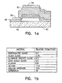
- an FBAR which includes a glass substrate 42, as is illustrated in Fig. 1a .
- the FBAR is formed of similar layers as the FBARs described above, and may be fabricated in accordance with the method of the invention.
- glass to form substrates offers several advantages over the use of semiconductor materials to form substrates.
- One advantage is that glass is inexpensive.
- glass can be used to form chips having large surface areas at an inexpensive cost, thus providing more surface area for bonding.
- Active components such as, by example, transistors and integrated circuits (ICs) can be added onto the chips by, for example, flip-chip technology.
- Fig. 1b illustrates a table showing the respective permittivities of various types of materials.
- soda-lime glass are substantially loss free when being used in microwave frequency applications.
- a further advantage of using glass to form substrates is that, unlike semiconductor materials, most glasses have naturally smooth surfaces. Thus, little or no polishing is required to smooth the surfaces of glass substrates as is required to smooth the surfaces of substrates formed of semiconductor materials.
- thermal expansion characteristics of most types of glass materials are more similar to those of the other materials forming the FBAR layers than are the thermal expansion characteristics of, by example, silicon.
- a component may be encapsulated in glass.
- micromachining glass substrates are not as diverse as those available for micromachining substrates formed of crystalline semiconductor materials.
Landscapes
- Physics & Mathematics (AREA)
- Acoustics & Sound (AREA)
- Engineering & Computer Science (AREA)
- Manufacturing & Machinery (AREA)
- Piezo-Electric Or Mechanical Vibrators, Or Delay Or Filter Circuits (AREA)
Description
- The invention relates to resonators and, in particular, the invention relates to a method for fabricating Thin Film Bulk Acoustic Wave Resonators (FBARs).
- It is known to construct Thin Film Bulk Acoustic Wave Resonators (FBARs) on semiconductor wafers including those which are comprised of Silicon (Si) or gallium arsenide (GaAs). For example, in an article entitled "Acoustic Bulk Wave Composite Resonators", Applied Physics Lett., Vol. 38, No. 3, pp. 125-127, Feb. 1, 1981, by K.M. Lakin and J.S. Wang, an acoustic bulk wave resonator is disclosed which comprises a thin film piezoelectric layer of Zinc-Oxide (ZnO) sputtered over a thin membrane of Silicon (Si).
- Unfortunately, semiconductor materials have high conductivities and high dielectric permittivity characteristics. These characteristics can have a deleterious effect on piezoelectric coupling efficiency and resonator quality factors, as is described in an article entitled "Temperature Compensated High Coupling and High Quality Factor ZnO/SiO2 Bulk Wave Resonators on High Resistance Substrates", IEEE Ultrasonics Symp., 1984, pp. 405-410, by T. Shiosaki, T. Fukuichi, M. Tokuda, and A. Kawabata.
- It is known to reduce ohmic losses exhibited by semiconductor wafers by using semi-insulating semiconductor wafers, as is evidenced by an article entitled "Coplanar Waveguides and Microwave Inductors on Silicon Substrates", IEEE Trans. Microwave Theory Tech., vol. 43, no. 9, pp. 2016-2021, 1995, by Adolfo C. Reyes, Samir M. El-Ghazaly, Steve J. Dorn, Michael Dydyk, Dieter K. Schroder, and Howard Patterson. However, the use of these types of wafers necessitates the use of expensive special grade materials, and does not eliminate the presence of stray capacitances.
- Additionally, semiconductor wafers and crystalline wafers need to be carefully polished after being cut from a crystal in order to smooth their surfaces. The polishing process can be expensive.
- It would be advantageous to provide a substrate that is formed of a low cost material and which exhibits a low permittivity characteristic and low parasitic capacitances. It would also be advantageous to provide a substrate that is formed of a material that does not need to be polished in order to smooth its surfaces.
- It is known to construct so called "bridge" structures on FBAR substrate surfaces using a sacrificial layer that is formed of zinc-oxide (ZnO), as is evidenced by an article entitled "An Air-Gap Type Piezoelectric Composite Thin Film Resonator", IEEE Proc. 39th Annual Symp. Freq. Control, pp. 361-366, 1985, by Hiroaki Satoh, Yasuo Ebata, Hitoshi Suzuki, and Choji Narahara. Similarly, in an article entitled "Multi-layered Ultrasonic Transducers Employing Air-Gap Structure", IEEE Trans. Ultrason. Ferroelec. Freq. Control, vol. 42, no. 3, May 1995, by Susumu Yoshimoto, Masamichi Sakamoto, Ken-ya Hashimoto, and Masatsune Yamaguchi, a multi-layered ultrasonic transducer is disclosed which includes an air gap formed by the removal of a "sacrificial" ZnO layer.
U.S. Pat. No. 4,642,508 to Suzuki et al , entitled "Piezoelectric Resonating Device", also describes a thin film resonator where an air gap between the substrate and a SiO2 film layer that supports a piezoelectric layer is formed by disposing ZnO and dissolving it with a dilute acid to leave the air gap. - During the fabrication of these types of FBARs, a sacrificial layer of ZnO is deposited (e.g., sputtered) over a substrate. The sacrificial layer is later removed via an etching step that is performed after all of the layers of the FBAR have been completely formed. One drawback of this process is that the steps of sputtering and forming the sacrificial layer can be tedious and time-consuming. This is because ZnO is a ceramic material, and thus is brittle and has a low thermal conductivity. If, by example, very high power is employed during the sputtering of the ZnO, the "target" substrate may break. Also, the growth rate of the ZnO must be controlled to produce a correct crystal orientation and crystallite size distribution. Thus, the growth rate may need to be limited to only 2µm/h.
- Another drawback of using a sacrificial layer formed of ZnO is that the surface of the crystalline ZnO film is textured, and thus causes acoustic energy scattering losses to occur within the FBAR. Also, the textured surface of the ZnO may cause the surface of a layer (e.g., the bridge layer) formed over the sacrificial ZnO layer to become deformed. A further drawback of employing a sacrificial layer of ZnO is that during the etching of the layer to form an air gap, a piezoelectric ZnO layer that is formed on the sacrificial layer can become damaged.
- In view of these problems, it can be appreciated that it would be advantageous to provide a method for fabricating an FBAR using a sacrificial layer that is formed of a material having characteristics that are more beneficial than those of ZnO and other materials conventionally used to form sacrificial layers.
- It is a first object of this invention to provide a Thin Film Bulk Acoustic Wave Resonator (FBAR) having a sacrificial layer that is formed of a material that has more beneficial characteristics than conventional materials that are used to form sacrificial layers.
- It is a second object of this invention to provide an improved method for fabricating this Thin Film Bulk Acoustic Wave Resonator (FBAR).
- It is a third object of this invention to provide a Thin Film Bulk Acoustic Wave Resonator (FBAR) having a substrate that is formed of a material that has more beneficial characteristics than conventional materials that are used to form substrates.
- Further objects and advantages of this invention will become apparent from a consideration of the drawings and ensuing description.
- The foregoing and other problems are overcome and the objects of the invention are realized by a method for fabricating a Thin Film Bulk Acoustic Wave Resonator (FBAR). The method of the present invention employs a sacrificial layer that is comprised of either a metal or polymer material instead of a conventionally-used material such as, by example, zinc-oxide (ZnO). The use of these materials to form sacrificial layers has many advantages over the use of ZnO to form these layers.
- In accordance with the method of the invention, a first step includes sputtering a metal such as, by example copper (Cu) over a substrate. The sputtered Cu is then patterned to form a sacrificial layer.
- A next step includes depositing silicon dioxide (SiO2) over the sacrificial layer and over selected portions of the substrate to form a first SiO2 layer (also referred to as a "first protective layer"). This layer may not be needed in cases in which the piezoelectric layer comprises a material which will not be detrimentally affected by the etching of the sacrificial layer (which will be described below). Thereafter, a metallic material such as, by example, gold (Au) is deposited over a selected portion of the first SiO2 layer. The deposited gold is then patterned to form a bottom electrode layer.
- A next step includes depositing zinc-oxide (ZnO) over a selected portion of the bottom electrode layer, and over a selected portion of the first SiO2 layer. The ZnO is then patterned to form a ZnO layer (also referred to as a "piezoelectric layer").
- A next step of the process includes depositing a further metallic material such as, by example, gold, over a selected portion of the ZnO layer. Thereafter, the deposited gold is patterned to form a top electrode layer. In appropriate cases, a second protective layer may also be formed on the structure to protect the piezoelectric layer during the formation of the vias and/or during the etching of the sacrificial layer which will be described below.
- Vias are then formed in the structure so that the sacrificial layer can be removed. Thereafter, the sacrificial layer is removed through the vias to form an air gap.
- The fabrication process of the invention may also be performed using a sacrificial layer that is comprised of a polymer instead of a metal. The steps of this process are similar to those described above, except that the steps of depositing, patterning, and removing the sacrificial layer (e.g., the polymer) are performed in a different manner. By example, the step of depositing the polymer is performed by spinning the polymer onto the substrate. The polymer is then patterned to form the sacrificial layer. After each of the other layers and the vias of the FBAR have been formed in the same manner as described above, the sacrificial layer is removed to form the air gap.
- The type of polymer used to form the sacrificial layer is preferably one that can withstand the high temperatures that can be reached during the sputtering of the ZnO layer.
- In accordance with another aspect of the invention, the method for fabricating FBARs may be performed by removing the sacrificial layer prior to the deposition of the material forming the ZnO layer. For this method, the same steps described above are performed, except that after the first SiO2 layer and the bottom electrode layer have been formed, the sacrificial layer is then removed to form the air gap in the same manner as described above. Thereafter, the steps of forming the ZnO layer and the top electrode layer are carried out in the same manner as described above.
- The use of metals and polymers to form sacrificial layers has many advantages over the use of most conventionally-used materials including, by example, ZnO. For example, FBARs having sacrificial layers that are comprised of metals or polymers can be fabricated more quickly than the FBARs having sacrificial layers formed of ZnO. Also, metals and polymers generally have smoother surfaces than ZnO. Moreover, metals and polymers can be etched using chemicals that are not harmful to piezoelectric layers formed of, by example, ZnO.
- In accordance with a further aspect of the invention, an FBAR is provided which includes a glass substrate. The FBAR is formed of similar layers as the FBARs described above, and may be fabricated in accordance with the method of the invention. The use of glass to form substrates offers several advantages over the use of other materials to form substrates. Glass is inexpensive and thus can be used to form substrates having large surface areas at an inexpensive cost. Also, most glass materials exhibit low permittivity characteristics and low parasitic capacitances. Moreover, most glass materials become substantially loss free when used in microwave frequency applications.
- A further advantage of using glass to form substrates is that, unlike semiconductor materials, glass can have inherently smooth surfaces and thus requires little or no polishing.
- The above set forth and other features of the invention are made more apparent in the ensuing Detailed Description of the Invention when read in conjunction with the attached Drawings, wherein:
-
Fig. 1a illustrates a cross section of an exemplary FBAR having a glass substrate. -
Fig. 1b illustrates a table showing permittivities for various types of materials. -
Fig. 2a illustrates a top view of a portion of an exemplary FBAR having vias. -
Fig. 2b illustrates a cross section of a portion of an exemplary FBAR. -
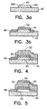
Fig. 3a illustrates a cross section of a portion of a Thin Film Bulk Acoustic Wave Resonator (FBAR) that is formed in accordance with a step of a fabrication process of the invention, for a case in which the portion of the FBAR comprises a sacrificial layer formed of Copper (Cu). -
Fig. 3b illustrates a cross section of the FBARFig. 3a as it appears after a further step of the fabrication process performed in accordance with the invention. -
Fig. 4 illustrates a cross section of the FBAR ofFig. 3b as it appears after a further step of the fabrication process performed in accordance with the invention. -
Fig. 5 illustrates a cross section of the FBAR resonator ofFig. 4 as it appears after a further step of the fabrication process performed in accordance with the invention. -
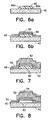
Fig. 6a illustrates a cross section of a portion of Thin Film Bulk Acoustic Wave Resonator (FBAR) that is formed in accordance with a step of the fabrication process of the invention, for a case in which the portion of the FBAR comprises a sacrificial layer formed of a polymer material. -
Fig. 6b illustrates a cross section of the FBARFig. 6a as it appears after a further step of the fabrication process performed in accordance with the invention. -
Fig. 7 illustrates a cross section of the FBAR ofFig. 6b as it appears after a further step of the fabrication process performed in accordance with the invention. -
Fig. 8 illustrates a cross section of the FBAR ofFig. 7 as it appears after a further step of the fabrication process performed in accordance with the invention. -
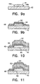
Fig. 9a illustrates a cross section of a portion of a Thin Film Bulk Acoustic Wave Resonator (FBAR) that is formed in accordance with a step of an alternate fabrication process of the invention. -
Fig. 9b illustrates a cross section of the FBARFig. 9a as it appears after a further step of the alternate fabrication process of the invention. -
Fig. 10 illustrates a cross section of the FBAR ofFig. 9b as it appears after a further step of the alternate fabrication process of the invention. -
Fig. 11 illustrates a cross section of the FBAR resonator ofFig. 10 as it appears after a further step of the alternate fabrication process of the invention. - The inventors have developed an improved method for fabricating Thin Film Bulk Acoustic Wave Resonators (FBARs) having air gaps. Unlike most of the conventional methods for fabricating FBARs, which employ sacrificial layers formed of, by example, zinc-oxide (ZnO), the method of the present invention employs a sacrificial layer that is comprised of either a metal or a polymer material. The use of these materials to form sacrificial layers has many advantages over the use of ZnO to form these layers, as will be described below.
- The method of fabricating FBARs in accordance with the invention can be understood in view of
Figs. 3a-5 . As a first step of the fabrication process, a metal such as, by example, copper (Cu) is sputtered or otherwise deposited over asubstrate 42. It is assumed that the substrate is comprised of glass, in accordance with an aspect of this invention which will be further described below, although any other suitable solid material may be employed. The sputtered Cu is then patterned so that it has a thickness of, by example, approximately 2000nm, thereby forming bridges. - Thereafter, the Cu is wet etched to form tapered
edges - It should be noted that other metals may be used in lieu of copper to form the
sacrificial layer 44. By example, thesacrificial layer 44 may be formed of aluminum, zinc, antimony, and any of the elements in the periodic table extending from titanium to copper, from yttrium to silver, and from lanthanum to gold. Ideally, the metals used to form thelayer 44 are low cost and can be etched without great difficulty. - Referring to
Fig. 3b , a next step includes depositing silicon-dioxide (SiO2) over thesacrificial layer 44 and over selected portions of thesubstrate 42 to form a first SiO2 layer (also referred to as a "first protective layer") 48 having a thickness of, by example, approximately 300nm. Thereafter, a metallic material such as, by example, gold (Au) is deposited over a selected portion of the first SiO2 layer 48. The deposited gold is then patterned to form abottom electrode layer 50 having a thickness of, by example, approximately 300 nm. Other suitable electrically conductive metallic and non-metallic materials can also be employed. - It should be noted that for cases in which the material used to form the piezoelectric layer (to be described below) is not detrimentally effected by the etching of the sacrificial layer (the etching of the sacrificial layer will be described below), it is not necessary to employ the first
protective layer 48, and the bottom electrode layer may be formed directly over thesacrificial layer 44 and selected portions of thesubstrate 42. - Referring to
Fig. 4 , a next step includes depositing zinc-oxide (ZnO) over a selected portion of thebottom electrode layer 50, and over a selected portion of the first SiO2 layer 48. The ZnO may be deposited by, for example, sputtering from a target in a mixture of Argon (Ar) and O2. After the ZnO is deposited, it is patterned to form a ZnO layer (also referred to as a "piezoelectric layer") 52 having a selected thickness (e.g., approximately 2000nm) that is a function of a desired resonant frequency of the FBAR. - A next step of the process includes depositing a further metallic material such as, by example, gold, over a selected portion of the
ZnO layer 52. Thereafter, the deposited gold is patterned to form atop electrode layer 54, which is illustrated inFig. 5 . As with thefirst electrode layer 50, other suitable electrically conductive metallic and non-metallic materials can also be employed. - Vias are then formed in the structure so that the
sacrificial layer 44 can be removed. The vias may be formed in any suitable manner. For example, and referring toFig. 2a , selected portions of thefirst SiO2 layer 48 may be removed to provideopenings edges piezoelectric layer 52 during the creation of the vias and/or the removal of the sacrificial layer, a second layer of SiO2 (also referred to as a "second protective layer") (not illustrated inFig. 2a ) may be employed. By example, SiO2 may be deposited and patterned on a selected portion of thepiezoelectric layer 52 after thepiezoelectric layer 52 has been formed and before thetop electrode layer 54 has been formed. The SiO2 is then patterned to form a contact area on a top portion of theZnO layer 52. Within the contact area thetop electrode layer 54 is then formed. In other cases where it is appropriate, the second protective layer may instead be formed after the formation of thetop electrode layer 54 on thepiezoelectric layer 52. - Vias may also be formed in the structure according to the example shown in
Fig. 2b . For this example, holes may be formed in theZnO layer 52 by an using an acid etchant. Selected portions of the FBAR and the surrounding wafer may then be covered by depositing a second protective layer ofSiO 2 51 via, for example, a plasma-enhanced chemical vapor deposition (CVD). The SiO2 is then patterned in fluorine plasma (F plasma) to form a contact area on a top portion of theZnO layer 52. Then, thetop electrode layer 54 is formed over the contact area and over portions of the second layer ofSiO 2 51. Thereafter, selected portions of the second layer ofSiO 2 51 and selected portions of the first SiO2 layer 48 are patterned to form vias (via 49' is shown inFig. 2b ). For this example, it should be noted that as described above with respect toFig. 2a , instead of depositing and patterning the secondprotective layer 51 prior to the formation of thetop electrode layer 54, the secondprotective layer 51 may be deposited and patterned after the formation of thetop electrode layer 54. - A next step of the fabrication process includes removing the
sacrificial layer 44 through the vias by wet etching to form anair gap 62. The etching may be performed by using, for example, acids, alkalis, or redox reactions (e.g., ferric chloride). Either selective or non-selective etching may be used. - In order to determine whether the device is correctly tuned, the electrical performance characteristics of the device can then be measured in a suitable manner and compared with a model of the device. Any suitable technique may be employed for modeling the device including that disclosed in an article entitled "Systematic Design of Stacked-Crystal Filters by Microwave Network Methods", IEEE Trans. Microwave Theory Tech., vol. MTT-22, pp. 14-25, Jan. 1974, by Arthur Ballato, Henry L. Bertoni, and Theodor Tamir.
-
Figs. 6a-8 illustrate steps of the fabrication process of the invention using a sacrificial layer that is formed of a polymer instead of a metal. The steps of this process are similar to those described above, except that the steps of depositing, patterning, and removing the sacrificial layer (e.g., the polymer) are performed in a different manner. Referring toFig. 6a , by example, the step of depositing the polymer is preferably performed by spinning the polymer onto thesubstrate 42 thereby providing an inherently smooth surface for further processing. The polymer is then patterned so that it has a thickness of, by example, approximately 1000nm, thereby forming bridges. The polymer is also etched to form taperededges sacrificial layer 60 is formed. After each of the other layers and the vias of the FBAR have been formed in the same manner as described above (Figs. 6b and 7 ), thesacrificial layer 60 is then removed by, for example, etching or plasma aching. In this manner,air gap 62 is formed, which is illustrated inFig. 8 . - For cases in which organic polymers are used to form the
sacrificial layer 60, thesacrificial layer 60 can be etched in, by example, a plasma containing oxygen. For cases in which silicone polymers are used, for example, an addition of fluorine may be necessary. - Also, some types of polymers can be dissolved in organic solvents (e.g., acetone). Unlike the corrosive chemicals that are used for, by example, anisotropic etching of silicon, organic solvents do not attack ZnO. Thus, polymers which can be dissolved by organic solvents are preferred. Also, the use of this type of bridge structure avoids drawbacks that can be associated with the performance of, by example, deep anisotropic etching of silicon, which requires the etching of a large surface area because the etch stopping crystal plane is angled at, by example, only 54.74 degrees with respect to the surface of the wafer.
- The type of polymer used to form the
sacrificial layer 60 is also preferably one that can withstand the high temperatures that can be reached during the sputtering of theZnO layer 52. The polymer may be, by example, polytetrafluoroethylene or a derivative thereof, polyphenylene sulfide, polyetheretherketone, poly(para phenylene benzobismidazole), poly(para phenylene benzobisoxazole), poly (para phenylene benzobismidazole), poly (para phenylene benzobisthiazole), a polyimide, polyimide siloxane, vinyle ethers, polyphenyl, parylene-n, parylene-f, benzocyclobutene. - In accordance with another aspect of the invention, the method for fabricating FBARs may be performed by removing the sacrificial layer prior to the deposition of the material forming the
ZnO layer 52. This may be understood in view ofFigs. 9a-11 wherein portions of an exemplary FBAR that is formed in accordance with this method of the invention are illustrated. The FBAR includes asacrificial layer 44 formed of, by example, copper (Cu). For this method, the same steps described above are performed, except that after the first SiO2 layer 48, thebottom electrode layer 50, and the vias have been formed, thesacrificial layer 44 is then removed to form theair gap 62 in the same manner as described above. Thereafter, the steps of forming theZnO layer 52 and thetop electrode layer 54 are carried out in the same manner as described above. - The use of metal or polymer materials to form sacrificial layers enables the fabrication process to be performed more quickly than the fabrication processes employing sacrificial layers that are formed of, by example ZnO. This is because ZnO is a brittle ceramic material and thus requires more time to be deposited than metals or polymers which are not as brittle as ZnO.
- The use of polymers or metals to form sacrificial layers also avoids problems that can be associated with the use of most conventionally-used materials (e.g., zinc-oxide) to form such layers. By example, unlike some materials, metals have small grain sizes, and thus have naturally smooth surfaces. Also, polymers can be spun-on during the fabrication of FBAR structures, and develop smooth surfaces during baking while the polymer reflows in a liquid state. As a result, the layer formed over the polymer sacrificial layer does not experience surface deformations that are as serious as those which can occur to layers deposited over most conventionally-used materials (e.g., ZnO).
- Another advantage of using metals or polymers to form sacrificial layers instead of, by example, ZnO is that metals and polymers can be etched using chemicals that are not harmful to the
ZnO layer 52. - In accordance with a further aspect of the invention, an FBAR is provided which includes a
glass substrate 42, as is illustrated inFig. 1a . The FBAR is formed of similar layers as the FBARs described above, and may be fabricated in accordance with the method of the invention. - The use of glass to form substrates offers several advantages over the use of semiconductor materials to form substrates. One advantage is that glass is inexpensive. Thus, glass can be used to form chips having large surface areas at an inexpensive cost, thus providing more surface area for bonding. Active components such as, by example, transistors and integrated circuits (ICs) can be added onto the chips by, for example, flip-chip technology.
- Also, most glass materials including, by example, silicate glass, have low permittivity characteristics, and hence exhibit low parasitic capacitances. Thus, unlike semiconductor materials, which normally have high conductivities and high dielectric permittivity characteristics, glass substrates do not exhibit detrimental characteristics such as, by example, low piezoelectric coupling efficiencies and low resonator quality factors.
Fig. 1b illustrates a table showing the respective permittivities of various types of materials. - In addition, most glass materials except, by example, soda-lime glass, are substantially loss free when being used in microwave frequency applications.
- A further advantage of using glass to form substrates is that, unlike semiconductor materials, most glasses have naturally smooth surfaces. Thus, little or no polishing is required to smooth the surfaces of glass substrates as is required to smooth the surfaces of substrates formed of semiconductor materials.
- Moreover, the thermal expansion characteristics of most types of glass materials are more similar to those of the other materials forming the FBAR layers than are the thermal expansion characteristics of, by example, silicon. As such, in a bonding application, a component may be encapsulated in glass.
- It should be noted that the types of technologies that are available for micromachining glass substrates are not as diverse as those available for micromachining substrates formed of crystalline semiconductor materials.
- While the invention has been particularly shown and described with respect to preferred embodiments thereof, it will be understood by those skilled in the art that changes in form and details may be made therein without departing from the scope of the invention as defined by the following claims.
Claims (21)
- A method for fabricating a thin film bulk acoustic wave resonator, comprising:STEP A: forming a sacrificial layer (44, 60) on a selected portion of a substrate (42);STEP B: forming a bottom electrode layer (50) on the sacrificial layer (44, 60) and on selected portions of the substrate (42);STEP C: forming a piezoelectric layer (52) on a selected portion of the bottom electrode layer (50) and on a selected portion of the substrate (42);STEP D: forming a top electrode layer (54) on a selected portion of the piezoelectric layer (52);STEP E: removing the sacrificial layer (44, 60) to form an air gap (62) beneath at least a portion of the bottom electrode layer (50);characterised in that the sacrificial layer (44, 60) comprises either a metal or a polymer; andwherein STEP A is performed by:depositing either the metal or the polymer over the substrate (42); andpatterning the deposited metal or polymer to form the sacrificial layer (44, 60);wherein between the performances of STEPS D and E, a step is performed of:forming at least one via through at least one of the layers formed in STEPS B-D so that the sacrificial layer (44, 60) can be removed through the at least one via, thereby forming a radio frequency resonator.
- A method as set forth in Claim 1, wherein STEP A is performed by:depositing the metal over the substrate (42); andpatterning the deposited metal to form the sacrificial layer (44, 60).
- A method as set forth in Claim 2, wherein the sacrificial layer (44, 60) is formed of the metal and wherein STEP E is performed by wet-etching the sacrificial layer (44, 60).
- A method as set forth in Claim 1, wherein the metal copper.
- A method as set forth in Claim 1, further comprising depositing a silicone dioxide protective layer (48, 51) having a thickness of 300 nm over the sacrificial layer (44, 60) prior to removing the sacrificial layer (44, 60).
- A method as set forth in Claim 1, wherein the sacrificial layer (44, 60) has a thickness of about 2000 nm.
- A method as set forth in Claim 1, wherein STEP A is performed by:spinning the polymer onto the substrate (42); andpatterning the polymer to form the sacrificial layer (44, 60).
- A method as set forth in Claim 7, wherein the sacrificial layer (44, 60) has a thickness of 1000nm.
- A method as set forth in Claim 1, wherein the substrate (42) comprises silicate glass.
- A method as set forth in Claim 1, wherein the bottom electrode layer (50) comprises an electrically conductive metal having a thickness of 300nm.
- A method as set forth in Claim 1, wherein the piezoelectric layer (52) comprises zinc-oxide having a thickness of 2000nm.
- A method as set forth in Claim 1, wherein the top electrode layer (54) is comprised of an electrically conductive metal having a thickness of 300nm.
- A method as set forth in Claim 1, wherein the substrate (42) is comprised of a solid material.
- A method as set forth in Claim 1, wherein the sacrificial layer (44, 60) is formed of the polymer, and wherein STEP E is performed by one of the steps of etching the sacrificial layer (44, 60) and plasma ashing the sacrificial layer (44, 60).
- A method as set forth in Claim 1, wherein the polymer comprises at least one of a polytetrafluoroethylene, a derivative of polytetrafluoroethylene, polyphenylene sulfide, polyetheretherketone, poly(para phenylene benzobismidazole), poly(para phenylene benzobisoxazole), poly(para phenylene benzobisthiazole), a polyimide, polyimide siloxane, a vinyle ether, polyphenyl, parylen-n, parylene-f, and benzocyclobutene.
- A method as set forth in Claim 1, wherein STEP E is performed between the performances of STEP B and STEP C.
- A method as set forth in Claim 1, wherein the piezoelectric layer (52) comprises zinc-oxide having a thickness that is a function of a desired resonant frequency of the thin film bulk acoustic wave resonator.
- A method as set forth in Claim 1, wherein the substrate (42) is comprised of a glass.
- A method as set forth in Claim 1, comprising disposing an active electrical component to a separate portion of the substrate (42).
- A method as set forth in Claim 19, wherein the active electrical component comprises at least one transistor.
- A method as set forth in claim 19, wherein disposing the active electrical component comprises using a flip-chip technique.
Applications Claiming Priority (3)
| Application Number | Priority Date | Filing Date | Title |
|---|---|---|---|
| US73446796A | 1996-10-17 | 1996-10-17 | |
| US734467 | 1996-10-17 | ||
| PCT/US1997/016231 WO1998016956A1 (en) | 1996-10-17 | 1997-09-12 | Method for fabricating fbars on glass substrates |
Publications (3)
| Publication Number | Publication Date |
|---|---|
| EP1012888A1 EP1012888A1 (en) | 2000-06-28 |
| EP1012888A4 EP1012888A4 (en) | 2001-08-08 |
| EP1012888B1 true EP1012888B1 (en) | 2009-03-04 |
Family
ID=24951811
Family Applications (1)
| Application Number | Title | Priority Date | Filing Date |
|---|---|---|---|
| EP97941066A Expired - Lifetime EP1012888B1 (en) | 1996-10-17 | 1997-09-12 | Method for fabricating fbars on glass substrates |
Country Status (6)
| Country | Link |
|---|---|
| US (1) | US6839946B2 (en) |
| EP (1) | EP1012888B1 (en) |
| JP (1) | JP2002509644A (en) |
| AU (1) | AU4270097A (en) |
| DE (1) | DE69739289D1 (en) |
| WO (1) | WO1998016956A1 (en) |
Families Citing this family (37)
| Publication number | Priority date | Publication date | Assignee | Title |
|---|---|---|---|---|
| US6060818A (en) * | 1998-06-02 | 2000-05-09 | Hewlett-Packard Company | SBAR structures and method of fabrication of SBAR.FBAR film processing techniques for the manufacturing of SBAR/BAR filters |
| US7296329B1 (en) | 2000-02-04 | 2007-11-20 | Agere Systems Inc. | Method of isolation for acoustic resonator device |
| US6662419B2 (en) * | 2001-12-17 | 2003-12-16 | Intel Corporation | Method for fabricating film bulk acoustic resonators to achieve high-Q and low loss |
| JP2004304490A (en) * | 2003-03-31 | 2004-10-28 | Tdk Corp | Method and device for manufacturing thin-film piezoelectric resonator, thin-film piezoelectric resonator, and electronic component |
| KR100489828B1 (en) * | 2003-04-07 | 2005-05-16 | 삼성전기주식회사 | Film bulk acoustic resonator and method of producing the same |
| US6904666B2 (en) * | 2003-07-31 | 2005-06-14 | Andrew Corporation | Method of manufacturing microwave filter components and microwave filter components formed thereby |
| JP4534158B2 (en) | 2003-12-19 | 2010-09-01 | 宇部興産株式会社 | Method for manufacturing piezoelectric thin film device |
| JP3945486B2 (en) | 2004-02-18 | 2007-07-18 | ソニー株式会社 | Thin film bulk acoustic resonator and manufacturing method thereof |
| WO2005104257A1 (en) * | 2004-04-23 | 2005-11-03 | Agency For Science, Technology And Research | Micro-electromechanical device |
| JP4077805B2 (en) | 2004-04-23 | 2008-04-23 | 松下電器産業株式会社 | Manufacturing method of resonator |
| US20060017352A1 (en) * | 2004-07-20 | 2006-01-26 | Aram Tanielian | Thin device and method of fabrication |
| JP2006060385A (en) | 2004-08-18 | 2006-03-02 | Matsushita Electric Ind Co Ltd | Resonator and filter using the same |
| JP2006166419A (en) * | 2004-11-10 | 2006-06-22 | Murata Mfg Co Ltd | Piezoelectric thin film resonator and manufacturing method thereof |
| US20060125577A1 (en) * | 2004-12-13 | 2006-06-15 | International Semiconductor Techonology Ltd. | Acoustic resonator device and method for manufacturing the same |
| JP4379475B2 (en) * | 2004-12-24 | 2009-12-09 | 株式会社村田製作所 | Piezoelectric thin film resonator and manufacturing method thereof |
| WO2006134744A1 (en) * | 2005-06-17 | 2006-12-21 | Murata Manufacturing Co., Ltd. | Electronic component manufacturing method |
| US7486003B1 (en) * | 2005-09-22 | 2009-02-03 | Sei-Joo Jang | Polymer bulk acoustic resonator |
| US7362035B2 (en) * | 2005-09-22 | 2008-04-22 | The Penn State Research Foundation | Polymer bulk acoustic resonator |
| WO2009011022A1 (en) * | 2007-07-13 | 2009-01-22 | Fujitsu Limited | Piezoelectric thin film resonant element and circuit component using the same |
| WO2011036979A1 (en) * | 2009-09-28 | 2011-03-31 | 太陽誘電株式会社 | Acoustic wave device |
| US8692631B2 (en) * | 2009-10-12 | 2014-04-08 | Hao Zhang | Bulk acoustic wave resonator and method of fabricating same |
| US8207453B2 (en) | 2009-12-17 | 2012-06-26 | Intel Corporation | Glass core substrate for integrated circuit devices and methods of making the same |
| US9420707B2 (en) | 2009-12-17 | 2016-08-16 | Intel Corporation | Substrate for integrated circuit devices including multi-layer glass core and methods of making the same |
| WO2011091107A2 (en) * | 2010-01-20 | 2011-07-28 | Arizona Board Of Regents, A Body Corporate Of The State Of Arizona Acting For And On Behalf Of Arizona State University | Film bulk acoustic wave resonator-based ethanol and acetone sensors and methods using the same |
| US8816567B2 (en) | 2011-07-19 | 2014-08-26 | Qualcomm Mems Technologies, Inc. | Piezoelectric laterally vibrating resonator structure geometries for spurious frequency suppression |
| WO2013133827A1 (en) | 2012-03-07 | 2013-09-12 | Intel Corporation | Glass clad microelectronic substrate |
| US9001520B2 (en) | 2012-09-24 | 2015-04-07 | Intel Corporation | Microelectronic structures having laminated or embedded glass routing structures for high density packaging |
| US9615453B2 (en) | 2012-09-26 | 2017-04-04 | Ping-Jung Yang | Method for fabricating glass substrate package |
| US10622310B2 (en) | 2012-09-26 | 2020-04-14 | Ping-Jung Yang | Method for fabricating glass substrate package |
| CN104202010B (en) * | 2014-08-28 | 2017-05-03 | 中国工程物理研究院电子工程研究所 | Hollow cavity-type film bulk acoustic resonator and production method for same |
| RU2617890C2 (en) * | 2014-11-05 | 2017-04-28 | Акционерное общество "Омский научно-исследовательский институт приборостроения" (АО "ОНИИП") | Smoothing method for aluminum film surface on dielectric substrate |
| US10069474B2 (en) * | 2015-11-17 | 2018-09-04 | Qualcomm Incorporated | Encapsulation of acoustic resonator devices |
| US10135415B2 (en) * | 2015-12-18 | 2018-11-20 | Texas Instruments Incorporated | Method to reduce frequency distribution of bulk acoustic wave resonators during manufacturing |
| US11476826B2 (en) | 2017-01-17 | 2022-10-18 | Samsung Electro-Mechanics Co., Ltd. | Bulk acoustic wave resonator |
| US11437977B2 (en) * | 2018-12-14 | 2022-09-06 | Samsung Electro-Mechanics Co., Ltd. | Bulk-acoustic resonator and elastic wave filter device |
| KR102272592B1 (en) * | 2019-01-31 | 2021-07-05 | 삼성전기주식회사 | Bulk-acoustic wave resonator |
| CN111554800B (en) * | 2020-04-23 | 2022-07-26 | 瑞声声学科技(深圳)有限公司 | Planarization method |
Family Cites Families (41)
| Publication number | Priority date | Publication date | Assignee | Title |
|---|---|---|---|---|
| NL277613A (en) | 1961-04-26 | 1900-01-01 | ||
| US3293557A (en) | 1964-03-19 | 1966-12-20 | Bell Telephone Labor Inc | Elastic wave devices utilizing mixed crystals of potassium tantalatepotassium niobate |
| US3422371A (en) | 1967-07-24 | 1969-01-14 | Sanders Associates Inc | Thin film piezoelectric oscillator |
| DE1566009A1 (en) | 1967-08-26 | 1971-02-18 | Telefunken Patent | Mechanical frequency filter and method of its manufacture |
| US3486046A (en) | 1968-10-17 | 1969-12-23 | Westinghouse Electric Corp | Thin film piezoelectric resonator |
| US3696312A (en) | 1970-06-30 | 1972-10-03 | Ibm | Cyclotron resonance devices controllable by electric fields |
| US3686579A (en) | 1971-06-21 | 1972-08-22 | Zenith Radio Corp | Solid-state, acoustic-wave amplifiers |
| US3723920A (en) | 1971-06-24 | 1973-03-27 | Gte Automatic Electric Lab Inc | Crystal filter assembly |
| FR2151727A5 (en) | 1971-09-10 | 1973-04-20 | Thomson Csf | |
| FR2182295A5 (en) | 1972-04-25 | 1973-12-07 | Thomson Csf | |
| SE384958B (en) | 1974-07-19 | 1976-05-24 | Philips Svenska Ab | KIT FOR TRANSMISSION OF INFORMATION IN A TRANSPONDER SYSTEM AND DEVICE FOR PERFORMING THE KIT |
| AT353506B (en) | 1976-10-19 | 1979-11-26 | List Hans | PIEZOELECTRIC RESONATOR |
| GB1592010A (en) | 1977-01-12 | 1981-07-01 | Suwa Seikosha Kk | Contour vibrator |
| CH630747A5 (en) | 1979-01-18 | 1982-06-30 | Ebauches Sa | METHOD FOR ADJUSTING THE FREQUENCY OF A RESONATOR AND RESONATOR WITH ADJUSTED FREQUENCY OBTAINED BY THE IMPLEMENTATION OF THIS PROCESS. |
| JPS56100510A (en) | 1980-01-16 | 1981-08-12 | Clarion Co Ltd | Elastic surface wave device |
| US4320365A (en) | 1980-11-03 | 1982-03-16 | United Technologies Corporation | Fundamental, longitudinal, thickness mode bulk wave resonator |
| JPS58137317A (en) | 1982-02-09 | 1983-08-15 | Nec Corp | Thin-film piezoelectric compound oscillator |
| CH661587A5 (en) * | 1983-03-29 | 1987-07-31 | Loepfe Ag Geb | LENGTH MEASURING DEVICE FOR A THREAD ON A THREAD WINDING DEVICE. |
| US4502932A (en) | 1983-10-13 | 1985-03-05 | The United States Of America As Represented By The United States Department Of Energy | Acoustic resonator and method of making same |
| US4556812A (en) | 1983-10-13 | 1985-12-03 | The United States Of America As Represented By The United States Department Of Energy | Acoustic resonator with Al electrodes on an AlN layer and using a GaAs substrate |
| JPS60189307A (en) * | 1984-03-09 | 1985-09-26 | Toshiba Corp | Piezoelectric thin film resonator and its manufacture |
| JPS6276913A (en) | 1985-09-30 | 1987-04-09 | Toshiba Corp | Thin film elastic wave device |
| US4897618A (en) | 1989-06-05 | 1990-01-30 | The Curran Company | Harmonic frequency selecting circuit |
| US5162691A (en) * | 1991-01-22 | 1992-11-10 | The United States Of America As Represented By The Secretary Of The Army | Cantilevered air-gap type thin film piezoelectric resonator |
| US5233259A (en) | 1991-02-19 | 1993-08-03 | Westinghouse Electric Corp. | Lateral field FBAR |
| US5153476A (en) | 1991-03-11 | 1992-10-06 | The United States Of America As Represented By The Secretary Of The Army | Acoustic vibrator with variable sensitivity to external acceleration |
| US5185589A (en) | 1991-05-17 | 1993-02-09 | Westinghouse Electric Corp. | Microwave film bulk acoustic resonator and manifolded filter bank |
| US5166646A (en) | 1992-02-07 | 1992-11-24 | Motorola, Inc. | Integrated tunable resonators for use in oscillators and filters |
| US5382930A (en) | 1992-12-21 | 1995-01-17 | Trw Inc. | Monolithic multipole filters made of thin film stacked crystal filters |
| US5373268A (en) | 1993-02-01 | 1994-12-13 | Motorola, Inc. | Thin film resonator having stacked acoustic reflecting impedance matching layers and method |
| US5619061A (en) * | 1993-07-27 | 1997-04-08 | Texas Instruments Incorporated | Micromechanical microwave switching |
| US5332943A (en) | 1993-10-21 | 1994-07-26 | Bhardwaj Mahesh C | High temperature ultrasonic transducer device |
| US5446306A (en) | 1993-12-13 | 1995-08-29 | Trw Inc. | Thin film voltage-tuned semiconductor bulk acoustic resonator (SBAR) |
| US5587620A (en) | 1993-12-21 | 1996-12-24 | Hewlett-Packard Company | Tunable thin film acoustic resonators and method for making the same |
| US5422533A (en) | 1994-03-09 | 1995-06-06 | The United States Of America As Represented By The Secretary Of The Army | Piezoelectric resonator |
| US5629906A (en) | 1995-02-15 | 1997-05-13 | Hewlett-Packard Company | Ultrasonic transducer |
| US5596239A (en) * | 1995-06-29 | 1997-01-21 | Motorola, Inc. | Enhanced quality factor resonator |
| US5692279A (en) | 1995-08-17 | 1997-12-02 | Motorola | Method of making a monolithic thin film resonator lattice filter |
| CN1110132C (en) * | 1995-09-21 | 2003-05-28 | Tdk株式会社 | Surface acoustic wave device and manufacturing method thereof |
| US5646583A (en) | 1996-01-04 | 1997-07-08 | Rockwell International Corporation | Acoustic isolator having a high impedance layer of hafnium oxide |
| US5714917A (en) * | 1996-10-02 | 1998-02-03 | Nokia Mobile Phones Limited | Device incorporating a tunable thin film bulk acoustic resonator for performing amplitude and phase modulation |
-
1997
- 1997-09-12 DE DE69739289T patent/DE69739289D1/en not_active Expired - Lifetime
- 1997-09-12 WO PCT/US1997/016231 patent/WO1998016956A1/en not_active Ceased
- 1997-09-12 AU AU42700/97A patent/AU4270097A/en not_active Abandoned
- 1997-09-12 EP EP97941066A patent/EP1012888B1/en not_active Expired - Lifetime
- 1997-09-12 JP JP51834498A patent/JP2002509644A/en active Pending
-
2002
- 2002-10-22 US US10/278,612 patent/US6839946B2/en not_active Expired - Lifetime
Non-Patent Citations (1)
| Title |
|---|
| YOSHIMOTO S. ET AL: "MULTI-LAYERED ULTRASONIC TRANSDUCERS EMPLOYING AIR-GAP STRUCTURE", IEEE TRANSACTIONS ON ULTRASONICS, FERROELECTRICS AND FREQUENCY CONTROL,, vol. 42, no. 3, 1 May 1995 (1995-05-01) - 1 May 1995 (1995-05-01), IEEE SERVICE CENTER, PISCATAWAY, NJ, US, pages 339 - 343, XP000511366 * |
Also Published As
| Publication number | Publication date |
|---|---|
| US6839946B2 (en) | 2005-01-11 |
| AU4270097A (en) | 1998-05-11 |
| DE69739289D1 (en) | 2009-04-16 |
| US20030102773A1 (en) | 2003-06-05 |
| EP1012888A1 (en) | 2000-06-28 |
| JP2002509644A (en) | 2002-03-26 |
| EP1012888A4 (en) | 2001-08-08 |
| WO1998016956A1 (en) | 1998-04-23 |
Similar Documents
| Publication | Publication Date | Title |
|---|---|---|
| EP1012888B1 (en) | Method for fabricating fbars on glass substrates | |
| EP1299946B1 (en) | Filter and method for manufacturing the same | |
| US5873154A (en) | Method for fabricating a resonator having an acoustic mirror | |
| JP4756461B2 (en) | Aluminum nitride thin film and piezoelectric thin film resonator using the same | |
| US7802349B2 (en) | Manufacturing process for thin film bulk acoustic resonator (FBAR) filters | |
| US5894647A (en) | Method for fabricating piezoelectric resonators and product | |
| EP1701440A1 (en) | Method for manufacturing piezoelectric thin-film device and piezoelectric thin-film device | |
| US20030141946A1 (en) | Film bulk acoustic resonator (FBAR) and the method of making the same | |
| US20050231305A1 (en) | Tapered electrode in an acoustic resonator | |
| US20070115078A1 (en) | Film bulk acoustic-wave resonator and method for manufacturing the same | |
| US6675450B1 (en) | Method of manufacturing and mounting electronic devices to limit the effects of parasitics | |
| US8431031B2 (en) | Method for producing a bulk wave acoustic resonator of FBAR type | |
| US12155368B2 (en) | Support structure for bulk acoustic wave resonator | |
| US8522411B1 (en) | Method to control BAW resonator top electrode edge during patterning | |
| JP2007036829A (en) | Thin film piezoelectric resonator, filter, and method of manufacturing thin film piezoelectric resonator | |
| US6657517B2 (en) | Multi-frequency thin film resonators | |
| US8225472B2 (en) | Methods of fabricating a membrane with improved mechanical integrity | |
| JP2001177365A (en) | Adjustment method of center frequency of balanced filter and multiple balanced filters | |
| KR100697398B1 (en) | Piezoelectric Filter Manufacturing Method | |
| Seabury et al. | Thin film ZnO based bulk acoustic mode filters | |
| EP1175727B1 (en) | Method of manufacturing a hybrid integrated circuit comprising a semiconductor element and a piezoelectric filter | |
| KR100480030B1 (en) | Manufacturing method of thin film bulk acoustic resonator and filter |
Legal Events
| Date | Code | Title | Description |
|---|---|---|---|
| PUAI | Public reference made under article 153(3) epc to a published international application that has entered the european phase |
Free format text: ORIGINAL CODE: 0009012 |
|
| 17P | Request for examination filed |
Effective date: 19990517 |
|
| AK | Designated contracting states |
Kind code of ref document: A1 Designated state(s): DE FR GB IT |
|
| A4 | Supplementary search report drawn up and despatched |
Effective date: 20010622 |
|
| AK | Designated contracting states |
Kind code of ref document: A4 Designated state(s): DE FR GB IT |
|
| RIC1 | Information provided on ipc code assigned before grant |
Free format text: 7H 01L 41/08 A, 7H 03H 9/17 B, 7H 03H 3/02 B |
|
| RAP1 | Party data changed (applicant data changed or rights of an application transferred) |
Owner name: NOKIA CORPORATION |
|
| 17Q | First examination report despatched |
Effective date: 20060202 |
|
| GRAP | Despatch of communication of intention to grant a patent |
Free format text: ORIGINAL CODE: EPIDOSNIGR1 |
|
| GRAS | Grant fee paid |
Free format text: ORIGINAL CODE: EPIDOSNIGR3 |
|
| RAP1 | Party data changed (applicant data changed or rights of an application transferred) |
Owner name: AVAGO TECHNOLOGIES WIRELESS IP (SINGAPORE) PTE. LT |
|
| GRAA | (expected) grant |
Free format text: ORIGINAL CODE: 0009210 |
|
| AK | Designated contracting states |
Kind code of ref document: B1 Designated state(s): DE FR GB IT |
|
| REG | Reference to a national code |
Ref country code: GB Ref legal event code: FG4D |
|
| REF | Corresponds to: |
Ref document number: 69739289 Country of ref document: DE Date of ref document: 20090416 Kind code of ref document: P |
|
| PLBE | No opposition filed within time limit |
Free format text: ORIGINAL CODE: 0009261 |
|
| STAA | Information on the status of an ep patent application or granted ep patent |
Free format text: STATUS: NO OPPOSITION FILED WITHIN TIME LIMIT |
|
| 26N | No opposition filed |
Effective date: 20091207 |
|
| REG | Reference to a national code |
Ref country code: FR Ref legal event code: ST Effective date: 20100531 |
|
| PG25 | Lapsed in a contracting state [announced via postgrant information from national office to epo] |
Ref country code: FR Free format text: LAPSE BECAUSE OF NON-PAYMENT OF DUE FEES Effective date: 20090930 |
|
| PG25 | Lapsed in a contracting state [announced via postgrant information from national office to epo] |
Ref country code: IT Free format text: LAPSE BECAUSE OF FAILURE TO SUBMIT A TRANSLATION OF THE DESCRIPTION OR TO PAY THE FEE WITHIN THE PRESCRIBED TIME-LIMIT Effective date: 20090304 |
|
| PGFP | Annual fee paid to national office [announced via postgrant information from national office to epo] |
Ref country code: GB Payment date: 20120912 Year of fee payment: 16 |
|
| REG | Reference to a national code |
Ref country code: DE Ref legal event code: R082 Ref document number: 69739289 Country of ref document: DE Representative=s name: DILG HAEUSLER SCHINDELMANN PATENTANWALTSGESELL, DE Effective date: 20130529 Ref country code: DE Ref legal event code: R081 Ref document number: 69739289 Country of ref document: DE Owner name: AVAGO TECHNOLOGIES GENERAL IP (SINGAPORE) PTE., SG Free format text: FORMER OWNER: AVAGO TECHNOLOGIES WIRELESS IP (SINGAPORE) PTE. LTD., SINGAPORE, SG Effective date: 20130529 |
|
| REG | Reference to a national code |
Ref country code: GB Ref legal event code: 732E Free format text: REGISTERED BETWEEN 20130725 AND 20130731 |
|
| GBPC | Gb: european patent ceased through non-payment of renewal fee |
Effective date: 20130912 |
|
| PG25 | Lapsed in a contracting state [announced via postgrant information from national office to epo] |
Ref country code: GB Free format text: LAPSE BECAUSE OF NON-PAYMENT OF DUE FEES Effective date: 20130912 |
|
| PGFP | Annual fee paid to national office [announced via postgrant information from national office to epo] |
Ref country code: DE Payment date: 20160823 Year of fee payment: 20 |
|
| REG | Reference to a national code |
Ref country code: DE Ref legal event code: R071 Ref document number: 69739289 Country of ref document: DE |