EP1011040B1 - Transparent conductive film for transparent touch panel, transparent touch panel using transparent conductive film, and method of manufacturing transparent conductive film - Google Patents
Transparent conductive film for transparent touch panel, transparent touch panel using transparent conductive film, and method of manufacturing transparent conductive film Download PDFInfo
- Publication number
- EP1011040B1 EP1011040B1 EP99926963A EP99926963A EP1011040B1 EP 1011040 B1 EP1011040 B1 EP 1011040B1 EP 99926963 A EP99926963 A EP 99926963A EP 99926963 A EP99926963 A EP 99926963A EP 1011040 B1 EP1011040 B1 EP 1011040B1
- Authority
- EP
- European Patent Office
- Prior art keywords
- transparent conductive
- conductive film
- film
- touch panel
- transparent
- Prior art date
- Legal status (The legal status is an assumption and is not a legal conclusion. Google has not performed a legal analysis and makes no representation as to the accuracy of the status listed.)
- Expired - Lifetime
Links
Images


Classifications
-
- G—PHYSICS
- G06—COMPUTING; CALCULATING OR COUNTING
- G06F—ELECTRIC DIGITAL DATA PROCESSING
- G06F3/00—Input arrangements for transferring data to be processed into a form capable of being handled by the computer; Output arrangements for transferring data from processing unit to output unit, e.g. interface arrangements
- G06F3/01—Input arrangements or combined input and output arrangements for interaction between user and computer
- G06F3/03—Arrangements for converting the position or the displacement of a member into a coded form
- G06F3/041—Digitisers, e.g. for touch screens or touch pads, characterised by the transducing means
- G06F3/045—Digitisers, e.g. for touch screens or touch pads, characterised by the transducing means using resistive elements, e.g. a single continuous surface or two parallel surfaces put in contact
-
- C—CHEMISTRY; METALLURGY
- C01—INORGANIC CHEMISTRY
- C01G—COMPOUNDS CONTAINING METALS NOT COVERED BY SUBCLASSES C01D OR C01F
- C01G19/00—Compounds of tin
- C01G19/006—Compounds containing, besides tin, two or more other elements, with the exception of oxygen or hydrogen
-
- H—ELECTRICITY
- H01—ELECTRIC ELEMENTS
- H01B—CABLES; CONDUCTORS; INSULATORS; SELECTION OF MATERIALS FOR THEIR CONDUCTIVE, INSULATING OR DIELECTRIC PROPERTIES
- H01B1/00—Conductors or conductive bodies characterised by the conductive materials; Selection of materials as conductors
- H01B1/06—Conductors or conductive bodies characterised by the conductive materials; Selection of materials as conductors mainly consisting of other non-metallic substances
- H01B1/08—Conductors or conductive bodies characterised by the conductive materials; Selection of materials as conductors mainly consisting of other non-metallic substances oxides
-
- C—CHEMISTRY; METALLURGY
- C09—DYES; PAINTS; POLISHES; NATURAL RESINS; ADHESIVES; COMPOSITIONS NOT OTHERWISE PROVIDED FOR; APPLICATIONS OF MATERIALS NOT OTHERWISE PROVIDED FOR
- C09K—MATERIALS FOR MISCELLANEOUS APPLICATIONS, NOT PROVIDED FOR ELSEWHERE
- C09K2323/00—Functional layers of liquid crystal optical display excluding electroactive liquid crystal layer characterised by chemical composition
- C09K2323/04—Charge transferring layer characterised by chemical composition, i.e. conductive
-
- Y—GENERAL TAGGING OF NEW TECHNOLOGICAL DEVELOPMENTS; GENERAL TAGGING OF CROSS-SECTIONAL TECHNOLOGIES SPANNING OVER SEVERAL SECTIONS OF THE IPC; TECHNICAL SUBJECTS COVERED BY FORMER USPC CROSS-REFERENCE ART COLLECTIONS [XRACs] AND DIGESTS
- Y10—TECHNICAL SUBJECTS COVERED BY FORMER USPC
- Y10T—TECHNICAL SUBJECTS COVERED BY FORMER US CLASSIFICATION
- Y10T428/00—Stock material or miscellaneous articles
- Y10T428/24—Structurally defined web or sheet [e.g., overall dimension, etc.]
- Y10T428/24355—Continuous and nonuniform or irregular surface on layer or component [e.g., roofing, etc.]
Definitions
- the present invention relates to a transparent conductive film for use in a transparent touch panel capable of performing stable, light touch inputs, to a transparent touch panel using the transparent conductive film, and to a method for fabricating a transparent conductive film.
- the transparent conductive film for use in a transparent touch panel, the transparent touch panel using the transparent conductive film, and the method for fabricating a transparent conductive film, according to the present invention are particularly suitable as a transparent conductive film for use in a transparent touch panel to be used as an input device by being laminated on a display screen of a flat display such as liquid crystal display devices, electroluminescent elements, plasma display devices, fluorescent character display tables, and field emission displays, and as a transparent touch panel using the transparent conductive film, and as a method for fabricating a transparent conductive film.
- the transparent conductive film to be used as an electrode in a transparent touch panel is generally made of a metallic oxide such as ATO (antimony oxide/tin oxide), FTO (tin oxide/fluorine dope), ITO (indium oxide/tin oxide), FATO (antimony oxide/tin oxide/fluorine dope), or the like.
- ATO antimony oxide/tin oxide
- FTO tin oxide/fluorine dope
- ITO indium oxide/tin oxide
- FATO antimony oxide/tin oxide/fluorine dope
- the resistor-film analog type transparent touch panel is required to have a surface resistance of 200 - 2000 ⁇ /sq and be highly transparent and less colored.
- the resistor-film analog type transparent touch panel has such a structure that a lower electrode substrate comprising an insulating substrate such as a glass plate or a film having on its surface a lower electrode made of a transparent conductive film and dot-like spacers, and an upper electrode substrate comprising an insulating substrate such as a film having on its surface an upper electrode made of a transparent conductive film are laminated.
- the transparent touch panel is thus enabled to make an input by pressing a portion of the surface of the transparent touch panel from the input surface side so that the two electrodes are put into contact and electrically conducting with each other.
- the transparent conductive film formed in the transparent touch panel is normally formed by a physical film formation process such as evaporation process and sputtering process or a chemical vapor phase process such as CVD process.
- JP 09 305313 A shows such a process.
- the mean crystal grain size (R) within a plane observed at the film surface of the transparent conductive film is controllable.
- the mainstream is transparent conductive films made of ITO, where the surface resistance value is required to be 200 - 2000 ⁇ /sq, rather higher as compared with electrodes for liquid crystal displays.
- ITO is low in specific resistance, it is necessary to increase the surface resistance value by forming an ultrathin film having a film thickness of about 100 - 200 ⁇ .
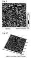
- the mean crystal grain size (R) is as fine as 10 - 15 nm, where the arithmetic mean roughness (Ra) as observed by an atomic force microscope is as small as 0.1 - 0.3 nm and the root-mean-square roughness (Rms) is as small as 0.25 nm.
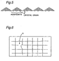
- a surface cross-section of a transparent conductive film is formed generally triangular of grains as shown in Fig. 5 and Figs. 17 to 19 .
- the threshold voltage Evs (see Fig. 7 ) that conditions ON/OFF state upon an input by the transparent touch panel is set low, thereby compensating a voltage reduction due to contact resistance developed between opposing electrodes for an easier input.
- this would make it likely to occur that even unstable inputs are accepted so that coordinate jumps would frequently occur, as an issue. That is, as shown in Fig. 7 , in the case where the threshold voltage Evs is set to a low one as a countermeasure for the phenomenon that the detected voltage Ev (see Fig.
- the contact resistance value Eb fluctuates up and down due to variations in the contact resistance value Eb, for example, where the threshold voltage is set to 3.6 V, if there have been two-place inputs of 4.0 V and 3.5 V simultaneously, such as upon a film contact due to improper strain or upon a finger-and-pen simultaneous contact where a finger contacts a portion near a pen-contact portion at the same time as the pen contacts there, it is decided as a mis-input so that no display is given on the liquid crystal display screen or the like, where a case that there are no coordinate inputs at the relevant portion, i.e., line breaks result (see Fig. 6 ).
- an object of the present invention is to provide a transparent conductive film for use in a transparent touch panel capable of performing stable, light touch inputs, a transparent touch panel using the transparent conductive film, and a method for fabricating a transparent conductive film, by which the above-described issues can be solved.
- Fig. 1 is a schematic sectional view showing a cross-sectional shape of the surface of a transparent conductive film of a transparent touch panel according to an embodiment of the invention.
- Fig. 2 is an atomic force microscope photograph showing crystal grain size of a metallic oxide of the transparent conductive film of the transparent touch panel of the above embodiment of the invention.
- Fig. 3 is a perspective view showing a method for observing voltage drop due to contact resistance between the transparent conductive films of the transparent touch panel of the above embodiment.
- Fig. 4 is a circuit diagram showing a method for observing voltage drop due to contact resistance between the transparent conductive films of the transparent touch panel of the above embodiment.
- Fig. 8 is a schematic view in which an ideal input voltage Ev detected upon an input on the transparent touch panel of the above embodiment is recorded.
- Fig. 9 is a graph for explaining the arithmetic mean roughness of a surface roughness parameter in the transparent touch panel of the above embodiment.
- Fig. 10 is a graph for explaining the center line (average line) depth of a surface roughness parameter in the transparent touch panel of the above embodiment.
- Fig. 11 is a schematic sectional view showing a cross-sectional shape of the surface of the transparent conductive film in the state that the upper electrode and the lower electrode of the transparent touch panel of the above embodiment are opposed to each other.
- Fig. 12 is a schematic sectional view showing a cross-sectional shape of the surface of the transparent conductive film in the state of a pen input performed while the upper electrode and the lower electrode of the transparent touch panel of the above embodiment are opposed to each other.
- FIG. 13 is an atomic force microscope photograph showing crystal grain size of a metallic oxide of the transparent conductive film of the transparent touch panel of the above embodiment of Fig. 2 .
- Fig. 14 is another atomic force microscope photograph showing crystal grain size of a metallic oxide of the transparent conductive film of the transparent touch panel of the above embodiment of the invention.
- Fig. 15 is a graph showing heightwise variations in the crystal grain size of a metallic oxide of the transparent conductive film in a cross section taken along the line A - B of Fig. 14 .
- the positions of A1, A2, A3, A4, A5, A6 in Fig. 15 correspond to the positions of A1, A2, A3, A4, A5, A6 in Fig. 14 , respectively.
- FIG. 16 is a graph showing heightwise variations in the crystal grain size of a metallic oxide of the transparent conductive film in a cross section taken along the line C - D of Fig. 14 .
- the positions of C1, C2, C3, C4, C5, C6 in Fig. 16 correspond to the positions of C1, C2, C3, C4, C5, C6 in Fig. 14 , respectively.
- reference numeral 1 denotes a transparent conductive film
- 2 denotes an input pen
- 3 denotes a bus bar
- 4 denotes an upper electrode
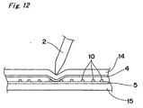
- 5 denotes a lower electrode. Therefore, as shown in Figs. 3 and 12 , input work is performed by pressing a portion of the surface of the transparent touch panel from the input surface side, for example, from the upper electrode 4 side, with the input pen 2 so that the two electrodes 4, 5 both formed of the transparent conductive film 1 are put into contact and electrically conducting with each other, by which input information is transferred to specified equipment via the bus bar 3.
- the lower electrode 5 formed of the transparent conductive film 1 provided on the surface of a lower electrode substrate 15, and the upper electrode 4 formed of the transparent conductive film 1 provided on the surface of an upper electrode substrate 14 are stacked so as to be spaced from each other by a multiplicity of spacers 10 as shown in Figs. 1 , 11 , and 12 .
- the spacers 10 used are, for example, those having a diameter of 20 - 100 ⁇ m, a height of 4 - 25 ⁇ m, and each interval between the spacers 10 of 1 - 5 mm.
- the spacers are normally formed on the surface of either the upper electrode or the lower electrode.
- Substrates as the lower electrode substrate and the upper electrode substrate in this embodiment are exemplified by plastic substrates or glass substrates having thermal resistance and superior in transparency.
- plastic substrates or glass substrates having thermal resistance and superior in transparency.
- the plastic substrates used are polycarbonate resin, polyethylene terephthalate resin, polyethersulfone resin, polyacrylate resin, triacetate resin, or the like.
- the glass substrates have only to be low in hue and not particularly limited.
- the transparent conductive film 1 of this embodiment may be made of a metallic oxide, which is an n-type semiconductor, typified by ATO (antimony oxide/tin oxide), FTO (tin oxide/fluorine dope), ITO (indium oxide/tin oxide), FATO (antimony oxide/tin oxide/fluorine dope), and the like.
- ATO antimony oxide/tin oxide
- FTO tin oxide/fluorine dope
- ITO indium oxide/tin oxide
- FATO antimony oxide/tin oxide/fluorine dope
- the transparent conductive film 1 is so formed that the arithmetic mean roughness (Ra) of the surface shape is within a range of 0.4 nm ⁇ Ra ⁇ 4.0 nm and the root-mean-square roughness (Rms) of the surface shape is within a range of 0.6 nm ⁇ Rms ⁇ 3.0 nm.
- the reason of this is that forming the transparent conductive film 1 like this makes it possible to obtain a film in which crystal grain aggregates are arranged compact as shown in Fig. 1 and yet which has a good smoothness so that a contact area for input operation can promptly be ensured as shown in Figs. 11 and 12 .
- arithmetic mean roughness (Ra) is less than 0.4 nm or if the root-mean-square roughness (Rms) is less than 0.6 nm, a considerably dot-like contact results, which is unsuitable for input operation because of less contact area (see Fig. 5 and Figs. 17 to 19 ). Also, even if either one of the arithmetic mean roughness (Ra) and the root-mean-square roughness (Rms) is within the foregoing range, proper inputs could not be expected.
- the cross section of grain aggregates forming the surface shape is formed into a trapezoidal or rectangular shape as shown in Fig. 1 by setting the following parameter (Rp/Rmax) which represents the surface shape of the transparent conductive film 1 to 0.55 or less (see Figs. 15 and 16 ).
- Rp/Rmax represents the surface shape of the transparent conductive film 1 to 0.55 or less
- the transparent conductive film 1 forming at least one of the electrodes is an indium oxide - tin oxide film
- the cross section of grain aggregates forming the surface shape is formed into a trapezoidal or rectangular shape as shown in Fig.
- the mean crystal grain size (R) within the plane of the metallic oxide observed at the surface of the film is within a range of 40 nm ⁇ R ⁇ 200 nm
- the arithmetic mean roughness (Ra) of the surface of the transparent conductive film 1 is within a range of 0.4 nm ⁇ Ra ⁇ 3.0 nm
- the root-mean-square roughness (Rms) is within a range of 0.6 nm ⁇ Rms ⁇ 2.0 nm
- the parameter (Rp/Rmax) representing the surface shape is 0.55 or less. That is, it is set that Rp/Rmax ⁇ 0.55, where Rp represents the center line depth and Rmax represents the maximum roughness of the surface, both expressed in nm.
- the center line depth Rp and the maximum roughness Rmax will be described later.
- the reason that the mean crystal grain size (R) within the plane of the metallic oxide observed at the surface of the film is set so as to be distributed within the range of 40 nm ⁇ R ⁇ 200 nm is as follows. That is, if the mean crystal grain size (R) is distributed within a range less than 40 nm, then a light touch input would result in an unstable input; if the mean crystal grain size (R) is distributed within a range over 200 nm, then it is extremely difficult to fabricate a transparent conductive film 1 having such a mean crystal grain size (R).
- the mean crystal grain size (R) to within the range of 40 nm ⁇ R ⁇ 200 nm so that a stable oxide film less in barriers typified by grain boundaries is obtained, the contact resistance upon mutual contact of the transparent conductive films provided on opposing substrates can be reduced so that a stable input can be achieved.
- sputtering process is the mainstream for forming the indium oxide - tin oxide film and is capable of obtaining a film of good crystallinity, where such measures as holding the substrate temperature during film formation at high temperatures or performing annealing process at specified temperatures after the film formation are taken for achieving grain growth.
- the growth of crystal grains may be accelerated, for example, by setting the substrate temperature during the film formation to 350°C or by performing an aging process at 150 - 200°C for several hours or more after the film formation.
- coating process and printing process are not only simpler in engineering technique but also easier in grain control as well as easier in adjustment of specific resistance, than sputtering process. Furthermore, coating process and printing process are suitable for controlling the surface shape.
- the arithmetic mean roughness (Ra) is 0.21 nm and the root-mean-square roughness (Rms) is 0.26 nm in the A - B line portion and 0.28 nm in the C - D line portion.
- the vertical axis represents height and the horizontal axis represents distance.
- the mean crystal grain size (R) within the plane observed at the surface of the transparent conductive film is as fine as 10 - 15 nm
- an increase in surface resistance value occurs upon the foregoing humidity heat test, and a considerable increase in occurrence of mis-inputs occurs with light touch inputs.
- the reason of this could be considered that with a small mean crystal grain size (R), the surface area of the transparent conductive film increases and so the amount of moisture adsorption is large, causing carriers in the transparent conductive film to be removed, with the result that the surface resistance value is increased.
- the cross section of grain aggregates forming the surface shape is formed into a trapezoidal or rectangular shape as shown in Fig.
- the mean crystal grain size (R) within the plane of the metallic oxide observed at the surface of the film is within a range of 80 nm ⁇ R ⁇ 400 nm
- the arithmetic mean roughness (Ra) of the surface of the transparent conductive film 1 is within a range of 0.4 nm ⁇ Ra ⁇ 4.0 nm
- the root-mean-square roughness (Rms) is within a range of 0.6 nm ⁇ Rms ⁇ 3.0 nm
- the parameter (Rp/Rmax) representing the surface shape is 0.55 or less. That is, it is set that Rp/Rmax ⁇ 0.55, where Rp represents the center line depth and Rmax represents the maximum roughness, both expressed in nm.
- the center line depth Rp and the maximum roughness Rmax will be described later.
- the reason that the mean crystal grain size (R) within the plane of the metallic oxide observed at the surface of the film is set so as to be distributed within the range of 80 nm ⁇ R ⁇ 400 nm is as follows. That is, if the mean crystal grain size (R) is distributed within a range less than 80 nm, then a light touch input would result in an unstable input; if the mean crystal grain size (R) is distributed within a range over 400 nm, then the transparent conductive film serving as the opposing electrode would be damaged by surface irregularities, thus the transparent conductive film 1 being inferior in sliding durability.
- the mean crystal grain size (R) to within the range of 80 nm ⁇ R ⁇ 400 nm so that a crystal-grown, stable oxide film is obtained, the contact resistance upon mutual contact of the transparent conductive films provided on opposing substrates can be reduced so that a stable input can be achieved.
- vapor phase methods typified by CVD process is the mainstream for forming the fluorine- or antimony-added tin oxide film.
- the film formation temperature is as high as 450°C - 550°C and therefore the growth of crystal grains can be controlled so that the mean crystal grain size (R) is set within the range of 80 nm ⁇ R ⁇ 400 nm.
- the size of the crystal grains can be controlled so as to fall within the aforementioned range by adjusting the addition amount or dispersibility of various kinds of elements in solution state as well as the free energy of ink and further by taking into consideration drying process and burning conditions.
- This thin film formation apparatus is constructed by: an intaglio roll 103 rotatably supported on a support frame of a base and having a multiplicity of 1.0 - several 10 ⁇ m deep ink cells on its surface; an ink feeder unit 105 for feeding 1.0 - 30,000 mPas ink to the surface of the intaglio roll 103; a doctor 106 which is provided at a specified site around the intaglio roll 103 supported on the support frame 102 and which makes a constant amount of ink held within the ink cells by spreading the ink, which has been fed to the intaglio roll 103, over the intaglio roll surface; a print roll 104 which is rotatably supported on the support frame 102 below the intaglio roll 103 and which has a
- the mean crystal grain size (R) within the foregoing range can be easily obtained, and it is easy to control the arithmetic mean roughness (Ra) and the root-mean-square roughness (Rms) to within the foregoing ranges.
- the constituent weight ratio of indium to tin is less than 5 wt%, the amount of tin added as a dopant is so low that the generation of carriers serving for electrical conduction could not be expected. That is, the specific resistance of the film would be 1.0 ⁇ 10 -3 ⁇ cm or more, the film being unsuitable for use as a touch panel.
- the mean crystal grain size would be 10 - 30 nm, making it difficult to set the arithmetic mean roughness (Ra) and the root-mean-square roughness (Rms) to within the foregoing ranges, and therefore making it difficult to form the cross section of grain aggregates forming the surface shape of the transparent conductive film into a trapezoidal or rectangular shape.
- the mean crystal grain size (R) within the foregoing range can be easily obtained through steps of, after coating or printing with a sol-gel material, performing an initial drying process, then performing an oxidation burning process at a temperature increasing rate of 40°C - 60°C per minute within a temperature range of 200°C - 400°C, and subsequently performing a reduction burning process. It is also easy to control the arithmetic mean roughness (Ra) and the root-mean-square roughness (Rms) to within the foregoing ranges.
- the decomposition rate in the film would be so slow that the burning process would proceed with residual organic solvents left, causing the transparent conductive film to be blackened or causing the specific resistance of the transparent conductive film to be 1.0 ⁇ 10 -3 ⁇ cm or more, and thus the transparent conductive film being unsuitable for use as a touch panel.
- the temperature increasing rate is over 60°C per minute, the decomposition rate in the film would be considerably accelerated so as to become a porous film, lacking in film hardness and poor in film properties typified by the humidity test, and thus the transparent conductive film being unsuitable for use as a touch panel.
- a reduction burning process is further performed, by which a transparent conductive film is formed.
- a film having a mean crystal grain size of 40 nm or more is able to be formed under specified conditions.
- the film surface has an Ra of 0.67 nm, an Rms of 0.87 nm and an Rp/Rmax of 0.51 and, as observed by an atomic force microscope, the aggregates of grown crystal grains are cohered so that the film cross section, i.e., the cross section of grain aggregates forming the surface shape shows a trapezoidal shape, and that the transparent conductive film is good at light-input characteristic and superior also in sliding durability. Also after a humidity test at 60°C and a relative humidity of 95% (RH) for 500 hours, a stable input is obtained.
- RH relative humidity
- the stability upon a light touch input can be evaluated by observing a voltage drop due to contact resistance between opposing transparent conductive films 1.
- a voltage of 5 V connected to the upper electrode 4 of the transparent touch panel and with the use of a circuit that gives a load of 10 k ⁇ to the lower electrode 5
- input trouble upon a light touch input can be numerically evaluated by measuring a voltage drop due to contact resistance between the opposing transparent conductive films 1.
- Ev 5-(Ea+Eb+Ec), Ea+Ec ⁇ const.
- Eb drop voltage due to contact resistance
- Ev detected voltage, where Ea and Ec are voltage drops of the upper electrode 4 and the lower electrode 5, respectively.
- the detected voltage (Ev) is about 4.6 V stable.
- the detected voltage (Ev) is 4.0 - 4.2 V unstable as observed.
- the mean crystal grain size (R) is distributed within a range of 100 - 200 nm, where the detected voltage (Ev) is about 4.5 V stable.
- the transparent conductive film 1 forming at least one electrode is an indium oxide - tin oxide film
- the reason that the arithmetic mean roughness (Ra) of the surface of the transparent conductive film 1 is within a range of 0.4 nm ⁇ Ra ⁇ 3.0 nm and the root-mean-square roughness (Rms) is within a range of 0.6 nm ⁇ Rms ⁇ 2.0 nm is as follows. That is, forming the transparent conductive film 1 like this makes it possible to obtain a film in which crystal grain aggregates are arranged compact as shown in Fig. 1 and yet which has a good smoothness so that a contact area for input operation can promptly be ensured as shown in Figs. 11 and 12 .
- arithmetic mean roughness (Ra) is less than 0.4 nm or if the root-mean-square roughness (Rms) is less than 0.6 nm, a considerably dot-like contact results, which is unsuitable for input operation because of less contact area (see Fig. 5 and Figs. 17 to 19 ). Even if either one of the arithmetic mean roughness (Ra) and the root-mean-square roughness (Rms) is within the foregoing range, proper inputs could not be expected. Further, it is extremely difficult to fabricate a transparent conductive film 1 having an arithmetic mean roughness (Ra) over 3.0 nm or a root-mean-square roughness (Rms) over 2.0 nm.
- the cross section of the grain aggregates forming the surface shape is formed into a trapezoidal or rectangular shape by a setting that the ratio of center line depth Rp to maximum roughness Rmax, Rp/Rmax, is 0.55 or less (see Figs. 15 and 16 ).
- the transparent conductive film 1 allows a contact area for input operation to be promptly ensured as shown in Figs. 11 and 12 , and is superior in sliding characteristic upon light touch input. Accordingly, a very stable input can be ensured. Furthermore, a longer life and successful results in terms of sliding characteristics that are essential as a switch are obtained.
- the transparent conductive film 1 forming at least one electrode is a fluorine- or antimony-added tin oxide film
- the reason that the arithmetic mean roughness (Ra) at the surface is set within the range of 0.4 nm ⁇ Ra ⁇ 4.0 nm and the root-mean-square roughness (Rms) is set within the range of 0.6 nm ⁇ Rms ⁇ 3.0 nm is as follows. That is, by forming the transparent conductive film 1 like this, the contact area for input operation can promptly be ensured as shown in Figs. 11 and 12 as in the case of indium oxide - tin oxide.
- arithmetic mean roughness (Ra) is less than 0.4 nm or if the root-mean-square roughness (Rms) is less than 0.6 nm, a considerably dot-like contact results, which is unsuitable for input operation because of less contact area (see Fig. 5 ). Also, even if either one of the arithmetic mean roughness (Ra) and the root-mean-square roughness (Rms) is within the foregoing range, proper inputs could not be expected.
- the cross section of the grain aggregates forming the surface shape is formed into a trapezoidal or rectangular shape by a setting that the ratio of center line depth Rp to maximum roughness Rmax, Rp/Rmax, is 0.55 or less (see Figs. 15 and 16 ).
- the transparent conductive film 1 allows a contact area for input operation to be promptly ensured as shown in Figs. 11 and 12 , and is superior in sliding characteristic upon light touch input. Accordingly, a very stable input can be ensured.
- a ground film having a desired shape may also be previously formed on the substrate before forming the transparent conductive film 1.
- the average line refers to a straight line or curved line which has a geometrical configuration of a measuring plane at a sampling portion of a measuring curve, and which is so set that the square sum of deviations from the line to the measuring curve becomes a minimum.
- the center line refers to such a straight line that when a straight line parallel to the average line of a roughness curve is drawn, the area surrounded by this line and the roughness curve is equal between two sides of this straight line.
- root-mean-square roughness refers to a standard deviation which is determined under the conditions that, given a reference length 1 portion which is sampled out of the roughness average along the direction of the average value, the X-axis is taken along the direction of the center line of this sampled portion and the Y-axis is taken along the direction of longitudinal scale factor.
- arithmetic mean roughness (Ra) and the root-mean-square roughness (Rms) show a tendency that surface roughness increases in proportion to their numerical values, but there is no mathematical relation therebetween that holds generally.
- Rms ⁇ ⁇ Yi - Y ⁇ 2 N
- Yi denotes the height of a local crest to a trough bottom line in the sampled portion
- Y denotes the average of heights of local crest to trough bottom line in the sampled portion
- N denotes the number of intervals between local crests within the reference length 1.
- the center line depth (Rp) is represented by a depth from the highest point within the reference length 1 to the average line or center line as shown in Fig. 10 .
- (Rp/Rmax) is used as a parameter to correct any effects of the film depth.
- Rmax refers to a value which results from a measurement that when a cross-sectional curve is sampled by a reference length 1 along the direction of the average line and when the cross-sectional curve is sandwiched by two straight lines parallel to the average line, the interval between these two straight lines is measured along the direction of longitudinal scale factor.
- center line depth is also significant in discussing the wear resistance associated with the area of the contact portion with respect to planes being equal in Rmax value but different in Rp. That is, with a large value of Rp, the depth from the highest point to the average line or center line becomes large, where a pointed shape is shown; conversely, with a small value of Rp, the cross section of the grain aggregates forming the surface shape shows a shape close to a trapezoidal or rectangular shape.
- an ITO film is formed as a transparent conductive film by sputtering process at a film formation temperature of 130°C. Further, an aging is performed at a temperature around 150°C, by which a transparent conductive film having a mean crystal grain size (R) distributed within a range of 40 - 60 nm is fabricated.
- R mean crystal grain size
- the lower electrode substrate a 1.1 mm thick glass dip-coated on both sides with SiO 2 , and with the substrate temperature set to 250°C, a 15 nm thick ITO film is formed as a transparent conductive film by sputtering process.
- the mean crystal grain size (R) is distributed within a range of 40 - 60 nm.
- a transparent touch panel using the above film and the glass as electrodes is fabricated, and an input is made in a lattice shape by loading a polyacetal pen with a total weight of 20 g.
- a stable input is able to be achieved without causing line distortions or breaks.
- the transparent touch panel After the transparent touch panel is subjected to a humidity heat test at 60°C and a relative humidity of 95% (RH) for 500 hours, a similar lattice input test is performed. As a result, the transparent touch panel shows no changes from the initial state. Also, as a result of performing an input voltage measurement, the transparent touch panel shows a stable value of 4.6 V, with absolutely no changes from the initial value, thus being usable with light touch inputs without any issue.
- a transparent conductive film is formed on a polyethylene terephthalate film in the same way as in Reference Example 1 except that the film formation temperature is set to 150°C and that an aging is performed at 150°C for several hours.
- the mean crystal grain size (R) is distributed within a range of 40 - 100 nm.
- the arithmetic mean roughness (Ra) is that 1.1 nm ⁇ Ra ⁇ 2.3 nm and the root-mean-square roughness (Rms) is 0.9 nm.
- the reference length is equal to a cutoff value used, and the evaluation length is a value obtained at 700 nm.
- the glass substrate after preliminarily dried by hot plate, is burned at 540°C with a conveyor type atmosphere separating oven and subsequently cooled from 540°C to room temperature in a nitrogen atmosphere containing a trace amount of hydrogen gas within the conveyor type atmosphere separating oven, by which a 20 nm thick transparent conductive film is obtained.
- a conveyor type atmosphere separating oven As a result of observation with an atomic force microscope (SPI3600 made by Seiko Denshi Kogyo Kabushiki Kaisha), the mean crystal grain size (R) is distributed within a range of 40 - 60 nm.
- the arithmetic mean roughness (Ra) is that 0.4 nm ⁇ Ra ⁇ 0.8 nm and the root-mean-square roughness (Rms) is 0.70 nm.
- the reference length is equal to a cutoff value used, and the evaluation length is a value obtained at 700 nm.
- a transparent touch panel using the above film and the glass as electrodes is fabricated, and an input is made in a lattice shape by loading a polyacetal pen with a total weight of 20 g.
- a stable input is able to be achieved without causing line breaks or line distortions.
- the transparent touch panel is subjected to a humidity heat test at 60°C and a relative humidity of 95% (RH) for 500 hours, a similar lattice input test is performed and then input voltage is measured. As a result, the transparent touch panel shows a value of 4.65 V, similar to the initial value, thus free from any issues with light touch inputs.
- a transparent conductive film is formed on a polyethylene terephthalate film in the same way as in Reference Example 1 except that the film formation temperature is set to 100°C.
- the arithmetic mean roughness (Ra) is that 0.4 nm ⁇ Ra ⁇ 1.2 nm and the root-mean-square roughness (Rms) is 0.8 nm.
- the reference length is equal to a cutoff value used, and the evaluation length is a value obtained at 700 nm.
- the glass substrate after preliminarily dried by hot plate, is burned at 540°C with a temperature increasing curve of 55°C/min by using a conveyor type atmosphere separating oven and subsequently cooled from 540°C to room temperature in a nitrogen atmosphere containing a trace amount of hydrogen gas within the conveyor type atmosphere separating oven, by which a 10 nm thick transparent conductive film is obtained.
- the mean crystal grain size (R) is distributed within a range of 40 - 50 nm.
- the arithmetic mean roughness (Ra) is that 0.4 nm ⁇ Ra ⁇ 0.9 nm and the root-mean-square roughness (Rms) is 0.67 nm.
- the reference length is equal to a cutoff value used, and the evaluation length is a value obtained at 700 nm.
- Rp/Rmax is 0.50 and the cross section of the grain aggregates forming the surface shape shows a trapezoidal shape.
- a transparent touch panel using the above film and the glass as electrodes is fabricated, and an input is made in a lattice shape by loading a polyacetal pen with a total weight of 20 g.
- a stable input is able to be achieved without causing line breaks or line distortions.
- the transparent touch panel is subjected to a humidity heat test at 60°C and a relative humidity of 95% (RH) for 500 hours, a similar lattice input test is performed and then input voltage is measured.
- the transparent touch panel shows a value of 4.5 V, similar to the initial value, thus free from any issues with light touch inputs.
- an input state after a 150000-character continuous input test a stable lattice is able to be drawn without causing line breaks.
- a transparent conductive film is formed on a polyethylene terephthalate film in the same way as in Reference Example 1 except that the aging process is omitted.
- the mean crystal grain size (R) is distributed within a range of 10 - 20 nm.
- a 10 nm thick ITO film is formed as a transparent conductive film by sputtering process.
- SPI3600 made by Seiko Denshi Kogyo Kabushiki Kaisha
- a transparent touch panel using the above film and the glass as electrodes is fabricated, and an input is made in a lattice shape by loading a polyacetal pen with a total weight of 20 g.
- a polyacetal pen with a total weight of 20 g.
- the transparent touch panel is subjected to a humidity heat test at 60°C and a relative humidity of 95% (RH) for 500 hours, a similar lattice input test is performed.
- RH relative humidity
- line distortions are larger as compared with those of the initial state, even line breaks occur, and besides input-disabled places are observed.
- the transparent touch panel shows values of 4.0 - 4.3 V, even lower than the initial values, thus unusable with light touch inputs.
- a transparent conductive film is formed on a polyethylene terephthalate film in the same way as in Comparative Example 1.
- the mean crystal grain size (R) is distributed within a range of 10 - 20 nm.
- the arithmetic mean roughness (Ra) of the surface of the transparent conductive film is that 0.1 nm ⁇ Ra ⁇ 0.25 nm and the root-mean-square roughness (Rms) is 0.55 nm.
- the reference length is equal to a cutoff value used, and the evaluation length is a value obtained at 700 nm.
- a 15 nm thick ITO film is formed as a transparent conductive film by sputtering process.
- the mean crystal grain size (R) is distributed within a range of 10 - 15 nm.
- the arithmetic mean roughness (Ra) of the surface of the transparent conductive film is that 0.1 nm ⁇ Ra ⁇ 0.22 nm and the root-mean-square roughness (Rms) is 0.35 nm.
- the reference length is equal to a cutoff value used, and the evaluation length is a value obtained at 700 nm.
- a transparent touch panel using the above film and the glass as electrodes is fabricated, and voltage upon input operation is measured by loading a polyacetal pen with a total weight of 20 g and with 5 V applied. As a result, unstable values of 4.2 - 4.3 V are shown.
- the transparent touch panel is subjected to a humidity heat test at 60°C and a relative humidity of 95% (RH) for 500 hours, a similar lattice input test is performed.
- a similar lattice input test is performed.
- line distortions are larger as compared with those of the initial state, even line breaks occur, and besides input-disabled places are observed.
- the transparent touch panel shows values of 3.7 - 4.0 V, even lower than the initial values, thus unusable with light touch inputs.
- an input state after a 150000-character continuous input test 3.9 - 4.1 V places are partly detected.
- a transparent conductive film is formed on a polyethylene terephthalate film in the same way as in Example 1.
- a transparent conductive ink composition is printed on a SiO 2 -coated 300 mm ⁇ 300 mm ⁇ 1.1 mm soda glass substrate by a thin film formation apparatus (AngstromerTM, In-Line type, made by Nissha Printing Co., Ltd.).
- the glass substrate after preliminarily dried by hot plate, is burned at 500°C with a conveyor type atmosphere separating oven and subsequently cooled from 500°C to room temperature in a nitrogen atmosphere containing a trace amount of hydrogen gas within the conveyor type atmosphere separating oven, by which a 10 nm thick transparent conductive film is obtained.
- a conveyor type atmosphere separating oven As a result of observation with an atomic force microscope (SPI3600 made by Seiko Denshi Kogyo Kabushiki Kaisha), the mean crystal grain size (R) is distributed within a range of 10 - 30 nm.
- the arithmetic mean roughness (Ra) is that 0.1 nm ⁇ Ra ⁇ 0.4 nm and the root-mean-square roughness (Rms) is 0.35 nm.
- the reference length is equal to a cutoff value used, and the evaluation length is a value obtained at 700 nm.
- a transparent touch panel using the above film and the glass as electrodes is fabricated, and an input is made in a lattice shape by loading a polyacetal pen with a total weight of 20 g.
- a polyacetal pen with a total weight of 20 g.
- the transparent touch panel is subjected to a humidity heat test at 60°C and a relative humidity of 95% (RH) for 500 hours, a similar lattice input test is performed.
- RH relative humidity
- line distortions are larger as compared with those of the initial state, even line breaks occur, and besides input-disabled places are observed.
- the transparent touch panel shows values of 4.0 - 4.3 V, even lower than the initial values, thus unusable with light touch inputs.
- the transparent conductive film for use in a transparent touch panel, the transparent touch panel using the transparent conductive film, and a method for fabricating the transparent conductive film according to the present invention are constituted as described above and therefore have the following superior effects.
- the film is also superior in its sliding characteristics upon a light touch input. Accordingly, a very stable input can be ensured and the life of the film can be prolonged.
- a transparent conductive film for use in a transparent touch panel according to the second aspect of the invention (2) A stable oxide film less in barriers typified by grain boundaries is obtained, and the contact resistance upon mutual contact of the transparent conductive films provided on opposing substrates can be reduced, so that a stable input can be achieved, thus making the transparent conductive film suitable for light touch inputs.
- a transparent conductive film for use in a transparent touch panel according to the third aspect of the invention (3) A crystal-grown, stable oxide film is obtained, and as a result, the contact resistance upon mutual contact of the transparent conductive films provided on opposing substrates can be reduced, so that a stable input can be achieved, masking the transparent conductive film suitable for light touch inputs.
- a transparent conductive film for use in the transparent touch panel according to the fourth aspect of the invention (4) A film in which the crystal grain aggregates are arranged compact and yet which has a good smoothness can be obtained, so that a contact area for input operation can promptly be ensured and that the contact resistance upon light touch input can be reduced, thus making the transparent conductive film suitable for light touch inputs.
- a transparent conductive film for use in a transparent touch panel according to the sixth aspect of the invention (6) The cross section of the grain aggregates forming the surface shape is formed into the trapezoidal or rectangular shape, and as a result, the transparent conductive film allows a contact area for input operation to be promptly ensured and is superior also in sliding characteristic, thus being suitable for light touch inputs.
- a transparent touch panel according to the seventh aspect of the invention (7) A film in which the crystal grain aggregates are arranged compact and yet which has a good smoothness can be obtained, so that a contact area for input operation can promptly be ensured. Thus, a transparent touch panel superior in light touch inputs can be offered..
- a transparent touch panel according to the eighth aspect of the present invention (8) A film in which the crystal grain aggregates are arranged compact and yet which has a good smoothness can be obtained, so that a contact area for input operation can promptly be ensured. Thus, a transparent touch panel superior in light touch inputs can be offered.
- a method for fabricating a transparent conductive film for use in a transparent touch panel according to the tenth aspect of the invention (1010): A stable transparent conductive film less in barriers typified by grain boundaries can be easily obtained.
- a transparent conductive film suitable for light touch inputs can be easily obtained. Also, a stable film having fewer barriers typified by grain boundaries can easily be obtained.
Description
- The present invention relates to a transparent conductive film for use in a transparent touch panel capable of performing stable, light touch inputs, to a transparent touch panel using the transparent conductive film, and to a method for fabricating a transparent conductive film. The transparent conductive film for use in a transparent touch panel, the transparent touch panel using the transparent conductive film, and the method for fabricating a transparent conductive film, according to the present invention are particularly suitable as a transparent conductive film for use in a transparent touch panel to be used as an input device by being laminated on a display screen of a flat display such as liquid crystal display devices, electroluminescent elements, plasma display devices, fluorescent character display tables, and field emission displays, and as a transparent touch panel using the transparent conductive film, and as a method for fabricating a transparent conductive film.
- The transparent conductive film to be used as an electrode in a transparent touch panel is generally made of a metallic oxide such as ATO (antimony oxide/tin oxide), FTO (tin oxide/fluorine dope), ITO (indium oxide/tin oxide), FATO (antimony oxide/tin oxide/fluorine dope), or the like. Among others, the resistor-film analog type transparent touch panel is required to have a surface resistance of 200 - 2000 Ω/sq and be highly transparent and less colored.
- The resistor-film analog type transparent touch panel has such a structure that a lower electrode substrate comprising an insulating substrate such as a glass plate or a film having on its surface a lower electrode made of a transparent conductive film and dot-like spacers, and an upper electrode substrate comprising an insulating substrate such as a film having on its surface an upper electrode made of a transparent conductive film are laminated. The transparent touch panel is thus enabled to make an input by pressing a portion of the surface of the transparent touch panel from the input surface side so that the two electrodes are put into contact and electrically conducting with each other.
- The transparent conductive film formed in the transparent touch panel is normally formed by a physical film formation process such as evaporation process and sputtering process or a chemical vapor phase process such as CVD process.
JP 09 305313 A - Under these circumstances, because the transparent conductive film is provided as an ultrathin ITO film, the mean crystal grain size (R) is as fine as 10 - 15 nm, where the arithmetic mean roughness (Ra) as observed by an atomic force microscope is as small as 0.1 - 0.3 nm and the root-mean-square roughness (Rms) is as small as 0.25 nm. For example, a surface cross-section of a transparent conductive film is formed generally triangular of grains as shown in
Fig. 5 andFigs. 17 to 19 . - Accordingly, in a transparent touch panel using such transparent conductive films, because mutually contacting cross sections of transparent conductive films are formed generally triangular of grains, the so-called light touch input that an input state can be held for a slight-load input becomes unstable. Further, in the case of successive inputs with an about 10 g load by using a pen or the like, there would occur frequently line breaks of continuous lines and mis-input portions as shown by A in
Fig. 6 such that proper inputs could not be obtained. - Thus, in order to solve these phenomena, such countermeasures as widening the spacer distance or reducing the spacer height could be conceived.
- However, widening the spacer distance would make it more likely to occur that mis-inputs happen upon contact of the palm or other events.
- Also, reducing the spacer height would cause the distance between opposing electrode substrates to be so short that Newton's rings due to light interference would occur between the transparent conductive films, degrading the visibility.
- As a further countermeasure, it is also possible that the threshold voltage Evs (see
Fig. 7 ) that conditions ON/OFF state upon an input by the transparent touch panel is set low, thereby compensating a voltage reduction due to contact resistance developed between opposing electrodes for an easier input. However, this would make it likely to occur that even unstable inputs are accepted so that coordinate jumps would frequently occur, as an issue. That is, as shown inFig. 7 , in the case where the threshold voltage Evs is set to a low one as a countermeasure for the phenomenon that the detected voltage Ev (seeFig. 4 ) fluctuates up and down due to variations in the contact resistance value Eb, for example, where the threshold voltage is set to 3.6 V, if there have been two-place inputs of 4.0 V and 3.5 V simultaneously, such as upon a film contact due to improper strain or upon a finger-and-pen simultaneous contact where a finger contacts a portion near a pen-contact portion at the same time as the pen contacts there, it is decided as a mis-input so that no display is given on the liquid crystal display screen or the like, where a case that there are no coordinate inputs at the relevant portion, i.e., line breaks result (seeFig. 6 ). - Accordingly, an object of the present invention is to provide a transparent conductive film for use in a transparent touch panel capable of performing stable, light touch inputs, a transparent touch panel using the transparent conductive film, and a method for fabricating a transparent conductive film, by which the above-described issues can be solved.
-
- (1) One aspect of the present invention is a transparent conductive film for use in a transparent touch panel,
the surface of the transparent conductive film having an arithmetic mean roughness (Ra) within a range of 0.4 nm ≤ Ra ≤ 4.0 nm and a root-mean-square roughness (Rms) within a range of 0. 6 nm ≤ Rms ≤ 3.0 nm, and the ratio of the center line depth (Rp) to the maximum roughness (Rmax) of the sucface of the film is 0.55 or less, whereby a cross section of grain aggregates forming the surface is trapezoidal or rectangntar in shape. - (2) A transparent conductive film according to (1), wherein
the transparent conductive film is composed of an indium oxide - tin oxide film and a mean crystal grain size (R) within a plane of a metallic oxide observed at a surface of the transparent conductive film is within a range of 40 nm ≤ R ≤ 200 nm. - (3) A transparent conductive film according to (1), wherein
the transparent conductive film is composed of a fluorine- or antimony-added tin oxide film and a mean crystal grain size (R) within a plane of a metallic oxide observed at a surface of the transparent conductive film is within a range of 80 nm ≤ R ≤ 400 nm. - (4) A transparent conductive film according to (1) or (2), wherein the flim is composed of an indium oxide - tin oxide film and has, in its surface shape, an arithmetic mean roughness (Ra) within a range of 0.4 nm ≤ Ra ≤ 3.0 nm and a root-mean-square roughness (Rms) within a range of 0.6 nm ≤ Rms ≤ 2.0 cm.
- (5) A transparent conductive film according to (1) or (3), wherein the film is composed of a fluorine- or antimony-added tin oxide film and has, in its surface shape, an arithmetic mean roughness (Ra) within a range of 0.4 nm ≤ Ra ≤ 4.0 nm and a root-mean-square roughness (Rms) within a range of 0.6 nm ≤ Rms ≤ 3.0
- (6) A transparent conductive film according to any of (1) - (5), wherein the film is formed by a coating or printing process with a sol-gel material.
- (7) Another aspect of the present invention is a transparent touch panel comprising a lower electrode on a lower electrode substrate and an upper electrode on an upper electrode substrate, the lower and upper electrodes being stacked and spaced by spacers, wherein at least one of the lower and upper electrodes is composed of a transparent conductive film according to any of (1)-(6).
- (8) A transparent touch panel according (7), wherein both the lower and the upper electrode are composed of a transparent conductive film according to any of (1)-(6).
- (9) A further aspect of the present investion is a method for fabricating a transparent conductive film for use in a transparent touch panel comprising
forming an indium oxide - tin oxide film so that the film has, in its surface shape, an arithmetic mean roughness (Ra) within a range of 0.4 nm ≤ Ra ≤ 3.0 nm and a root-mean-square roughness (Rms) within a range of 0.6 nm ≤ Rms ≤ 2.0 nm, by a coating or printing process using a sol-gel material, where at least an organometallic compound constituting the sol-gel material is composed of indium and tin and has a constituent weight ratio of indium to tin that 5 wt% ≤ {Sn/(In+Sn)}×100 ≤ 15 wt%. - (10) A method according to (9), wherein the mean crystal grain size (R) within a plane of a metallic oxide observed at a surface of the film is within a range of 40 nm ≤ R ≤ 200 nm.
- (11) A method according to (9) or (10), further comprising,
after coating or printing with the sol-gel material, performing an initial drying process; then performing an oxidation burning process at a temperature increasing rate of 40°C - 60°C per minute within a temperature range of 200°C - 400°C; and subsequently performing a reduction burning process. - These and other aspects and features of the present invention will become clear from the following description taken in conjunction with the preferred embodiments thereof with reference to the accompanying drawings, in which:
-
Fig. 1 is a schematic sectional view showing a cross-sectional shape of the surface of a transparent conductive film of a transparent touch panel according to an embodiment of the present invention; -
Fig. 2 is an atomic force microscope photograph showing crystal grain size of a metallic oxide of the transparent conductive film of the transparent touch panel of the above embodiment of the present invention; -
Fig. 3 is a perspective view showing a method for observing voltage drop due to contact resistance between the transparent conductive films of the transparent touch panel of the above embodiment; -
Fig. 4 is a circuit diagram showing a method for observing voltage drop due to contact resistance between the transparent conductive films of the transparent touch panel of the above embodiment; -
Fig. 5 is a schematic sectional view showing a cross-sectional shape of the surface of a transparent conductive film of a transparent touch panel according to the prior art; -
Fig. 6 is a line drawing representing trouble such as a line break that occurs when a continuous input is done with a light load on the transparent touch panel; -
Fig. 7 is a schematic view in which input voltage Ev detected upon an input on the transparent touch panel of the above embodiment and threshold voltage Evs are recorded; -
Fig. 8 is a schematic view in which an ideal input voltage Ev detected upon an input on the transparent touch panel of the above embodiment is recorded; -
Fig. 9 is a graph for explaining the arithmetic mean roughness of a surface roughness parameter in the transparent touch panel of the above embodiment; -
Fig. 10 is a graph for explaining the center line (average line) depth of a surface roughness parameter in the transparent touch panel of the above embodiment; -
Fig. 11 is a schematic sectional view showing a cross-sectional shape of the surface of the transparent conductive film in the state that the upper electrode and the lower electrode of the transparent touch panel of the above embodiment are opposed to each other; -
Fig. 12 is a schematic view showing a state of a pen input performed while the upper electrode and the lower electrode of the transparent touch panel of the above embodiment are opposed to each other; -
Fig. 13 is an atomic force microscope photograph showing crystal grain size of a metallic oxide of the transparent conductive film of the transparent touch panel of the above embodiment ofFig. 2 ; -
Fig. 14 is another atomic force microscope photograph showing crystal grain size of a metallic oxide of the transparent conductive film of the transparent touch panel of the above embodiment of the present invention; -
Fig. 15 is a graph showing heightwise variations in the crystal grain size of a metallic oxide of the transparent conductive film in a cross section taken along the line A - B ofFig. 14 ; -
Fig. 16 is a graph showing heightwise variations in the crystal grain size of a metallic oxide of the transparent conductive film in a cross section taken along the line C - D ofFig. 14 ; -
Fig. 17 is an atomic force microscope photograph showing crystal grain size of a metallic oxide of the transparent conductive film of the transparent touch panel of the prior art; -
Fig. 18 is a graph showing heightwise variations in the crystal grain size of a metallic oxide of the transparent conductive film in a cross section taken along the line A - B ofFig. 17 ; -
Fig. 19 is a graph showing heightwise variations in the crystal grain size of a metallic oxide of the transparent conductive film in a cross section taken along the line C - D ofFig. 17 ; and -
Fig. 20 is a perspective view of a thin film formation apparatus to be used as an example in the case where the transparent conductive film according to the above embodiment is formed by printing process. - Before the description of the present invention proceeds, it is to be noted that like parts are designated by like reference numerals throughout the accompanying drawings.
- Embodiments of the present invention are described in detail with reference to the accompanying drawings.
-
Fig. 1 is a schematic sectional view showing a cross-sectional shape of the surface of a transparent conductive film of a transparent touch panel according to an embodiment of the invention.Fig. 2 is an atomic force microscope photograph showing crystal grain size of a metallic oxide of the transparent conductive film of the transparent touch panel of the above embodiment of the invention.Fig. 3 is a perspective view showing a method for observing voltage drop due to contact resistance between the transparent conductive films of the transparent touch panel of the above embodiment.Fig. 4 is a circuit diagram showing a method for observing voltage drop due to contact resistance between the transparent conductive films of the transparent touch panel of the above embodiment.Fig. 8 is a schematic view in which an ideal input voltage Ev detected upon an input on the transparent touch panel of the above embodiment is recorded.Fig. 9 is a graph for explaining the arithmetic mean roughness of a surface roughness parameter in the transparent touch panel of the above embodiment.Fig. 10 is a graph for explaining the center line (average line) depth of a surface roughness parameter in the transparent touch panel of the above embodiment.Fig. 11 is a schematic sectional view showing a cross-sectional shape of the surface of the transparent conductive film in the state that the upper electrode and the lower electrode of the transparent touch panel of the above embodiment are opposed to each other.Fig. 12 is a schematic sectional view showing a cross-sectional shape of the surface of the transparent conductive film in the state of a pen input performed while the upper electrode and the lower electrode of the transparent touch panel of the above embodiment are opposed to each other.Fig. 13 is an atomic force microscope photograph showing crystal grain size of a metallic oxide of the transparent conductive film of the transparent touch panel of the above embodiment ofFig. 2 .Fig. 14 is another atomic force microscope photograph showing crystal grain size of a metallic oxide of the transparent conductive film of the transparent touch panel of the above embodiment of the invention.Fig. 15 is a graph showing heightwise variations in the crystal grain size of a metallic oxide of the transparent conductive film in a cross section taken along the line A - B ofFig. 14 . The positions of A1, A2, A3, A4, A5, A6 inFig. 15 correspond to the positions of A1, A2, A3, A4, A5, A6 inFig. 14 , respectively.Fig. 16 is a graph showing heightwise variations in the crystal grain size of a metallic oxide of the transparent conductive film in a cross section taken along the line C - D ofFig. 14 . The positions of C1, C2, C3, C4, C5, C6 inFig. 16 correspond to the positions of C1, C2, C3, C4, C5, C6 inFig. 14 , respectively. - In the figures,
reference numeral 1 denotes a transparent conductive film, 2 denotes an input pen, 3 denotes a bus bar, 4 denotes an upper electrode, and 5 denotes a lower electrode. Therefore, as shown inFigs. 3 and12 , input work is performed by pressing a portion of the surface of the transparent touch panel from the input surface side, for example, from theupper electrode 4 side, with theinput pen 2 so that the twoelectrodes conductive film 1 are put into contact and electrically conducting with each other, by which input information is transferred to specified equipment via thebus bar 3. - In the transparent touch panel of this embodiment of the invention, the
lower electrode 5 formed of the transparentconductive film 1 provided on the surface of alower electrode substrate 15, and theupper electrode 4 formed of the transparentconductive film 1 provided on the surface of anupper electrode substrate 14 are stacked so as to be spaced from each other by a multiplicity ofspacers 10 as shown inFigs. 1 ,11 , and12 . Thespacers 10 used are, for example, those having a diameter of 20 - 100 µm, a height of 4 - 25 µm, and each interval between thespacers 10 of 1 - 5 mm. The spacers are normally formed on the surface of either the upper electrode or the lower electrode. - Substrates as the lower electrode substrate and the upper electrode substrate in this embodiment are exemplified by plastic substrates or glass substrates having thermal resistance and superior in transparency. Examples of the plastic substrates used are polycarbonate resin, polyethylene terephthalate resin, polyethersulfone resin, polyacrylate resin, triacetate resin, or the like. The glass substrates have only to be low in hue and not particularly limited.
- As the transparent
conductive film 1 of this embodiment may be made of a metallic oxide, which is an n-type semiconductor, typified by ATO (antimony oxide/tin oxide), FTO (tin oxide/fluorine dope), ITO (indium oxide/tin oxide), FATO (antimony oxide/tin oxide/fluorine dope), and the like. In particular, ITO is preferable by virtue of its being free from coloring of the transparent conductive film itself and superior in permeability. - The transparent
conductive film 1 is so formed that the arithmetic mean roughness (Ra) of the surface shape is within a range of 0.4 nm ≤ Ra ≤ 4.0 nm and the root-mean-square roughness (Rms) of the surface shape is within a range of 0.6 nm ≤ Rms ≤ 3.0 nm. The reason of this is that forming the transparentconductive film 1 like this makes it possible to obtain a film in which crystal grain aggregates are arranged compact as shown inFig. 1 and yet which has a good smoothness so that a contact area for input operation can promptly be ensured as shown inFigs. 11 and12 . More specifically, if the arithmetic mean roughness (Ra) is less than 0.4 nm or if the root-mean-square roughness (Rms) is less than 0.6 nm, a considerably dot-like contact results, which is unsuitable for input operation because of less contact area (seeFig. 5 andFigs. 17 to 19 ). Also, even if either one of the arithmetic mean roughness (Ra) and the root-mean-square roughness (Rms) is within the foregoing range, proper inputs could not be expected. Further, if the arithmetic mean roughness (Ra) is over 4.0 nm or if the root-mean-square roughness (Rms) is over 3.0 nm, sliding characteristics of the transparentconductive film 1 are adversely affected, undesirably. - Further, the cross section of grain aggregates forming the surface shape is formed into a trapezoidal or rectangular shape as shown in
Fig. 1 by setting the following parameter (Rp/Rmax) which represents the surface shape of the transparentconductive film 1 to 0.55 or less (seeFigs. 15 and 16 ). The reason for this is that obtaining such a shape makes it possible to ensure a very stable input as well as to obtain a longer life and successful results in terms of sliding characteristics that are essential as a switch. - More specifically, in the transparent touch panel of this embodiment, in the case where, as an example, the transparent
conductive film 1 forming at least one of the electrodes is an indium oxide - tin oxide film, the cross section of grain aggregates forming the surface shape is formed into a trapezoidal or rectangular shape as shown inFig. 1 by obtaining settings that the mean crystal grain size (R) within the plane of the metallic oxide observed at the surface of the film is within a range of 40 nm ≤ R ≤ 200 nm, the arithmetic mean roughness (Ra) of the surface of the transparentconductive film 1 is within a range of 0.4 nm ≤ Ra ≤ 3.0 nm, the root-mean-square roughness (Rms) is within a range of 0.6 nm ≤ Rms ≤ 2.0 nm, and that the parameter (Rp/Rmax) representing the surface shape is 0.55 or less. That is, it is set that Rp/Rmax ≤ 0.55, where Rp represents the center line depth and Rmax represents the maximum roughness of the surface, both expressed in nm. The center line depth Rp and the maximum roughness Rmax will be described later. - In the case where the transparent
conductive film 1 is an indium oxide - tin oxide film as shown above, the reason that the mean crystal grain size (R) within the plane of the metallic oxide observed at the surface of the film is set so as to be distributed within the range of 40 nm ≤ R ≤ 200 nm is as follows. That is, if the mean crystal grain size (R) is distributed within a range less than 40 nm, then a light touch input would result in an unstable input; if the mean crystal grain size (R) is distributed within a range over 200 nm, then it is extremely difficult to fabricate a transparentconductive film 1 having such a mean crystal grain size (R). Therefore, by setting the mean crystal grain size (R) to within the range of 40 nm ≤ R ≤ 200 nm so that a stable oxide film less in barriers typified by grain boundaries is obtained, the contact resistance upon mutual contact of the transparent conductive films provided on opposing substrates can be reduced so that a stable input can be achieved. - Normally, sputtering process is the mainstream for forming the indium oxide - tin oxide film and is capable of obtaining a film of good crystallinity, where such measures as holding the substrate temperature during film formation at high temperatures or performing annealing process at specified temperatures after the film formation are taken for achieving grain growth. In the above case of the film formation by sputtering process, in order to set the mean crystal grain size (R) within the range of 40 nm ≤ R ≤ 200 nm as described above, the growth of crystal grains may be accelerated, for example, by setting the substrate temperature during the film formation to 350°C or by performing an aging process at 150 - 200°C for several hours or more after the film formation.
- Particularly in the case of an indium oxide - tin oxide film, which is an ITO film formed by the sputtering process as described above, because of is a lower specific resistance, the film needs to be provided as an extremely thin film for applications to touch panels. As a result, the mean grain size also tends to be small, naturally. Therefore, coating process and printing process are not only simpler in engineering technique but also easier in grain control as well as easier in adjustment of specific resistance, than sputtering process. Furthermore, coating process and printing process are suitable for controlling the surface shape.
- For example, in the case of transparent
conductive films 1 having a mean crystal grain size (R) around 50 nm or so as shown inFig. 2 and Figs. 13 and14 , proper inputs are able to be obtained even with a light touch input. Further, successful results are obtained also with a light touch input after a humidity heat test at 60°C and a relative humidity of 95% (RH) for 500 hours. In addition, inFig. 14 , the arithmetic mean roughness (Ra) is 0.80 nm, the root-mean-square roughness (Rms) is 1.06 nm. In contrast to this, inFig. 17 according to the prior art example, the arithmetic mean roughness (Ra) is 0.21 nm and the root-mean-square roughness (Rms) is 0.26 nm in the A - B line portion and 0.28 nm in the C - D line portion. InFigs. 15, 16 ,18, and 19 , the vertical axis represents height and the horizontal axis represents distance. - Also, in the case where the mean crystal grain size (R) within the plane observed at the surface of the transparent conductive film is as fine as 10 - 15 nm, generally, an increase in surface resistance value occurs upon the foregoing humidity heat test, and a considerable increase in occurrence of mis-inputs occurs with light touch inputs. The reason of this could be considered that with a small mean crystal grain size (R), the surface area of the transparent conductive film increases and so the amount of moisture adsorption is large, causing carriers in the transparent conductive film to be removed, with the result that the surface resistance value is increased. It could also be considered that more grain boundaries exist in a transparent conductive film having a smaller mean crystal grain size (R), than in a transparent conductive film having a larger mean crystal grain size (R), where in the case of, for example, indium oxide - tin oxide, since the mean free path of carriers can be considered as about 100 Å, the mobility of carriers lowers due to grain boundary scattering that could normally be neglected, with the result that trouble with light touch inputs is more likely to occur.
- Also, in the transparent touch panel of this embodiment, as another example, in the case where a transparent
conductive film 1 forming at least one electrode is a fluorine- or antimony-added tin oxide film instead of an indium oxide - tin oxide film, the cross section of grain aggregates forming the surface shape is formed into a trapezoidal or rectangular shape as shown inFig. 1 by obtaining settings that the mean crystal grain size (R) within the plane of the metallic oxide observed at the surface of the film is within a range of 80 nm ≤ R ≤ 400 nm, the arithmetic mean roughness (Ra) of the surface of the transparentconductive film 1 is within a range of 0.4 nm ≤ Ra ≤ 4.0 nm, the root-mean-square roughness (Rms) is within a range of 0.6 nm ≤ Rms ≤ 3.0 nm, and that the parameter (Rp/Rmax) representing the surface shape is 0.55 or less. That is, it is set that Rp/Rmax ≤ 0.55, where Rp represents the center line depth and Rmax represents the maximum roughness, both expressed in nm. The center line depth Rp and the maximum roughness Rmax will be described later. - In the case where the transparent
conductive film 1 is a fluorine- or antimony-added tin oxide film as shown above, the reason that the mean crystal grain size (R) within the plane of the metallic oxide observed at the surface of the film is set so as to be distributed within the range of 80 nm ≤ R ≤ 400 nm is as follows. That is, if the mean crystal grain size (R) is distributed within a range less than 80 nm, then a light touch input would result in an unstable input; if the mean crystal grain size (R) is distributed within a range over 400 nm, then the transparent conductive film serving as the opposing electrode would be damaged by surface irregularities, thus the transparentconductive film 1 being inferior in sliding durability. Therefore, by setting the mean crystal grain size (R) to within the range of 80 nm ≤ R ≤ 400 nm so that a crystal-grown, stable oxide film is obtained, the contact resistance upon mutual contact of the transparent conductive films provided on opposing substrates can be reduced so that a stable input can be achieved. - Normally, vapor phase methods typified by CVD process is the mainstream for forming the fluorine- or antimony-added tin oxide film. In the CVD process, the film formation temperature is as high as 450°C - 550°C and therefore the growth of crystal grains can be controlled so that the mean crystal grain size (R) is set within the range of 80 nm ≤ R ≤ 400 nm.
- Also, in the cases of the above two examples, when the transparent conductive film is formed by film formation with a sol-gel material and by using coating process or printing process, the size of the crystal grains can be controlled so as to fall within the aforementioned range by adjusting the addition amount or dispersibility of various kinds of elements in solution state as well as the free energy of ink and further by taking into consideration drying process and burning conditions.
- For example, when the transparent conductive film is formed by printing process, there is a method in which printing is done with a thin film formation apparatus as shown in Japanese Patent Publication No.
3-11630 Fig. 20 ). This thin film formation apparatus is constructed by: an intaglio roll 103 rotatably supported on a support frame of a base and having a multiplicity of 1.0 - several 10 µm deep ink cells on its surface; an ink feeder unit 105 for feeding 1.0 - 30,000 mPas ink to the surface of the intaglio roll 103; a doctor 106 which is provided at a specified site around the intaglio roll 103 supported on the support frame 102 and which makes a constant amount of ink held within the ink cells by spreading the ink, which has been fed to the intaglio roll 103, over the intaglio roll surface; a print roll 104 which is rotatably supported on the support frame 102 below the intaglio roll 103 and which has a projected portion 107 held in contact with the intaglio roll 103 and moreover which makes the ink in the ink cells on the surface of the intaglio roll 103 transferred to the relief portion 107; a drive unit 108 for synchronously driving into rotation the print roll 104 and the intaglio roll 103 supported on the support frame 102; a platen 109 on which a printing object 111 is placed and which is movable between a printing position I contacting the print roll 104 on the base 101 and retreat positions II, III separated from the print roll 104; a printing object driving unit 110 for moving the platen 109 between the two kinds of printing and retreat positions; and a control unit (not shown) for controlling the rotation of the print roll 104 as well as the travel of the platen 109 from the retreat positions II, III to the printing position I so that the ink transferred to the projected portion 107 of the print roll 104 is printed to the printing object. - The ink is composed, for example, of at least one kind of compounds represented by an organometallic compound the general formula of which is M(OH)x(R-CO-CH2-CO-R')y, where m=X+Y (where M is an element selected from among In, Sn, Sb, B, P, Al, Bi, Si, Ti, Se, Te, Hf, and Zn, R, R' are a substituted allyl group or a substituted alkyl group, m is the valence of M, and X and Y are natural numbers), a solvent, and a stabilizer.
- In particular, with the use of an ink in which M in the general formula is indium (In) and tin (Sn) and in which the constituent weight ratio of indium to tin is that 5 wt% ≤ {Sn/(In+Sn)}×100 ≤ 15 wt%, the mean crystal grain size (R) within the foregoing range can be easily obtained, and it is easy to control the arithmetic mean roughness (Ra) and the root-mean-square roughness (Rms) to within the foregoing ranges. In this connection, if the constituent weight ratio of indium to tin is less than 5 wt%, the amount of tin added as a dopant is so low that the generation of carriers serving for electrical conduction could not be expected. That is, the specific resistance of the film would be 1.0 × 10⁻³ Ω·cm or more, the film being unsuitable for use as a touch panel. Meanwhile, if the constituent weight ratio of indium to tin is over 15 wt%, the mean crystal grain size would be 10 - 30 nm, making it difficult to set the arithmetic mean roughness (Ra) and the root-mean-square roughness (Rms) to within the foregoing ranges, and therefore making it difficult to form the cross section of grain aggregates forming the surface shape of the transparent conductive film into a trapezoidal or rectangular shape.
- Also, the mean crystal grain size (R) within the foregoing range can be easily obtained through steps of, after coating or printing with a sol-gel material, performing an initial drying process, then performing an oxidation burning process at a temperature increasing rate of 40°C - 60°C per minute within a temperature range of 200°C - 400°C, and subsequently performing a reduction burning process. It is also easy to control the arithmetic mean roughness (Ra) and the root-mean-square roughness (Rms) to within the foregoing ranges. In this connection, if the temperature increasing rate is less than 40°C per minute, the decomposition rate in the film would be so slow that the burning process would proceed with residual organic solvents left, causing the transparent conductive film to be blackened or causing the specific resistance of the transparent conductive film to be 1.0 × 10⁻³ Ω·cm or more, and thus the transparent conductive film being unsuitable for use as a touch panel. Meanwhile, if the temperature increasing rate is over 60°C per minute, the decomposition rate in the film would be considerably accelerated so as to become a porous film, lacking in film hardness and poor in film properties typified by the humidity test, and thus the transparent conductive film being unsuitable for use as a touch panel.
- After film formation into a thin film with the above-described apparatus, and further after, as required, a drying process at 40°C - 100°C and subsequently an oxidation burning process at about 540°C, a reduction burning process is further performed, by which a transparent conductive film is formed. As a result of forming a transparent conductive film by using such a technique, a film having a mean crystal grain size of 40 nm or more is able to be formed under specified conditions. In this case, the film surface has an Ra of 0.67 nm, an Rms of 0.87 nm and an Rp/Rmax of 0.51 and, as observed by an atomic force microscope, the aggregates of grown crystal grains are cohered so that the film cross section, i.e., the cross section of grain aggregates forming the surface shape shows a trapezoidal shape, and that the transparent conductive film is good at light-input characteristic and superior also in sliding durability. Also after a humidity test at 60°C and a relative humidity of 95% (RH) for 500 hours, a stable input is obtained.
- Also, the stability upon a light touch input can be evaluated by observing a voltage drop due to contact resistance between opposing transparent
conductive films 1. As shown inFigs. 3 and 4 , with a voltage of 5 V connected to theupper electrode 4 of the transparent touch panel and with the use of a circuit that gives a load of 10 kΩ to thelower electrode 5, input trouble upon a light touch input can be numerically evaluated by measuring a voltage drop due to contact resistance between the opposing transparentconductive films 1. It is noted that Ev = 5-(Ea+Eb+Ec), Ea+Ec ≒ const., Eb = drop voltage due to contact resistance, and Ev = detected voltage, where Ea and Ec are voltage drops of theupper electrode 4 and thelower electrode 5, respectively. - That is, with respect to the voltage of 5 V applied to the
upper electrode 4, the larger the sum of the voltage drops (Ea, Ec) due to the circuit resistance or the like and the voltage drop (Eb) due to contact resistance, the smaller the detected voltage (Ev). Accordingly, the smaller the detected voltage (Ev) is, the more the input trouble occurs. - In the case where ITO is used as the transparent
conductive film 1 and the mean crystal grain size (R) is within the range of 40 - 100 nm, the detected voltage (Ev) is about 4.6 V stable. In contrast to this, in the case where the mean crystal grain size (R) is within a range of 10 - 15 nm, the detected voltage (Ev) is 4.0 - 4.2 V unstable as observed. As a result of detailed experiments, it is found that when the detected voltage (Ev) with 5 V applied is about 4.5 V or more, successful inputs are achieved even with light touch inputs. - Also, when a tin oxide film by CVD process is used as an example of the transparent
conductive film 1, the mean crystal grain size (R) is distributed within a range of 100 - 200 nm, where the detected voltage (Ev) is about 4.5 V stable. - Further, in the case where the transparent
conductive film 1 forming at least one electrode is an indium oxide - tin oxide film, the reason that the arithmetic mean roughness (Ra) of the surface of the transparentconductive film 1 is within a range of 0.4 nm ≤ Ra ≤ 3.0 nm and the root-mean-square roughness (Rms) is within a range of 0.6 nm ≤ Rms ≤ 2.0 nm is as follows. That is, forming the transparentconductive film 1 like this makes it possible to obtain a film in which crystal grain aggregates are arranged compact as shown inFig. 1 and yet which has a good smoothness so that a contact area for input operation can promptly be ensured as shown inFigs. 11 and12 . If the arithmetic mean roughness (Ra) is less than 0.4 nm or if the root-mean-square roughness (Rms) is less than 0.6 nm, a considerably dot-like contact results, which is unsuitable for input operation because of less contact area (seeFig. 5 andFigs. 17 to 19 ). Even if either one of the arithmetic mean roughness (Ra) and the root-mean-square roughness (Rms) is within the foregoing range, proper inputs could not be expected. Further, it is extremely difficult to fabricate a transparentconductive film 1 having an arithmetic mean roughness (Ra) over 3.0 nm or a root-mean-square roughness (Rms) over 2.0 nm. - Still further, the cross section of the grain aggregates forming the surface shape is formed into a trapezoidal or rectangular shape by a setting that the ratio of center line depth Rp to maximum roughness Rmax, Rp/Rmax, is 0.55 or less (see
Figs. 15 and 16 ). With such a shape obtained, the transparentconductive film 1 allows a contact area for input operation to be promptly ensured as shown inFigs. 11 and12 , and is superior in sliding characteristic upon light touch input. Accordingly, a very stable input can be ensured. Furthermore, a longer life and successful results in terms of sliding characteristics that are essential as a switch are obtained. - Also, in the case where the transparent
conductive film 1 forming at least one electrode is a fluorine- or antimony-added tin oxide film, the reason that the arithmetic mean roughness (Ra) at the surface is set within the range of 0.4 nm ≤ Ra ≤ 4.0 nm and the root-mean-square roughness (Rms) is set within the range of 0.6 nm ≤ Rms ≤ 3.0 nm is as follows. That is, by forming the transparentconductive film 1 like this, the contact area for input operation can promptly be ensured as shown inFigs. 11 and12 as in the case of indium oxide - tin oxide. If the arithmetic mean roughness (Ra) is less than 0.4 nm or if the root-mean-square roughness (Rms) is less than 0.6 nm, a considerably dot-like contact results, which is unsuitable for input operation because of less contact area (seeFig. 5 ). Also, even if either one of the arithmetic mean roughness (Ra) and the root-mean-square roughness (Rms) is within the foregoing range, proper inputs could not be expected. Further, if the arithmetic mean roughness (Ra) is over 4.0 nm or if the root-mean-square roughness (Rms) is over 3.0 nm, sliding characteristics of the transparentconductive film 1 are adversely affected, undesirably. - Still further, the cross section of the grain aggregates forming the surface shape is formed into a trapezoidal or rectangular shape by a setting that the ratio of center line depth Rp to maximum roughness Rmax, Rp/Rmax, is 0.55 or less (see
Figs. 15 and 16 ). With such a shape obtained, the transparentconductive film 1 allows a contact area for input operation to be promptly ensured as shown inFigs. 11 and12 , and is superior in sliding characteristic upon light touch input. Accordingly, a very stable input can be ensured. - Other than the methods described above, in order to obtain such a shape, a ground film having a desired shape may also be previously formed on the substrate before forming the transparent
conductive film 1. - As to various surface roughness parameters, first, the average line refers to a straight line or curved line which has a geometrical configuration of a measuring plane at a sampling portion of a measuring curve, and which is so set that the square sum of deviations from the line to the measuring curve becomes a minimum. Also, the center line refers to such a straight line that when a straight line parallel to the average line of a roughness curve is drawn, the area surrounded by this line and the roughness curve is equal between two sides of this straight line.
- In this connection, given a measuring length (reference length) 1 portion which is sampled out of the roughness curve along its center line, if the X-axis is given by the center line of this sampled portion and the Y-axis is taken along the direction of longitudinal scale factor, and if the roughness curve is expressed by "y = f(x)" as shown in
Fig. 9 , then the arithmetic mean roughness (Ra) is calculated by the following equation:
- Also, another roughness parameter, root-mean-square roughness (Rms), refers to a standard deviation which is determined under the conditions that, given a
reference length 1 portion which is sampled out of the roughness average along the direction of the average value, the X-axis is taken along the direction of the center line of this sampled portion and the Y-axis is taken along the direction of longitudinal scale factor. Both of the arithmetic mean roughness (Ra) and the root-mean-square roughness (Rms) show a tendency that surface roughness increases in proportion to their numerical values, but there is no mathematical relation therebetween that holds generally.
Y denotes the average of heights of local crest to trough bottom line in the sampled portion, and N denotes the number of intervals between local crests within thereference length 1. - More concrete examples of the above embodiment as well as comparative examples for comparison with the examples are shown below.
- It is noted that the center line depth (Rp) is represented by a depth from the highest point within the
reference length 1 to the average line or center line as shown inFig. 10 . In addition, in this embodiment, (Rp/Rmax) is used as a parameter to correct any effects of the film depth. Rmax refers to a value which results from a measurement that when a cross-sectional curve is sampled by areference length 1 along the direction of the average line and when the cross-sectional curve is sandwiched by two straight lines parallel to the average line, the interval between these two straight lines is measured along the direction of longitudinal scale factor. - Further, the center line depth (Rp) is also significant in discussing the wear resistance associated with the area of the contact portion with respect to planes being equal in Rmax value but different in Rp. That is, with a large value of Rp, the depth from the highest point to the average line or center line becomes large, where a pointed shape is shown; conversely, with a small value of Rp, the cross section of the grain aggregates forming the surface shape shows a shape close to a trapezoidal or rectangular shape.
- On a 20 µm thick polyethylene terephthalate film having an about 5 µm acrylic hard coat, an ITO film is formed as a transparent conductive film by sputtering process at a film formation temperature of 130°C. Further, an aging is performed at a temperature around 150°C, by which a transparent conductive film having a mean crystal grain size (R) distributed within a range of 40 - 60 nm is fabricated. A 125 µm polyethylene terephthalate film having an about 5 µm acrylic hard coat on its rear surface in advance is laminated on the hard coat surface of the transparent conductive film with an adhesive layer interposed therebetween.
- Also, by using, as the lower electrode substrate, a 1.1 mm thick glass dip-coated on both sides with SiO2, and with the substrate temperature set to 250°C, a 15 nm thick ITO film is formed as a transparent conductive film by sputtering process. As a result of observation by an atomic force microscope (SPM-9500 made by Shimadzu Seisakusho Kabushiki Kaisha), the mean crystal grain size (R) is distributed within a range of 40 - 60 nm.
- A transparent touch panel using the above film and the glass as electrodes is fabricated, and an input is made in a lattice shape by loading a polyacetal pen with a total weight of 20 g. As a result, a stable input is able to be achieved without causing line distortions or breaks.
- Further, as a result of measuring the voltage upon input operation with 5 V applied to this transparent touch panel, a stable value of 4.6 V is shown.
- Furthermore, after the transparent touch panel is subjected to a humidity heat test at 60°C and a relative humidity of 95% (RH) for 500 hours, a similar lattice input test is performed. As a result, the transparent touch panel shows no changes from the initial state. Also, as a result of performing an input voltage measurement, the transparent touch panel shows a stable value of 4.6 V, with absolutely no changes from the initial value, thus being usable with light touch inputs without any issue.
- A transparent conductive film is formed on a polyethylene terephthalate film in the same way as in Reference Example 1 except that the film formation temperature is set to 150°C and that an aging is performed at 150°C for several hours. The mean crystal grain size (R) is distributed within a range of 40 - 100 nm. On the transparent conductive film surface, the arithmetic mean roughness (Ra) is that 1.1 nm ≤ Ra ≤ 2.3 nm and the root-mean-square roughness (Rms) is 0.9 nm. In addition, the reference length is equal to a cutoff value used, and the evaluation length is a value obtained at 700 nm.
- Also, a transparent conductive ink composition whose ratio of indium to tin has been adjusted to {Sn/(Sn+In)} × 100 = 12 wit% is printed on a SiO2-coated 300 mm × 300 mm × 1.1 mm soda glass substate by the aforementioned thin film formation apparatus (Angstromer™, In-Line type, made by Nissha Printing Co., Ltd.).
- The glass substrate, after preliminarily dried by hot plate, is burned at 540°C with a conveyor type atmosphere separating oven and subsequently cooled from 540°C to room temperature in a nitrogen atmosphere containing a trace amount of hydrogen gas within the conveyor type atmosphere separating oven, by which a 20 nm thick transparent conductive film is obtained. As a result of observation with an atomic force microscope (SPI3600 made by Seiko Denshi Kogyo Kabushiki Kaisha), the mean crystal grain size (R) is distributed within a range of 40 - 60 nm.
- Further, as a result of measuring the arithmetic mean roughness (Ra) of the film surface, the arithmetic mean roughness (Ra) is that 0.4 nm ≤ Ra ≤ 0.8 nm and the root-mean-square roughness (Rms) is 0.70 nm. In addition, the reference length is equal to a cutoff value used, and the evaluation length is a value obtained at 700 nm.
- A transparent touch panel using the above film and the glass as electrodes is fabricated, and an input is made in a lattice shape by loading a polyacetal pen with a total weight of 20 g. As a result, a stable input is able to be achieved without causing line breaks or line distortions.
- Further, as a result of measuring the voltage upon input operation with 5 V applied to this transparent touch panel, a stable value of 4.65 V is shown.
- Furthermore, after the transparent touch panel is subjected to a humidity heat test at 60°C and a relative humidity of 95% (RH) for 500 hours, a similar lattice input test is performed and then input voltage is measured. As a result, the transparent touch panel shows a value of 4.65 V, similar to the initial value, thus free from any issues with light touch inputs.
- A transparent conductive film is formed on a polyethylene terephthalate film in the same way as in Reference Example 1 except that the film formation temperature is set to 100°C. As a result of measuring the arithmetic mean roughness (Ra) of the surface of the transparent conductive film, the arithmetic mean roughness (Ra) is that 0.4 nm ≤ Ra ≤ 1.2 nm and the root-mean-square roughness (Rms) is 0.8 nm. In addition, the reference length is equal to a cutoff value used, and the evaluation length is a value obtained at 700 nm.
- Also, a transparent conductive ink composition whose ratio of indium to tin has been adjusted to {Sn/(Sn+In)} × 100 = 10 wt% is printed on a SiO2-coated 300 mm × 300 mm × 1.1 mm soda glass substrate by the aforementioned thin film formation apparatus (Angstromer™, In-Line type, made by Nissha Printing Co., Ltd.).
- The glass substrate, after preliminarily dried by hot plate, is burned at 540°C with a temperature increasing curve of 55°C/min by using a conveyor type atmosphere separating oven and subsequently cooled from 540°C to room temperature in a nitrogen atmosphere containing a trace amount of hydrogen gas within the conveyor type atmosphere separating oven, by which a 10 nm thick transparent conductive film is obtained. As a result of observation with an atomic force microscope by an atomic force microscope (SPM-9500 made by Shimadzu Seisakusho Kabushiki Kaisha), the mean crystal grain size (R) is distributed within a range of 40 - 50 nm.
- Further, as a result of measuring the arithmetic mean roughness (Ra) of the surface of the transparent conductive film, the arithmetic mean roughness (Ra) is that 0.4 nm ≤ Ra ≤ 0.9 nm and the root-mean-square roughness (Rms) is 0.67 nm. In addition, the reference length is equal to a cutoff value used, and the evaluation length is a value obtained at 700 nm. Also, Rp/Rmax is 0.50 and the cross section of the grain aggregates forming the surface shape shows a trapezoidal shape.
- A transparent touch panel using the above film and the glass as electrodes is fabricated, and an input is made in a lattice shape by loading a polyacetal pen with a total weight of 20 g. As a result, a stable input is able to be achieved without causing line breaks or line distortions.
- Further, as a result of measuring the voltage upon input operation with 5 V applied to this transparent touch panel, a stable value of 4.55 V is shown.
- Furthermore, after the transparent touch panel is subjected to a humidity heat test at 60°C and a relative humidity of 95% (RH) for 500 hours, a similar lattice input test is performed and then input voltage is measured. As a result, the transparent touch panel shows a value of 4.5 V, similar to the initial value, thus free from any issues with light touch inputs. Also, as a result of evaluating, with lattice inputs, an input state after a 150000-character continuous input test, a stable lattice is able to be drawn without causing line breaks.
- A transparent conductive film is formed on a polyethylene terephthalate film in the same way as in Reference Example 1 except that the aging process is omitted. As a result, the mean crystal grain size (R) is distributed within a range of 10 - 20 nm. Also, by using, as the lower electrode substrate, a 1.1 mm thick glass dip-coated on both sides with SiO2, and with the substrate temperature set to 150°C, a 10 nm thick ITO film is formed as a transparent conductive film by sputtering process. As a result of observation by an atomic force microscope (SPI3600 made by Seiko Denshi Kogyo Kabushiki Kaisha), the mean crystal grain size (R) is distributed within a range of 20 - 30 nm.
- A transparent touch panel using the above film and the glass as electrodes is fabricated, and an input is made in a lattice shape by loading a polyacetal pen with a total weight of 20 g. As a result, although there are no line breaks, line distortions occurs, so that a stable input is unable to be achieved.
- Further, as a result of measuring the voltage upon input operation with 5 V applied to this transparent touch panel, unstable values of 4.3 - 4.4 V are shown.
- Furthermore, after the transparent touch panel is subjected to a humidity heat test at 60°C and a relative humidity of 95% (RH) for 500 hours, a similar lattice input test is performed. As a result, line distortions are larger as compared with those of the initial state, even line breaks occur, and besides input-disabled places are observed. Further, as a result of measuring input voltage, the transparent touch panel shows values of 4.0 - 4.3 V, even lower than the initial values, thus unusable with light touch inputs.
- A transparent conductive film is formed on a polyethylene terephthalate film in the same way as in Comparative Example 1. As a result, the mean crystal grain size (R) is distributed within a range of 10 - 20 nm. The arithmetic mean roughness (Ra) of the surface of the transparent conductive film is that 0.1 nm ≤ Ra ≤ 0.25 nm and the root-mean-square roughness (Rms) is 0.55 nm. In addition, the reference length is equal to a cutoff value used, and the evaluation length is a value obtained at 700 nm.
- Also, by using, as the lower electrode substrate, a 1.1 mm thick glass dip-coated on both sides with SiO2, and with the substrate temperature set to 80°C, a 15 nm thick ITO film is formed as a transparent conductive film by sputtering process. As a result of observation by an atomic force microscope (SPI3600 made by Seiko Denshi Kogyo Kabushiki Kaisha), the mean crystal grain size (R) is distributed within a range of 10 - 15 nm. The arithmetic mean roughness (Ra) of the surface of the transparent conductive film is that 0.1 nm ≤ Ra ≤ 0.22 nm and the root-mean-square roughness (Rms) is 0.35 nm. In addition, the reference length is equal to a cutoff value used, and the evaluation length is a value obtained at 700 nm.
- A transparent touch panel using the above film and the glass as electrodes is fabricated, and voltage upon input operation is measured by loading a polyacetal pen with a total weight of 20 g and with 5 V applied. As a result, unstable values of 4.2 - 4.3 V are shown.
- Furthermore, after the transparent touch panel is subjected to a humidity heat test at 60°C and a relative humidity of 95% (RH) for 500 hours, a similar lattice input test is performed. As a result, line distortions are larger as compared with those of the initial state, even line breaks occur, and besides input-disabled places are observed. Further, as a result of measuring input voltage, the transparent touch panel shows values of 3.7 - 4.0 V, even lower than the initial values, thus unusable with light touch inputs. Also, as a result of evaluating, with lattice inputs, an input state after a 150000-character continuous input test, 3.9 - 4.1 V places are partly detected.
- A transparent conductive film is formed on a polyethylene terephthalate film in the same way as in Example 1.
- Also, a transparent conductive ink composition is printed on a SiO2-coated 300 mm × 300 mm × 1.1 mm soda glass substrate by a thin film formation apparatus (Angstromer™, In-Line type, made by Nissha Printing Co., Ltd.).
- The glass substrate, after preliminarily dried by hot plate, is burned at 500°C with a conveyor type atmosphere separating oven and subsequently cooled from 500°C to room temperature in a nitrogen atmosphere containing a trace amount of hydrogen gas within the conveyor type atmosphere separating oven, by which a 10 nm thick transparent conductive film is obtained. As a result of observation with an atomic force microscope (SPI3600 made by Seiko Denshi Kogyo Kabushiki Kaisha), the mean crystal grain size (R) is distributed within a range of 10 - 30 nm. Further, as a result of measuring the arithmetic mean roughness (Ra) of the surface of the transparent conductive film, the arithmetic mean roughness (Ra) is that 0.1 nm ≤ Ra ≤ 0.4 nm and the root-mean-square roughness (Rms) is 0.35 nm. In addition, the reference length is equal to a cutoff value used, and the evaluation length is a value obtained at 700 nm.
- A transparent touch panel using the above film and the glass as electrodes is fabricated, and an input is made in a lattice shape by loading a polyacetal pen with a total weight of 20 g. As a result, although there are no line breaks, line distortions occur, so that a stable input is unable to be achieved.
- Further, as a result of measuring the voltage upon input operation with 5 V applied to this transparent touch panel, unstable values of 4.3 - 4.4 V are shown.
- Furthermore, after the transparent touch panel is subjected to a humidity heat test at 60°C and a relative humidity of 95% (RH) for 500 hours, a similar lattice input test is performed. As a result, line distortions are larger as compared with those of the initial state, even line breaks occur, and besides input-disabled places are observed. Further, as a result of measuring input voltage, the transparent touch panel shows values of 4.0 - 4.3 V, even lower than the initial values, thus unusable with light touch inputs.
- The transparent conductive film for use in a transparent touch panel, the transparent touch panel using the transparent conductive film, and a method for fabricating the transparent conductive film according to the present invention are constituted as described above and therefore have the following superior effects.
- A transparent conductive film for use in a transparent touch panel according to the first aspect of the invention (1): A film in which crystal grain aggregates are arranged compact and yet which has a good smoothness can be obtained, so that a contact area for input operation can promptly be ensured, thus making the transparent conductive film suitable for light touch inputs. The film is also superior in its sliding characteristics upon a light touch input. Accordingly, a very stable input can be ensured and the life of the film can be prolonged.
- A transparent conductive film for use in a transparent touch panel according to the second aspect of the invention (2): A stable oxide film less in barriers typified by grain boundaries is obtained, and the contact resistance upon mutual contact of the transparent conductive films provided on opposing substrates can be reduced, so that a stable input can be achieved, thus making the transparent conductive film suitable for light touch inputs.
- A transparent conductive film for use in a transparent touch panel according to the third aspect of the invention (3): A crystal-grown, stable oxide film is obtained, and as a result, the contact resistance upon mutual contact of the transparent conductive films provided on opposing substrates can be reduced, so that a stable input can be achieved, masking the transparent conductive film suitable for light touch inputs.
- A transparent conductive film for use in the transparent touch panel according to the fourth aspect of the invention (4): A film in which the crystal grain aggregates are arranged compact and yet which has a good smoothness can be obtained, so that a contact area for input operation can promptly be ensured and that the contact resistance upon light touch input can be reduced, thus making the transparent conductive film suitable for light touch inputs.
- A transparent conductive film for use in a transparent touch panel according to the fifth aspect of the invention (5): A contact area for input operation can promptly be ensured, making the transparent conductive film suitable for light touch inputs.
- A transparent conductive film for use in a transparent touch panel according to the sixth aspect of the invention (6): The cross section of the grain aggregates forming the surface shape is formed into the trapezoidal or rectangular shape, and as a result, the transparent conductive film allows a contact area for input operation to be promptly ensured and is superior also in sliding characteristic, thus being suitable for light touch inputs.
- A transparent touch panel according to the seventh aspect of the invention (7): A film in which the crystal grain aggregates are arranged compact and yet which has a good smoothness can be obtained, so that a contact area for input operation can promptly be ensured. Thus, a transparent touch panel superior in light touch inputs can be offered..
- A transparent touch panel according to the eighth aspect of the present invention (8): A film in which the crystal grain aggregates are arranged compact and yet which has a good smoothness can be obtained, so that a contact area for input operation can promptly be ensured. Thus, a transparent touch panel superior in light touch inputs can be offered.
- A method for fabricating a transparent conductive film for use in a transparent touch panel according to the ninth aspect of the invention (9): A transparent conductive film suitable for light touch inputs can be easily obtained.
- A method for fabricating a transparent conductive film for use in a transparent touch panel according to the tenth aspect of the invention (10): A stable transparent conductive film less in barriers typified by grain boundaries can be easily obtained.
- A method for fabricating a transparent conductive film for use in a transparent touch panel according to the eleventh aspect of the invention (11): A transparent conductive film suitable for light touch inputs can be easily obtained. Also, a stable film having fewer barriers typified by grain boundaries can easily be obtained.
Claims (11)
- A transparent conductive film for use in a transparent touch panel, the surface of the transparent conductive film having an arithmetic mean roughness (Ra) of 0.4-4.0 nm and a root-mean-square roughness (Rms) of 0.6-3.0 nm, and the ratio of the centre line depth (Rp) to the maximum roughness (Rmax) of the surface of the film being 0.55 or less, whereby a cross section of grain aggregates forming the surface of the film is trapezoidal or rectangular in shape.
- A transparent conductive film according to Claim 1, wherein the film is composed of an indium oxide - tin oxide film and the mean crystal grain size (R) within a plane of a metallic oxide at a surface of the transparent conductive film is 40-200 nm.
- A transparent conductive film according to Claim 1, wherein the film is composed of a fluorine- or antimony-added tin oxide film and the mean crystal grain size (R) within a plane of a metallic oxide at a surface of the transparent conductive film is 80-400 nm.
- A transparent conductive film according to Claim 1 or Claim 2, wherein the film is composed of an indium oxide - tin oxide film, and the surface of the film has an arithmetic mean roughness (Ra) of 0.4-3.0 nm and a root-mean-square roughness (Rms) of 0.6-2.0 nm.
- A transparent conductive film according to Claim 1, wherein the film is composed of a fluorine- or antimony-added tin oxide film.
- A transparent conductive film according to any preceding claim, wherein the film is obtainable by a coating or printing process using a sol-gel material.
- A transparent touch panel comprising a lower electrode (5) on a lower electrode substrate (15) and an upper electrode (4) on an upper electrode substrate (14), the lower and upper electrodes being stacked and spaced from each other by spacers (10), wherein at least one of the lower and upper electrodes is composed of a transparent conductive film according to any preceding claim.
- A transparent touch panel according to Claim 7, wherein both the lower electrode (5) and the upper electrode (4) are composed of a transparent conductive film according to any of Claims 1-6.
- A method for fabricating a transparent conductive film comprising forming an indium oxide - tin oxide film by a coating or printing process using a sol-gel material so that the surface of the film has an arithmetic mean roughness (Ra) of 0.4-3.0 nm and a root-mean-square roughness (Rms) of 0.6-2.0 nm, wherein at least an organometallic compound constituting the sol-gel material is composed of indium and tin, the amount of tin in the organometallic compound being 5-15 wt.% based on the total weight of indium and tin.
- A method according to Claim 9, wherein the mean crystal grain size (R) within a plane of a metallic oxide at a surface of the film is 40-200 nm.
- A method according to Claim 9 or Claim 10, further comprising, after coating or printing using the sol-gel material, performing an initial drying process, then performing an oxidation burning process at a temperature increasing rate of 40-60°C per minute within a temperature range of 200-400°C, and subsequently performing a reduction burning process.
Applications Claiming Priority (3)
| Application Number | Priority Date | Filing Date | Title |
|---|---|---|---|
| JP18954298 | 1998-07-06 | ||
| JP18954298 | 1998-07-06 | ||
| PCT/JP1999/003654 WO2000002119A1 (en) | 1998-07-06 | 1999-07-06 | Transparent conductive film for transparent touch panel, transparent touch panel using transparent conductive film, and method of manufacturing transparent conductive film |
Publications (3)
| Publication Number | Publication Date |
|---|---|
| EP1011040A1 EP1011040A1 (en) | 2000-06-21 |
| EP1011040A4 EP1011040A4 (en) | 2007-06-13 |
| EP1011040B1 true EP1011040B1 (en) | 2010-06-16 |
Family
ID=16243062
Family Applications (1)
| Application Number | Title | Priority Date | Filing Date |
|---|---|---|---|
| EP99926963A Expired - Lifetime EP1011040B1 (en) | 1998-07-06 | 1999-07-06 | Transparent conductive film for transparent touch panel, transparent touch panel using transparent conductive film, and method of manufacturing transparent conductive film |
Country Status (7)
| Country | Link |
|---|---|
| US (1) | US7060320B1 (en) |
| EP (1) | EP1011040B1 (en) |
| KR (1) | KR100376299B1 (en) |
| CN (1) | CN1273650B (en) |
| DE (1) | DE69942501D1 (en) |
| TW (1) | TW508524B (en) |
| WO (1) | WO2000002119A1 (en) |
Cited By (1)
| Publication number | Priority date | Publication date | Assignee | Title |
|---|---|---|---|---|
| US9581875B2 (en) | 2005-02-23 | 2017-02-28 | Sage Electrochromics, Inc. | Electrochromic devices and methods |
Families Citing this family (22)
| Publication number | Priority date | Publication date | Assignee | Title |
|---|---|---|---|---|
| US6225594B1 (en) | 1999-04-15 | 2001-05-01 | Integrated Materials, Inc. | Method and apparatus for securing components of wafer processing fixtures |
| KR100368688B1 (en) * | 2001-06-28 | 2003-01-24 | 주식회사 에이터치 | Structure of arrangement of signal wire the substrate in touch panel |
| US7019734B2 (en) | 2002-07-17 | 2006-03-28 | 3M Innovative Properties Company | Resistive touch sensor having microstructured conductive layer |
| WO2004105055A1 (en) * | 2003-05-26 | 2004-12-02 | Nippon Soda Co., Ltd. | Light-transmitting substrate with transparent electroconductive film |
| US7483390B2 (en) * | 2003-06-30 | 2009-01-27 | Intel Corporation | System and method for dynamically configuring and transitioning wired and wireless networks |
| US7386629B2 (en) * | 2003-06-30 | 2008-06-10 | Intel Corporation | System and method for synchronous configuration of DHCP server and router interfaces |
| US20040267921A1 (en) * | 2003-06-30 | 2004-12-30 | Rover Jeremy L. | System and method for describing network components and their associations |
| US20040267922A1 (en) * | 2003-06-30 | 2004-12-30 | Rover Jeremy L. | System and method for the design and description of networks |
| CN100460943C (en) * | 2004-06-03 | 2009-02-11 | 日东电工株式会社 | Transparent conductive film |
| CN101263564B (en) | 2005-09-12 | 2011-12-14 | 日东电工株式会社 | Transparent conductive film, electrode plate for touch panel, and the touch panel |
| JP4605788B2 (en) * | 2006-04-27 | 2011-01-05 | 日東電工株式会社 | Touch panel |
| KR100894277B1 (en) * | 2006-09-15 | 2009-04-21 | 엘지전자 주식회사 | Mobile terminal |
| RU2010122049A (en) | 2007-11-02 | 2011-12-10 | Эй-Джи-Си Флет Гласс Норт Эмерике, Инк (Us) | TRANSPARENT CONDUCTIVE OXIDE COATING FOR THIN-FILMED PHOTOELECTRIC ELEMENTS AND METHOD FOR PRODUCING THEM |
| KR101142842B1 (en) * | 2007-12-14 | 2012-05-08 | 울박, 인크 | Touch panel and method for manufacturing touch panel |
| JP5337500B2 (en) * | 2009-01-19 | 2013-11-06 | 日立マクセル株式会社 | Transparent conductive film and method for producing the same |
| JP5435465B2 (en) * | 2009-10-06 | 2014-03-05 | 株式会社ジャパンディスプレイ | Mounting structure, electro-optical device, and touch panel |
| KR101433448B1 (en) * | 2011-05-20 | 2014-08-28 | 주식회사 엘지화학 | Conducting substrate and touch panel comprising the same |
| JP5978577B2 (en) * | 2011-09-16 | 2016-08-24 | 株式会社リコー | Multilayer wiring board |
| KR20170007798A (en) * | 2014-08-21 | 2017-01-20 | 코니카 미놀타 가부시키가이샤 | Transparent electrode, method for producing transparent electrode and electronic device |
| JP6577708B2 (en) * | 2014-12-05 | 2019-09-18 | 日東電工株式会社 | Transparent conductive film and touch sensor using the same |
| CN112860086A (en) * | 2015-12-07 | 2021-05-28 | 大日本印刷株式会社 | Writing sheet for touch panel pen, touch panel, display device, and method for screening writing sheet for touch panel pen |
| CN110718468B (en) * | 2019-09-26 | 2022-08-02 | 深圳大学 | Samarium-doped metal oxide thin film transistor and preparation method and application thereof |
Family Cites Families (15)
| Publication number | Priority date | Publication date | Assignee | Title |
|---|---|---|---|---|
| US4448637A (en) * | 1981-12-28 | 1984-05-15 | Daicel Chemical Industries, Ltd. | Etching method of conductive film |
| JPS6034076A (en) * | 1983-08-05 | 1985-02-21 | Taiyo Yuden Co Ltd | Amorphous silicon solar cell |
| JPS60174126A (en) | 1984-02-20 | 1985-09-07 | ダイキン工業株式会社 | Tablewear washer |
| JPS60174126U (en) * | 1984-04-26 | 1985-11-18 | ジェイエスアール株式会社 | Pressure-sensitive conductive rubber sheet |
| US4847625A (en) * | 1988-02-16 | 1989-07-11 | Ford Aerospace Corporation | Wideband, aperture-coupled microstrip antenna |
| US5225273A (en) * | 1989-12-28 | 1993-07-06 | Teijin Limited | Transparent electroconductive laminate |
| WO1993002863A1 (en) * | 1991-07-31 | 1993-02-18 | Nissha Printing Co., Ltd. | Thin film forming device |
| JPH05325646A (en) | 1992-02-27 | 1993-12-10 | Sumitomo Metal Mining Co Ltd | Transparent conducting substrate and its manufacture |
| US5411792A (en) | 1992-02-27 | 1995-05-02 | Sumitomo Metal Mining Co., Ltd. | Transparent conductive substrate |
| US6351068B2 (en) * | 1995-12-20 | 2002-02-26 | Mitsui Chemicals, Inc. | Transparent conductive laminate and electroluminescence light-emitting element using same |
| US6089154A (en) * | 1996-03-15 | 2000-07-18 | Nissha Printing Co., Ltd. | Thin film forming device |
| JPH09305313A (en) * | 1996-05-09 | 1997-11-28 | Taiyo Yuden Co Ltd | Touch panel |
| JP3388099B2 (en) * | 1996-07-10 | 2003-03-17 | 帝人株式会社 | Transparent conductive laminate and transparent tablet |
| DE69723538T2 (en) * | 1996-11-29 | 2004-06-09 | Idemitsu Kosan Co. Ltd. | Organic electroluminescent device |
| US6217995B1 (en) * | 1997-11-28 | 2001-04-17 | Mitsubishi Chemical Corporation | Optical sheet and optical part made of transparent resin, and method of fabricating thereof |
-
1999
- 1999-07-06 EP EP99926963A patent/EP1011040B1/en not_active Expired - Lifetime
- 1999-07-06 WO PCT/JP1999/003654 patent/WO2000002119A1/en active IP Right Grant
- 1999-07-06 US US09/486,890 patent/US7060320B1/en not_active Expired - Fee Related
- 1999-07-06 CN CN998010820A patent/CN1273650B/en not_active Expired - Fee Related
- 1999-07-06 KR KR10-2000-7002295A patent/KR100376299B1/en not_active IP Right Cessation
- 1999-07-06 TW TW088111439A patent/TW508524B/en not_active IP Right Cessation
- 1999-07-06 DE DE69942501T patent/DE69942501D1/en not_active Expired - Lifetime
Cited By (1)
| Publication number | Priority date | Publication date | Assignee | Title |
|---|---|---|---|---|
| US9581875B2 (en) | 2005-02-23 | 2017-02-28 | Sage Electrochromics, Inc. | Electrochromic devices and methods |
Also Published As
| Publication number | Publication date |
|---|---|
| EP1011040A1 (en) | 2000-06-21 |
| US7060320B1 (en) | 2006-06-13 |
| CN1273650B (en) | 2010-06-09 |
| DE69942501D1 (en) | 2010-07-29 |
| EP1011040A4 (en) | 2007-06-13 |
| KR100376299B1 (en) | 2003-03-17 |
| WO2000002119A1 (en) | 2000-01-13 |
| TW508524B (en) | 2002-11-01 |
| KR20010030578A (en) | 2001-04-16 |
| CN1273650A (en) | 2000-11-15 |
Similar Documents
| Publication | Publication Date | Title |
|---|---|---|
| EP1011040B1 (en) | Transparent conductive film for transparent touch panel, transparent touch panel using transparent conductive film, and method of manufacturing transparent conductive film | |
| Lewis et al. | Applications and processing of transparent conducting oxides | |
| KR100270485B1 (en) | Transparent conductive laminate and el element comprising of it | |
| US20120147448A1 (en) | Electrochromic device | |
| CN103460303B (en) | Conductive structure, contact panel and manufacture method thereof | |
| JP4320564B2 (en) | Transparent conductive film forming composition, transparent conductive film forming solution, and transparent conductive film forming method | |
| TWI601162B (en) | Conductive films having low-visibility patterns and methods of producing the same | |
| CN102982861A (en) | Transparent conductive film layer for capacitive touch screen | |
| US6685805B2 (en) | Method of manufacturing substrate having transparent conductive film, substrate having transparent conductive film manufactured using the method, and touch panel using the substrate | |
| KR101884643B1 (en) | Zinc-doped tine oxide based transparent conducting oxide, multilayered transparent conducting film using the same and method for preparing the same | |
| JP4188392B2 (en) | Method for producing transparent conductive film for transparent touch panel | |
| JP2000081952A (en) | Transparent conductive film for transparent touch panel, transparent touch panel and manufacture of transparent conductive film for transparent touch panel | |
| JPH08249929A (en) | Transparent electrode film for input panel of coordinate data input apparatus | |
| KR20150042780A (en) | Light-permeable electrically-conductive film, and touch panel equipped with light-permeable electrically-conductive film | |
| EP3690542A1 (en) | Electrochromic dimming member, light-transmitting conductive glass film and electrochromic dimming element | |
| EP0466293B1 (en) | Electrochromic display device and method for its production | |
| JP4586263B2 (en) | Substrate with conductive film and method for producing the same | |
| JP2010257798A (en) | Electrode substrate, and method of manufacturing the same | |
| JP2002042560A (en) | Conductive member, display device using it, and manufacturing method thereof | |
| KR20160022148A (en) | Transparent electrode and method for manufacturing the same | |
| US20210151631A1 (en) | Transparent electrode-equipped substrate and production method therefor | |
| KR101008237B1 (en) | Method of forming transparent conducting film | |
| JP2841571B2 (en) | Active matrix type liquid crystal device | |
| KR100323297B1 (en) | Transparent conducting film | |
| JP3618546B2 (en) | High transmittance transparent conductive film and manufacturing method thereof |
Legal Events
| Date | Code | Title | Description |
|---|---|---|---|
| PUAI | Public reference made under article 153(3) epc to a published international application that has entered the european phase |
Free format text: ORIGINAL CODE: 0009012 |
|
| AK | Designated contracting states |
Kind code of ref document: A1 Designated state(s): AT BE CH CY DE DK ES FI FR GB GR IE IT LI LU MC NL PT SE |
|
| 17P | Request for examination filed |
Effective date: 20000508 |
|
| A4 | Supplementary search report drawn up and despatched |
Effective date: 20070515 |
|
| 17Q | First examination report despatched |
Effective date: 20071012 |
|
| GRAP | Despatch of communication of intention to grant a patent |
Free format text: ORIGINAL CODE: EPIDOSNIGR1 |
|
| RBV | Designated contracting states (corrected) |
Designated state(s): DE FR GB NL |
|
| GRAS | Grant fee paid |
Free format text: ORIGINAL CODE: EPIDOSNIGR3 |
|
| GRAA | (expected) grant |
Free format text: ORIGINAL CODE: 0009210 |
|
| AK | Designated contracting states |
Kind code of ref document: B1 Designated state(s): DE FR GB NL |
|
| REF | Corresponds to: |
Ref document number: 69942501 Country of ref document: DE Date of ref document: 20100729 Kind code of ref document: P |
|
| REG | Reference to a national code |
Ref country code: NL Ref legal event code: VDEP Effective date: 20100616 |
|
| PG25 | Lapsed in a contracting state [announced via postgrant information from national office to epo] |
Ref country code: NL Free format text: LAPSE BECAUSE OF FAILURE TO SUBMIT A TRANSLATION OF THE DESCRIPTION OR TO PAY THE FEE WITHIN THE PRESCRIBED TIME-LIMIT Effective date: 20100616 |
|
| PLBE | No opposition filed within time limit |
Free format text: ORIGINAL CODE: 0009261 |
|
| REG | Reference to a national code |
Ref country code: FR Ref legal event code: ST Effective date: 20110331 |
|
| STAA | Information on the status of an ep patent application or granted ep patent |
Free format text: STATUS: NO OPPOSITION FILED WITHIN TIME LIMIT |
|
| 26N | No opposition filed |
Effective date: 20110317 |
|
| PG25 | Lapsed in a contracting state [announced via postgrant information from national office to epo] |
Ref country code: FR Free format text: LAPSE BECAUSE OF NON-PAYMENT OF DUE FEES Effective date: 20100816 |
|
| REG | Reference to a national code |
Ref country code: DE Ref legal event code: R097 Ref document number: 69942501 Country of ref document: DE Effective date: 20110316 |
|
| PGFP | Annual fee paid to national office [announced via postgrant information from national office to epo] |
Ref country code: DE Payment date: 20140708 Year of fee payment: 16 |
|
| PGFP | Annual fee paid to national office [announced via postgrant information from national office to epo] |
Ref country code: GB Payment date: 20140718 Year of fee payment: 16 |
|
| REG | Reference to a national code |
Ref country code: DE Ref legal event code: R119 Ref document number: 69942501 Country of ref document: DE |
|
| GBPC | Gb: european patent ceased through non-payment of renewal fee |
Effective date: 20150706 |
|
| PG25 | Lapsed in a contracting state [announced via postgrant information from national office to epo] |
Ref country code: DE Free format text: LAPSE BECAUSE OF NON-PAYMENT OF DUE FEES Effective date: 20160202 Ref country code: GB Free format text: LAPSE BECAUSE OF NON-PAYMENT OF DUE FEES Effective date: 20150706 |