EP1008180B1 - Gallium arsenide monolithic microwave integrated circuits employing thermally bumped devices - Google Patents
Gallium arsenide monolithic microwave integrated circuits employing thermally bumped devices Download PDFInfo
- Publication number
- EP1008180B1 EP1008180B1 EP99927203A EP99927203A EP1008180B1 EP 1008180 B1 EP1008180 B1 EP 1008180B1 EP 99927203 A EP99927203 A EP 99927203A EP 99927203 A EP99927203 A EP 99927203A EP 1008180 B1 EP1008180 B1 EP 1008180B1
- Authority
- EP
- European Patent Office
- Prior art keywords
- devices
- gallium arsenide
- coupled
- transmit
- thermal
- Prior art date
- Legal status (The legal status is an assumption and is not a legal conclusion. Google has not performed a legal analysis and makes no representation as to the accuracy of the status listed.)
- Expired - Lifetime
Links
Images


Classifications
-
- H—ELECTRICITY
- H10—SEMICONDUCTOR DEVICES; ELECTRIC SOLID-STATE DEVICES NOT OTHERWISE PROVIDED FOR
- H10W—GENERIC PACKAGES, INTERCONNECTIONS, CONNECTORS OR OTHER CONSTRUCTIONAL DETAILS OF DEVICES COVERED BY CLASS H10
- H10W44/00—Electrical arrangements for controlling or matching impedance
- H10W44/20—Electrical arrangements for controlling or matching impedance at high-frequency [HF] or radio frequency [RF]
-
- H—ELECTRICITY
- H10—SEMICONDUCTOR DEVICES; ELECTRIC SOLID-STATE DEVICES NOT OTHERWISE PROVIDED FOR
- H10W—GENERIC PACKAGES, INTERCONNECTIONS, CONNECTORS OR OTHER CONSTRUCTIONAL DETAILS OF DEVICES COVERED BY CLASS H10
- H10W44/00—Electrical arrangements for controlling or matching impedance
- H10W44/20—Electrical arrangements for controlling or matching impedance at high-frequency [HF] or radio frequency [RF]
- H10W44/203—Electrical connections
- H10W44/216—Waveguides, e.g. strip lines
-
- H—ELECTRICITY
- H10—SEMICONDUCTOR DEVICES; ELECTRIC SOLID-STATE DEVICES NOT OTHERWISE PROVIDED FOR
- H10W—GENERIC PACKAGES, INTERCONNECTIONS, CONNECTORS OR OTHER CONSTRUCTIONAL DETAILS OF DEVICES COVERED BY CLASS H10
- H10W44/00—Electrical arrangements for controlling or matching impedance
- H10W44/20—Electrical arrangements for controlling or matching impedance at high-frequency [HF] or radio frequency [RF]
- H10W44/251—Electrical arrangements for controlling or matching impedance at high-frequency [HF] or radio frequency [RF] for monolithic microwave integrated circuits [MMIC]
-
- H—ELECTRICITY
- H10—SEMICONDUCTOR DEVICES; ELECTRIC SOLID-STATE DEVICES NOT OTHERWISE PROVIDED FOR
- H10W—GENERIC PACKAGES, INTERCONNECTIONS, CONNECTORS OR OTHER CONSTRUCTIONAL DETAILS OF DEVICES COVERED BY CLASS H10
- H10W72/00—Interconnections or connectors in packages
- H10W72/071—Connecting or disconnecting
- H10W72/072—Connecting or disconnecting of bump connectors
- H10W72/07231—Techniques
- H10W72/07236—Soldering or alloying
Definitions
- the present invention relates to a flip-chip gallium arsenide monolithic microwave integrated circuit device, comprising a gallium arsenide substrate; a plurality of RF devices disposed on the gallium arsenide substrate; and a host substrate; wherein a first plurality of thermal heat conducting bumps are disposed between said plurality of RF devices and bonding pads of the host substrate to couple the gallium arsenide substrate to the host substrate in flip-chip fashion.
- Such a device is known, for instance, from US 5,708,283.
- Flip-chip technology involves methods used to interconnect semiconductor die to a host substrate. Generally, bumps (solder, or hard plated bumps) are used in place of wirebonds for I/O connections. Flip-chip bump interconnection technology is a concept that has been around for many years. Most of the past work in this technology area has concentrated on the use of solder bump technology in conjunction with silicon-based integrated circuits.
- a known prior art relating to the present flip-chip limiter is a conventional face-up limiter MMIC device.
- a known prior art relating to the present transmit/receive switch is a conventional face-up transmit/receive switch MMIC device.
- the limiter and face-up transmit/receive switch MMIC devices require full wafer processing, including costly backside processing such as wafer thinning, along with via and backside metallization. Because this design is based on conventional microstrip transmission line media, the performance of this circuit is very sensitive to backside processing, especially wafer thinning.
- gallium arsenide is not an excellent thermal conductor. Under high incident RF conditions, large amounts of heat will be seen at the locations of active device. This heat must then be dissipated through the gallium arsenide. It is this heat dissipation limitation which limits the power protection capability of the prior art.
- US 5,708,283 already mentioned at the outset, discloses a high power, flip-chip microwave monolithic integrated circuit assembly which employs thermally conductive bumps in order to improve heat dissipation from active areas.
- the thermal bumps are provided between RF devices like FETs, HEMTs, or HBTs, and a host substrate.
- an air bridge is shown which electrically interconnects source pads of field effect transistors.
- a bump is provided between the air bridge and the substrate. This document, however, does not disclose any details of the circuits employed in the assembly.
- Yet another particular objective of the present invention is to provide for improved transmit/receive switch monolithic microwave integrated circuit formed on gallium arsenide employing thermal bumped FET devices.
- a flip-chip device as mentioned at the outset, characterized in that a second plurality of heat conducting thermal bumps are disposed between RF input/output pads of said device and bonding pads of the host substrate, and a coplanar waveguide transmission line is coupled between said RF input/output pads of the device and the RF devices.
- the present inventions provides for flip-chip monolithic microwave integrated circuit (MMIC) devices formed on gallium arsenide (GaAs) and use thermally bumped diode and FET devices to achieve improved heat dissipation and power protection.
- MMIC monolithic microwave integrated circuit
- GaAs gallium arsenide
- FET devices thermally bumped diode and FET devices to achieve improved heat dissipation and power protection.
- Flip-chip limiter MMIC devices and transmit/receive switch MMIC devices are specifically provided by the present invention.
- the flip-chip gallium arsenide limiter and transmit/receive switch MMIC devices use plated metallized bumps for both I/O connections and for thermal connections to a host substrate (aluminum nitride).
- the present invention also incorporates coplanar waveguide transmission line eliminating the need for backside processing of the gallium arsenide substrates.
- one embodiment of the present invention comprises a flip-chip passive limiter monolithic microwave integrated circuit device formed on gallium arsenide employing thermal bumped diode devices.
- the flip-chip gallium arsenide limiter MMIC device uses plated metallized "hard" bumps for RF input/output connections to a host substrate (aluminum nitride).
- the passive limiter also incorporates coplanar waveguide transmission media, thus eliminating the need for backside processing.
- the passive limiter is utilized as built-in full-time protection for transmit/receive modules, which protect sensitive devices in the receive path from high RF environments.
- the reflective limiter MMIC device is "flip" mounted on the host substrate (aluminum nitride) using plated bumps for RF in/out connections to the host substrate.
- a further improvement of this embodiment involves the structure and method of landing plated metallized bumps over a bridge of diodes (peak hot zones), allowing a direct thermal path away from active regions. By utilizing thermal bumps directly over the hot zones, the limiter can withstand much greater amounts of incident RF power in comparison to face-up MMIC devices without thermal bumps.
- the coplanar waveguide transmission line media eliminates the need for a ground plane on the backside of the MMIC device. Therefore, no backside processing steps (i.e., wafer thinning, via and backside metallization) are required. In doing so, wafer line yields are improved, and the performance sensitivity to gallium arsenide substrate thickness is eliminated.
- the passive limiter is a reflective limiter, and the circuit must handle large amounts of RF energy. Large amounts of incident power are absorbed by the diode because of its series resistance. Hence, the diode junction temperature is a key factor in terms of performance of the limiter.
- An advantage of the present invention stems from the application of thermal bumps over the hot zones (diodes) of the limiter. The use of thermal bumps over the diodes provides for a direct thermal path away from the device. In doing so, the power handling of the limiter is dramatically improved. This technique can be applied to any diode based limiter, including those using MIN and PIN diodes. Since a uniplanar design approach (using coplanar waveguide transmission line media) is employed, no backside processing is required. Therefore, the performance of the flip chip limiter is not susceptible to variations in wafer thinning, and the negative impact of via inductance. The use of flip chips also produce assembly and cost benefits.
- a second embodiment of the present invention provides for a transmit/receive switch monolithic microwave integrated circuit device formed on Gallium Arsenide employing thermal bumped FET devices.
- the transmit/receive switch device is utilized to provide built-in protection for transmit/receive modules, protecting sensitive devices in the receive path from high RF environments.
- This absorptive transmit/receive switch MMIC is "flip" mounted on the host substrate (aluminum nitride) using plated bumps for I/O connections to the host substrate.
- a further improvement of this embodiment involves the structure and method of landing plated metallized bumps over the source bridge of FET devices (peak hot zones), allowing a direct thermal path away from the active FET regions.
- the device can withstand much greater amounts of incident RF power in comparison to face-up MMIC devices without thermal bumps.
- the coplanar waveguide transmission line media eliminates the need for a ground plane on the backside of the MMIC device. Therefore, no backside processing steps (i.e., wafer thinning, via and backside metallization) are required. Thus, wafer line yields are improved, and the sensitivity of the performance of the switches to gallium arsenide substrate thickness is eliminated.
- the transmit/receive switch device is an absorptive switch with on-chip loads, and the circuit must handle large amounts of RF energy.
- An advantage of the present invention stems from the use of thermal bumps over the hot zones of the switch.
- the use of thermal bumps over the source bridge of the FET devices allows a direct thermal path away from the device.
- the power handling of the switch is improved dramatically. This improvement comes without the need for costly changes to established FET technology processes for power handling performance. Since a uniplanar design approach (by use of coplanar waveguide transmission line media) is employed, no backside processing is required. Therefore, the performance of the flip chip switch is not susceptible to variations in wafer thinning, and the negative impact of via inductance. This susceptibility to backside processing is evident in conventional face-up MMIC variants. The use of flip chips also result in assembly and cost benefits.
- the present flip chip limiter MMIC and transmit/receive switch MMIC devices may be preferably used in transmit/receive modules.
- the transmit/receive modules are basic building blocks of airborne and ground based electronically-steered antenna arrays.
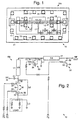
- Fig. 1 is a top view of a flip chip MMIC device 10 comprising an passive limiter 10a in accordance with the principles of the present invention.
- a gallium arsenide (GaAs) substrate 11 is provided on which the passive limiter 10a is formed.
- the passive limiter 10a comprises a plurality of limiter diodes 12 that are used as RF limiting devices.
- the passive limiter 10a also comprises a host substrate 21, which may be aluminum nitride, for example, disposed "above" the gallium arsenide substrate 11 in flip-chip fashion.
- a plurality of plated metallized hard, plated thermal bumps 14 are used to provide RF input/output connections between RF input/output pads 13 and bonding pads 15 (selected ones are shown using dashed lines) of the host substrate 21.
- a Plurality of thermal bumps 14 are also disposed between the limiter diodes 12 and other bonding pads 15 the host substrate 21.
- the thermal bumps 14 may have either a circular cross section or have a rectangular cross section.
- the thermal bumps 14 provide for improved heat dissipation and power protection.
- the passive limiter 10a also comprises a coplanar waveguide transmission line 17 coupled between input/output ports of the limiter 10a and the limiter diodes 12, thus eliminating the need for backside processing of the gallium arsenide substrate 11.
- the coplanar waveguide transmission line 17 is used in place of conventionally-used face-up microstrip transmission line.
- Gallium arsenide has many superior electrical properties compared to silicon. However, gallium arsenide is a poor thermal conductor. Because there is no backside processing of the gallium arsenide substrate 11, the flip chip gallium arsenide substrate 11 is 0,655 mm, 0.025" in thickness. Although mechanically robust in terms of physical handling issues, the 0.025" thick gallium arsenide substrate 11 falls short with regards to its thermal performance characteristics.
- 0.003" high plated silver thermal bumps 14 are used. By directly solder attaching the thermal bumps 14 to the host substrate 21 (aluminum nitride), an efficient thermal path is created, resulting in superior power handling performance of the limiter 10a.
- flip chip MMIC limiter devices 10a formed on gallium arsenide substrates 11 were fabricated with, and without, thermal bumps 14. Upon the completion of fabrication, various limiter devices 10a were measured using small signals to provide for insertion loss evaluation. These limiter devices 10a were subsequently mounted on aluminum nitride test substrates 21 to determine their power handling performance. It was found that the limiter devices 10a employing the thermal bumps 14 provided superior performance over those without the bumps 14.
- Fig. 2 is a schematic drawing illustrating a second flip chip MMIC device 10 comprising a transmit/receive absorptive switch 10b in accordance with the principles of the present invention.
- Fig. 2a is a layout of the transmit/receive absorptive switch 10b of Fig. 2.
- the transmit/receive switch 10b has an RF input (RF IN) that is coupled to an external antenna or radiator (not shown) by way of a circulator (not shown).
- the RF input (RF IN) is coupled to an input filter capacitor (C1).
- the input filter capacitor (C1) is coupled by way of first and second serially coupled ⁇ /8 coplanar waveguide transmission lines 17 to an RF output (RF OUT).
- the RF output (RF OUT) is coupled to a low noise amplifier (not shown).
- a first absorptive switch 30 comprising a field effect transistor 30 is coupled from a point between the two ⁇ /8 coplanar waveguide transmission lines 17 and ground and has an inductance (L1) coupled in parallel therewith.
- a second absorptive switch 30 comprising a field effect transistor 30 is coupled from a point between the second ⁇ /8 coplanar waveguide transmission line 17 and the RF output (RF OUT) and ground.
- First and second serially coupled absorptive switches 30 comprising field effect transistors (FET) 30 are coupled to a point between the input filter capacitor (C1) and the first ⁇ /8 coplanar waveguide transmission line 17 and a load (LOAD) having a parallel inductance (L3). Drain electrodes of the serially coupled absorptive switches 30 are coupled together.
- FET field effect transistors
- the first absorptive switch 30 has a source bridge 35 (or air bridge 35) disposed thereover that bridges between respective sources 32 and respective drains 34 of the field effect transistor 30.
- a thermal bump 14 (or shunt 14) is formed on top of the source bridge 35. The location of the source bridge 35 and thermal bump 14 are illustrated by the dashed box over the sources 32 and drains 34 of the first absorptive switch 30.
- a source bridge 35 (or air bridge 35) bridges between respective sources 32 of each of the serially coupled field effect transistors 30 forming the serially coupled absorptive switches 30. The location of the source bridge 35 and thermal bump 14 are illustrated by the dashed boxed over the sources of the two serially coupled switches 30.
- the physical structure relating to this aspect of the present invention is shown in and will be discussed in more detail below with regard to Fig. 3.
- the thermal bumps 14 of the respective field effect transistors 30 are coupled to bonding pads 15 on a host substrate 21.
- the transmit/receive absorptive switch 10b is coupled to the host substrate 21 in the manner of a flip-chip (i.e., upside down).
- the thermal bumps 14 are thus used to couple heat from the field effect transistors 30 to the host substrate 21.
- Control signals (TX) are coupled to respective gates 33 of each of the field effect transistors 30 by way of control circuitry including resistors whose values are selected to set the voltage levels at each of the gates 33 of the of the field effect transistors 30.
- the control signals switch the transmit/receive switch 10b from transmit mode to receive mode, and vice versa.
- Control signals (TX) are coupled to respective gates 33 of each of the field effect transistors 30 by way of control circuitry including resistors whose values are selected to set the voltage levels at each of the gates 33 of the of the field effect transistors 30.
- the control signals switch the transmit/receive switch 10b from transmit mode to receive mode; and vice versa.
- the switch 10b was designed to provide power protection in transmit mode. In the transmit mode, power received at the RF input (RF IN) is shunted through the serially coupled field effect transistors (FET) 30 into the load (LOAD). However, it has been determined during testing that the circuit topology of the transmit/receive absorptive switch 10b also provides a power protection in receive mode. In particular, in receive mode, which is the low insertion loss state of the switch 10b, the switch 10b acts as a limiter and provides a limited amount of power protection. This provides protection for the low noise amplifier in the event that unintended power is received
- Fig. 3 shows a perspective view of a portion of the thermal bumped field effect transistor 30 utilized in the transmit/receive absorptive switch 10b of Fig. 2 illustrating the primary inventive aspect of the present invention.
- the flip chip transmit/receive switch 10b uses thermal bumps 14 comprising plated metallized "hard" bumps 14 for I/O connections and thermal connections to the host substrate 21.
- the host substrate 17 may be aluminum nitride, for example.
- the embodiment of flip chip transmit/receive absorptive switch 10b is formed on a gallium arsenide substrate 11 and uses thermal bumps 14 to achieve improved heat dissipation and power protection.
- the flip chip transmit/receive switch 10b has a plurality of field effect transistors (FET) 30 that comprise the absorptive switches 30 that are formed on a surface of the gallium arsenide substrate 11.
- the field effect transistors 30 each comprise source, gate and drain electrodes 32, 33, 34, respectively, that are formed on the surface of the gallium arsenide substrate 11.
- a source bridge 35 (or air bridge 35) bridges between the respective sources 32 of each field effect transistor 30.
- the thermal bump 14 (comprising a shunt 14) is formed on top of the source bridge 35.
- the thermal bumps 14 of the respective field effect transistors 30 are coupled to bonding pads 15 on the host substrate 21.
- the flip chip MMIC transmit/receive absorptive switch 10b also uses coplanar waveguide transmission line 17 (in the manner shown in Fig. 1) coupled between RF input and output ports of the switch 10b and the field effect transistors 30, thus eliminating the need for processing the back side of the gallium arsenide substrate 11.
- the coplanar waveguide transmission line 17 is used in place of a conventionally-used face-up microstrip arrangement.
- gallium arsenide has many superior electrical properties with respect to silicon.
- gallium arsenide is a poor thermal conductor.
- the flip chip gallium arsenide substrate 11 may be fabricated to be 0.025" in thickness.
- mechanically robust in terms of handling issues 0.025" of gallium arsenide substrates falls short in regards to thermal performance characteristics.
- 0.003" high plated silver thermal bumps 14 are used.
- the key to the switch embodiment of the present invention is the placement of the thermal bumps 14 over the air bridge 35 which "stitches" the source pads 32 of each switch field effect transistor 30.
- the thermal bumps 14 By placing the thermal bumps 14 directly on the source bridge 35 of the field effect transistors 30, the RF performance characteristics of the field effect transistors 30 are not degraded by the presence of the bumps 14.
- accurate models of the field effect transistors 30 for design purposes can be obtained with, or without, the presence of the thermal bumps 14.
- an efficient thermal path is created, resulting in superior power handling performance of the transmit/receive switch 10b.
- flip chip transmit/receive MMIC switches 10b on gallium arsenide substrates 11 were fabricated with, and without, thermal bumps 14.
- both variants of the flip chip transmit/receive MMIC switches 10b were mounted on aluminum nitride test substrates 21 and rigorously tested.
- the test results of flip chip transmit/receive switches 10b with thermal bumps 14 is shown in Fig. 4.
- the flip chip transmit/receive switches 10b with thermal bumps 14 display at least twice the power handling performance compared to the variant without thermal bumps 14.
Landscapes
- Semiconductor Integrated Circuits (AREA)
Abstract
Description
- The present invention relates to a flip-chip gallium arsenide monolithic microwave integrated circuit device, comprising
a gallium arsenide substrate;
a plurality of RF devices disposed on the gallium arsenide substrate; and
a host substrate;
wherein a first plurality of thermal heat conducting bumps are disposed between said plurality of RF devices and bonding pads of the host substrate to couple the gallium arsenide substrate to the host substrate in flip-chip fashion. - Such a device is known, for instance, from US 5,708,283.
- Flip-chip technology involves methods used to interconnect semiconductor die to a host substrate. Generally, bumps (solder, or hard plated bumps) are used in place of wirebonds for I/O connections. Flip-chip bump interconnection technology is a concept that has been around for many years. Most of the past work in this technology area has concentrated on the use of solder bump technology in conjunction with silicon-based integrated circuits.
- A known prior art relating to the present flip-chip limiter is a conventional face-up limiter MMIC device. A known prior art relating to the present transmit/receive switch is a conventional face-up transmit/receive switch MMIC device. The limiter and face-up transmit/receive switch MMIC devices require full wafer processing, including costly backside processing such as wafer thinning, along with via and backside metallization. Because this design is based on conventional microstrip transmission line media, the performance of this circuit is very sensitive to backside processing, especially wafer thinning. Finally, and most importantly, gallium arsenide is not an excellent thermal conductor. Under high incident RF conditions, large amounts of heat will be seen at the locations of active device. This heat must then be dissipated through the gallium arsenide. It is this heat dissipation limitation which limits the power protection capability of the prior art.
- US 5,708,283, already mentioned at the outset, discloses a high power, flip-chip microwave monolithic integrated circuit assembly which employs thermally conductive bumps in order to improve heat dissipation from active areas. The thermal bumps are provided between RF devices like FETs, HEMTs, or HBTs, and
a host substrate. In one embodiment, an air bridge is shown which electrically interconnects source pads of field effect transistors. A bump is provided between the air bridge and the substrate. This document, however, does not disclose any details of the circuits employed in the assembly. - Another flip-chip integrated circuit is known from US 5,532,506. In one embodiment, this document discloses a flip-chip device employing coplanar waveguides. Additionally, use of air bridges is disclosed, wherein the air bridges are in thermal contact with a planar heat sink. This document, however, does not disclose use of thermal bumps in order to provide for heat dissipation.
- In view of this prior art, it is an objective of the present invention to provide for improved flip-chip MMIC devices formed on gallium arsenide that employ thermally bumped diode and field effect transistor devices. In particular, it is an objective of the present invention to improve heat dissipation for MMIC devices employing thermal bumps with minimum production effort and costs. Even more particularly, it is an objective of the present invention to provide for improved flip-chip limiter monolithic microwave integrated circuits formed on gallium arsenide employing thermal bumped diode devices. Yet another particular objective of the present invention is to provide for improved transmit/receive switch monolithic microwave integrated circuit formed on gallium arsenide employing thermal bumped FET devices.
- The objective is achieved by a flip-chip device as mentioned at the outset, characterized in that a second plurality of heat conducting thermal bumps are disposed between RF input/output pads of said device and bonding pads of the host substrate, and a coplanar waveguide transmission line is coupled between said RF input/output pads of the device and the RF devices.
- The present inventions provides for flip-chip monolithic microwave integrated circuit (MMIC) devices formed on gallium arsenide (GaAs) and use thermally bumped diode and FET devices to achieve improved heat dissipation and power protection. Flip-chip limiter MMIC devices and transmit/receive switch MMIC devices are specifically provided by the present invention. The flip-chip gallium arsenide limiter and transmit/receive switch MMIC devices use plated metallized bumps for both I/O connections and for thermal connections to a host substrate (aluminum nitride). The present invention also incorporates coplanar waveguide transmission line eliminating the need for backside processing of the gallium arsenide substrates.
- More specifically, one embodiment of the present invention comprises a flip-chip passive limiter monolithic microwave integrated circuit device formed on gallium arsenide employing thermal bumped diode devices. The flip-chip gallium arsenide limiter MMIC device uses plated metallized "hard" bumps for RF input/output connections to a host substrate (aluminum nitride). The passive limiter also incorporates coplanar waveguide transmission media, thus eliminating the need for backside processing.
- The passive limiter is utilized as built-in full-time protection for transmit/receive modules, which protect sensitive devices in the receive path from high RF environments. The reflective limiter MMIC device is "flip" mounted on the host substrate (aluminum nitride) using plated bumps for RF in/out connections to the host substrate. A further improvement of this embodiment involves the structure and method of landing plated metallized bumps over a bridge of diodes (peak hot zones), allowing a direct thermal path away from active regions. By utilizing thermal bumps directly over the hot zones, the limiter can withstand much greater amounts of incident RF power in comparison to face-up MMIC devices without thermal bumps. In addition, the coplanar waveguide transmission line media eliminates the need for a ground plane on the backside of the MMIC device. Therefore, no backside processing steps (i.e., wafer thinning, via and backside metallization) are required. In doing so, wafer line yields are improved, and the performance sensitivity to gallium arsenide substrate thickness is eliminated.
- The passive limiter is a reflective limiter, and the circuit must handle large amounts of RF energy. Large amounts of incident power are absorbed by the diode because of its series resistance. Hence, the diode junction temperature is a key factor in terms of performance of the limiter. An advantage of the present invention stems from the application of thermal bumps over the hot zones (diodes) of the limiter. The use of thermal bumps over the diodes provides for a direct thermal path away from the device. In doing so, the power handling of the limiter is dramatically improved. This technique can be applied to any diode based limiter, including those using MIN and PIN diodes. Since a uniplanar design approach (using coplanar waveguide transmission line media) is employed, no backside processing is required. Therefore, the performance of the flip chip limiter is not susceptible to variations in wafer thinning, and the negative impact of via inductance. The use of flip chips also produce assembly and cost benefits.
- A second embodiment of the present invention provides for a transmit/receive switch monolithic microwave integrated circuit device formed on Gallium Arsenide employing thermal bumped FET devices. The transmit/receive switch device is utilized to provide built-in protection for transmit/receive modules, protecting sensitive devices in the receive path from high RF environments. This absorptive transmit/receive switch MMIC is "flip" mounted on the host substrate (aluminum nitride) using plated bumps for I/O connections to the host substrate. Again, a further improvement of this embodiment involves the structure and method of landing plated metallized bumps over the source bridge of FET devices (peak hot zones), allowing a direct thermal path away from the active FET regions. By utilizing thermal bumps directly over the hot zones of this absorptive switch, the device can withstand much greater amounts of incident RF power in comparison to face-up MMIC devices without thermal bumps. In addition, the coplanar waveguide transmission line media eliminates the need for a ground plane on the backside of the MMIC device. Therefore, no backside processing steps (i.e., wafer thinning, via and backside metallization) are required. Thus, wafer line yields are improved, and the sensitivity of the performance of the switches to gallium arsenide substrate thickness is eliminated.
- The transmit/receive switch device is an absorptive switch with on-chip loads, and the circuit must handle large amounts of RF energy. An advantage of the present invention stems from the use of thermal bumps over the hot zones of the switch. The use of thermal bumps over the source bridge of the FET devices allows a direct thermal path away from the device. Thus, the power handling of the switch is improved dramatically. This improvement comes without the need for costly changes to established FET technology processes for power handling performance. Since a uniplanar design approach (by use of coplanar waveguide transmission line media) is employed, no backside processing is required. Therefore, the performance of the flip chip switch is not susceptible to variations in wafer thinning, and the negative impact of via inductance. This susceptibility to backside processing is evident in conventional face-up MMIC variants. The use of flip chips also result in assembly and cost benefits.
- The present flip chip limiter MMIC and transmit/receive switch MMIC devices may be preferably used in transmit/receive modules. The transmit/receive modules are basic building blocks of airborne and ground based electronically-steered antenna arrays.
- The various features and advantages of the present invention may be more readily understood with reference to the following detailed description taken in conjunction with the accompanying drawings, wherein like reference numerals designate like structural elements, and in which:
- Fig. 1 is a top view of a flip chip MMIC device comprising a passive limiter in accordance with the principles of the present invention;
- Fig. 2 is a schematic drawing of a flip chip MMIC device illustrating a transmit/receive absorptive switch in accordance with the principles of the present invention;
- Fig. 2a is a layout of the transmit/receive absorptive switch of Fig. 2;
- Fig. 3 shows a perspective view of a portion of the thermal bumped field effect transistor utilized in the transmit/receive absorptive switch of Fig. 2; and
- Fig. 4 is a graph showing the improved performance of the transmit/receive absorptive switch of Figs. 2 and 3.
-
- Referring to the drawing figures, Fig. 1 is a top view of a flip
chip MMIC device 10 comprising anpassive limiter 10a in accordance with the principles of the present invention. A gallium arsenide (GaAs)substrate 11 is provided on which thepassive limiter 10a is formed. Thepassive limiter 10a comprises a plurality oflimiter diodes 12 that are used as RF limiting devices. Thepassive limiter 10a also comprises ahost substrate 21, which may be aluminum nitride, for example, disposed "above" thegallium arsenide substrate 11 in flip-chip fashion. - A plurality of plated metallized hard, plated
thermal bumps 14 are used to provide RF input/output connections between RF input/output pads 13 and bonding pads 15 (selected ones are shown using dashed lines) of thehost substrate 21. A Plurality ofthermal bumps 14 are also disposed between thelimiter diodes 12 andother bonding pads 15 thehost substrate 21. The thermal bumps 14 may have either a circular cross section or have a rectangular cross section. The thermal bumps 14 provide for improved heat dissipation and power protection. Thepassive limiter 10a also comprises a coplanarwaveguide transmission line 17 coupled between input/output ports of thelimiter 10a and thelimiter diodes 12, thus eliminating the need for backside processing of thegallium arsenide substrate 11. The coplanarwaveguide transmission line 17 is used in place of conventionally-used face-up microstrip transmission line. - One of the primary limiting factors in the power handling capability of conventional limiters is due to failures in active diode regions. Device performance degradation is accelerated due to thermal-related failure mechanisms. During use, high incident RF levels cause large levels of current to be drawn by the
limiter diodes 12. A substantial part of the incident RF power is absorbed by thelimiter diodes 12 because of their series resistance. The key to good power handling is the ability to efficiently dissipate this heat away from the locations of thelimiter diodes 12. This is achieved using the thermal bumps 14. - Gallium arsenide has many superior electrical properties compared to silicon. However, gallium arsenide is a poor thermal conductor. Because there is no backside processing of the
gallium arsenide substrate 11, the flip chipgallium arsenide substrate 11 is 0,655 mm, 0.025" in thickness. Although mechanically robust in terms of physical handling issues, the 0.025" thickgallium arsenide substrate 11 falls short with regards to its thermal performance characteristics. To efficiently conduct heat away from thelimiter diodes 12 76,2 µm, 0.003" high plated silverthermal bumps 14 are used. By directly solder attaching thethermal bumps 14 to the host substrate 21 (aluminum nitride), an efficient thermal path is created, resulting in superior power handling performance of thelimiter 10a. - As proof of this design concept, flip chip
MMIC limiter devices 10a formed ongallium arsenide substrates 11 were fabricated with, and without, thermal bumps 14. Upon the completion of fabrication,various limiter devices 10a were measured using small signals to provide for insertion loss evaluation. Theselimiter devices 10a were subsequently mounted on aluminumnitride test substrates 21 to determine their power handling performance. It was found that thelimiter devices 10a employing thethermal bumps 14 provided superior performance over those without thebumps 14. - Fig. 2 is a schematic drawing illustrating a second flip
chip MMIC device 10 comprising a transmit/receiveabsorptive switch 10b in accordance with the principles of the present invention. Fig. 2a is a layout of the transmit/receiveabsorptive switch 10b of Fig. 2. The transmit/receiveswitch 10b has an RF input (RF IN) that is coupled to an external antenna or radiator (not shown) by way of a circulator (not shown). The RF input (RF IN) is coupled to an input filter capacitor (C1). The input filter capacitor (C1) is coupled by way of first and second serially coupled λ/8 coplanarwaveguide transmission lines 17 to an RF output (RF OUT). The RF output (RF OUT) is coupled to a low noise amplifier (not shown). A firstabsorptive switch 30 comprising afield effect transistor 30 is coupled from a point between the two λ/8 coplanarwaveguide transmission lines 17 and ground and has an inductance (L1) coupled in parallel therewith. A secondabsorptive switch 30 comprising afield effect transistor 30 is coupled from a point between the second λ/8 coplanarwaveguide transmission line 17 and the RF output (RF OUT) and ground. First and second serially coupledabsorptive switches 30 comprising field effect transistors (FET) 30 are coupled to a point between the input filter capacitor (C1) and the first λ/8 coplanarwaveguide transmission line 17 and a load (LOAD) having a parallel inductance (L3). Drain electrodes of the serially coupledabsorptive switches 30 are coupled together. - In accordance with a preferred embodiment the first
absorptive switch 30 has a source bridge 35 (or air bridge 35) disposed thereover that bridges betweenrespective sources 32 andrespective drains 34 of thefield effect transistor 30. A thermal bump 14 (or shunt 14) is formed on top of thesource bridge 35. The location of thesource bridge 35 andthermal bump 14 are illustrated by the dashed box over thesources 32 and drains 34 of the firstabsorptive switch 30. Furthermore, a source bridge 35 (or air bridge 35) bridges betweenrespective sources 32 of each of the serially coupledfield effect transistors 30 forming the serially coupled absorptive switches 30. The location of thesource bridge 35 andthermal bump 14 are illustrated by the dashed boxed over the sources of the two serially coupled switches 30. The physical structure relating to this aspect of the present invention is shown in and will be discussed in more detail below with regard to Fig. 3. - However, as is illustrated in Fig. 3, the
thermal bumps 14 of the respectivefield effect transistors 30 are coupled tobonding pads 15 on ahost substrate 21. Thus, the transmit/receiveabsorptive switch 10b is coupled to thehost substrate 21 in the manner of a flip-chip (i.e., upside down). The thermal bumps 14 are thus used to couple heat from thefield effect transistors 30 to thehost substrate 21. - Control signals (TX) are coupled to
respective gates 33 of each of thefield effect transistors 30 by way of control circuitry including resistors whose values are selected to set the voltage levels at each of thegates 33 of the of thefield effect transistors 30. The control signals switch the transmit/receiveswitch 10b from transmit mode to receive mode, and vice versa. - Control signals (TX) are coupled to
respective gates 33 of each of thefield effect transistors 30 by way of control circuitry including resistors whose values are selected to set the voltage levels at each of thegates 33 of the of thefield effect transistors 30. The control signals switch the transmit/receiveswitch 10b from transmit mode to receive mode; and vice versa. - In testing the transmit/receive
absorptive switch 10b shown in Fig. 2, it has been found that this topology produces unexpected beneficial results. Theswitch 10b was designed to provide power protection in transmit mode. In the transmit mode, power received at the RF input (RF IN) is shunted through the serially coupled field effect transistors (FET) 30 into the load (LOAD). However, it has been determined during testing that the circuit topology of the transmit/receiveabsorptive switch 10b also provides a power protection in receive mode. In particular, in receive mode, which is the low insertion loss state of theswitch 10b, theswitch 10b acts as a limiter and provides a limited amount of power protection. This provides protection for the low noise amplifier in the event that unintended power is received - Fig. 3 shows a perspective view of a portion of the thermal bumped
field effect transistor 30 utilized in the transmit/receiveabsorptive switch 10b of Fig. 2 illustrating the primary inventive aspect of the present invention. The flip chip transmit/receiveswitch 10b usesthermal bumps 14 comprising plated metallized "hard" bumps 14 for I/O connections and thermal connections to thehost substrate 21. Thehost substrate 17 may be aluminum nitride, for example. - The embodiment of flip chip transmit/receive
absorptive switch 10b is formed on agallium arsenide substrate 11 and usesthermal bumps 14 to achieve improved heat dissipation and power protection. The flip chip transmit/receiveswitch 10b has a plurality of field effect transistors (FET) 30 that comprise theabsorptive switches 30 that are formed on a surface of thegallium arsenide substrate 11. Thefield effect transistors 30 each comprise source, gate and drainelectrodes gallium arsenide substrate 11. A source bridge 35 (or air bridge 35) bridges between therespective sources 32 of eachfield effect transistor 30. The thermal bump 14 (comprising a shunt 14) is formed on top of thesource bridge 35. - The thermal bumps 14 of the respective
field effect transistors 30 are coupled tobonding pads 15 on thehost substrate 21. The flip chip MMIC transmit/receiveabsorptive switch 10b also uses coplanar waveguide transmission line 17 (in the manner shown in Fig. 1) coupled between RF input and output ports of theswitch 10b and thefield effect transistors 30, thus eliminating the need for processing the back side of thegallium arsenide substrate 11. The coplanarwaveguide transmission line 17 is used in place of a conventionally-used face-up microstrip arrangement. - One of the primary limiting factors in the power handling capability of conventional FET-based switches is due failure in the active switch FET regions. Device performance degradation is accelerated due to thermal-related failure mechanisms. In use, high incident RF levels cause large levels of heat to localize in the active switch FET regions. The key to good power handling is the ability to efficiently dissipate this heat away from the active switch FET locations. This is achieved using the present invention.
- As was stated above, gallium arsenide has many superior electrical properties with respect to silicon. However, gallium arsenide is a poor thermal conductor. Because there is no backside processing of the
gallium arsenide substrate 11 in the present invention, the flip chipgallium arsenide substrate 11 may be fabricated to be 0.025" in thickness. Although mechanically robust in terms of handling issues, 0.025" of gallium arsenide substrates falls short in regards to thermal performance characteristics. To efficiently conduct heat away from thefield effect transistors 30, 0.003" high plated silverthermal bumps 14 are used. - The key to the switch embodiment of the present invention is the placement of the
thermal bumps 14 over theair bridge 35 which "stitches" thesource pads 32 of each switchfield effect transistor 30. By placing thethermal bumps 14 directly on thesource bridge 35 of thefield effect transistors 30, the RF performance characteristics of thefield effect transistors 30 are not degraded by the presence of thebumps 14. Thus, accurate models of thefield effect transistors 30 for design purposes can be obtained with, or without, the presence of the thermal bumps 14. By directly solder attaching of thethermal bumps 14 to thehost substrate 21, an efficient thermal path is created, resulting in superior power handling performance of the transmit/receiveswitch 10b. - To prove out this design concept, various flip chip transmit/receive
MMIC switches 10b ongallium arsenide substrates 11 were fabricated with, and without, thermal bumps 14. Upon completion of fabrication, both variants of the flip chip transmit/receiveMMIC switches 10b were mounted on aluminumnitride test substrates 21 and rigorously tested. The test results of flip chip transmit/receiveswitches 10b withthermal bumps 14 is shown in Fig. 4. In addition to having low insertion loss characteristics, the flip chip transmit/receiveswitches 10b withthermal bumps 14 display at least twice the power handling performance compared to the variant without thermal bumps 14. - Thus, improved flip chip gallium arsenide MMIC devices that employ thermally bumped diode and field effect transistor (FET) devices have been disclosed. It is to be understood that the described embodiments are merely illustrative of some of the many specific embodiments that represent applications of the principles of the present invention. Clearly, numerous and other arrangements can be readily devised by those skilled in the art without departing from the scope of the invention.
Claims (9)
- A flip-chip gallium arsenide monolithic microwave integrated circuit device (10), comprising:wherein a first plurality of thermal heat conducting bumps (14) are disposed between said plurality of RF devices (12) and bonding pads (15) of the host substrate (21) to couple the gallium arsenide substrate (11) to the host substrate (21) in flip-chip fashion;a gallium arsenide substrate (11);a plurality of RF devices (12, 30) disposed on the gallium arsenide substrate (11); anda host substrate (21);
characterized by a second plurality of heat conducting thermal bumps (14) being disposed between RF input/output pads (13) of said device (10; 10a, 10b) and bonding pads (15) of the host substrate (21), and
a coplanar waveguide transmission line (17) being coupled between said RF input/output pads (13) of the device (10) and the RF devices (12). - The device (10) of claim 1, characterized in that the host substrate (21) comprises an aluminum nitride substrate (21).
- The device (10) of claim 1, characterized in that the thermal bumps (14) have a circular cross section.
- The device (10) of claim 1, characterized in that the thermal bumps (14) have a rectangular cross section.
- The device (10) of claim 1, characterized in that the plurality of RF devices (12) comprise passive diodes (12).
- The device (10) of claim 1, characterized in that the plurality of RF devices (12) comprise field effect transistors (30).
- The device (10) of claim 1, characterized by an air bridge (35) coupled between sources (32) of selected field effect transistors (30) and the thermal bumps (14) disposed over the selected field effect transistors (30).
- The device (10) of claim 1, characterized by:an RF input (RF IN) and an RF output (RF OUT);and wherein the coplanar waveguide transmission line (17) comprises first and second serially coupled coplanar waveguide transmission lines (17, 17), wherein one end of the first coplanar waveguide transmission line (17) is coupled to the RF input (RF IN) and wherein one end of the second λ/8 coplanar waveguide transmission line (17) is coupled to the RF output (RF OUT);and wherein the plurality of RF devices (12) comprise:a first absorptive switch (30) coupled from a point between the first and second λ/8 coplanar waveguide transmission lines (17, 17) and ground;a second absorptive switch (30) coupled from a point between said end of the second λ/8 coplanar waveguide transmission line (17) and the RF output (RF OUT) and ground;first and second serially coupled absorptive switches (30, 30) coupled between the RF input (RF IN) and a load; andcontrol circuitry (TX) coupled to the switches (30) for coupling control signals thereto that switch the device (10) between transmit and receive modes.
- The device (10) of claim 8, characterized in that each of the absorptive switches (30) comprises a field effect transistor (30).
Applications Claiming Priority (3)
| Application Number | Priority Date | Filing Date | Title |
|---|---|---|---|
| US09/090,700 US5990757A (en) | 1998-06-05 | 1998-06-05 | Gallium arsenide monolithic microwave integrated circuits employing thermally bumped devices |
| US90700 | 1998-06-05 | ||
| PCT/US1999/012435 WO1999063595A1 (en) | 1998-06-05 | 1999-06-03 | Gallium arsenide monolithic microwave integrated circuits employing thermally bumped devices |
Publications (2)
| Publication Number | Publication Date |
|---|---|
| EP1008180A1 EP1008180A1 (en) | 2000-06-14 |
| EP1008180B1 true EP1008180B1 (en) | 2002-09-11 |
Family
ID=22223897
Family Applications (1)
| Application Number | Title | Priority Date | Filing Date |
|---|---|---|---|
| EP99927203A Expired - Lifetime EP1008180B1 (en) | 1998-06-05 | 1999-06-03 | Gallium arsenide monolithic microwave integrated circuits employing thermally bumped devices |
Country Status (4)
| Country | Link |
|---|---|
| US (1) | US5990757A (en) |
| EP (1) | EP1008180B1 (en) |
| DE (1) | DE69902862T2 (en) |
| WO (1) | WO1999063595A1 (en) |
Families Citing this family (16)
| Publication number | Priority date | Publication date | Assignee | Title |
|---|---|---|---|---|
| US6507110B1 (en) | 2000-03-08 | 2003-01-14 | Teledyne Technologies Incorporated | Microwave device and method for making same |
| US6518589B2 (en) | 2000-06-22 | 2003-02-11 | Progressant Technologies, Inc. | Dual mode FET & logic circuit having negative differential resistance mode |
| US6968157B2 (en) * | 2001-08-22 | 2005-11-22 | University Of Maryland | System and method for protecting devices from interference signals |
| US6933603B2 (en) * | 2002-07-11 | 2005-08-23 | Teledyne Technologies Incorporated | Multi-substrate layer semiconductor packages and method for making same |
| US6747484B1 (en) * | 2003-04-22 | 2004-06-08 | Raytheon Company | Radio frequency limiter circuit |
| US7656236B2 (en) | 2007-05-15 | 2010-02-02 | Teledyne Wireless, Llc | Noise canceling technique for frequency synthesizer |
| US8269344B2 (en) * | 2008-03-28 | 2012-09-18 | Broadcom Corporation | Method and system for inter-chip communication via integrated circuit package waveguides |
| US8179045B2 (en) | 2008-04-22 | 2012-05-15 | Teledyne Wireless, Llc | Slow wave structure having offset projections comprised of a metal-dielectric composite stack |
| US8274147B2 (en) * | 2008-06-19 | 2012-09-25 | Broadcom Corporation | Method and system for intra-printed circuit board communication via waveguides |
| US8450846B2 (en) * | 2008-06-19 | 2013-05-28 | Broadcom Corporation | Method and system for communicating via flip-chip die and package waveguides |
| US7969001B2 (en) | 2008-06-19 | 2011-06-28 | Broadcom Corporation | Method and system for intra-chip waveguide communication |
| WO2012070987A1 (en) | 2010-11-22 | 2012-05-31 | Saab Ab | Power supply arrangement for distribution of power |
| US9202660B2 (en) | 2013-03-13 | 2015-12-01 | Teledyne Wireless, Llc | Asymmetrical slow wave structures to eliminate backward wave oscillations in wideband traveling wave tubes |
| US12531524B2 (en) | 2020-06-25 | 2026-01-20 | Macom Technology Solutions Holdings, Inc. | Multi-zone radio frequency transistor amplifiers |
| US11533024B2 (en) * | 2020-06-25 | 2022-12-20 | Wolfspeed, Inc. | Multi-zone radio frequency transistor amplifiers |
| CN113659944A (en) * | 2021-07-13 | 2021-11-16 | 中国电子科技集团公司第二十九研究所 | Carrier plate type microwave power amplifier capable of being tested on chip |
Family Cites Families (7)
| Publication number | Priority date | Publication date | Assignee | Title |
|---|---|---|---|---|
| US5047829A (en) * | 1986-10-30 | 1991-09-10 | Texas Instruments Incorporated | Monolithic p-i-n diode limiter |
| US4951014A (en) * | 1989-05-26 | 1990-08-21 | Raytheon Company | High power microwave circuit packages |
| US5510758A (en) * | 1993-04-07 | 1996-04-23 | Matsushita Electric Industrial Co., Ltd. | Multilayer microstrip wiring board with a semiconductor device mounted thereon via bumps |
| US5521406A (en) * | 1994-08-31 | 1996-05-28 | Texas Instruments Incorporated | Integrated circuit with improved thermal impedance |
| US5610563A (en) * | 1994-09-26 | 1997-03-11 | Endgate Corporation | Slot line to CPW circuit structure |
| US5528203A (en) * | 1994-09-26 | 1996-06-18 | Endgate Corporation | Coplanar waveguide-mounted flip chip |
| EP0708481A3 (en) * | 1994-10-20 | 1997-04-02 | Hughes Aircraft Co | Improved thermal bumps for high power monolithic integrated circuits of the flip chip type and manufacturing process |
-
1998
- 1998-06-05 US US09/090,700 patent/US5990757A/en not_active Expired - Lifetime
-
1999
- 1999-06-03 WO PCT/US1999/012435 patent/WO1999063595A1/en not_active Ceased
- 1999-06-03 EP EP99927203A patent/EP1008180B1/en not_active Expired - Lifetime
- 1999-06-03 DE DE69902862T patent/DE69902862T2/en not_active Expired - Lifetime
Also Published As
| Publication number | Publication date |
|---|---|
| US5990757A (en) | 1999-11-23 |
| DE69902862D1 (en) | 2002-10-17 |
| WO1999063595A1 (en) | 1999-12-09 |
| DE69902862T2 (en) | 2003-05-08 |
| EP1008180A1 (en) | 2000-06-14 |
Similar Documents
| Publication | Publication Date | Title |
|---|---|---|
| US5990757A (en) | Gallium arsenide monolithic microwave integrated circuits employing thermally bumped devices | |
| US5614442A (en) | Method of making flip-chip microwave integrated circuit | |
| JP3487639B2 (en) | Semiconductor device | |
| US6424006B1 (en) | Semiconductor component | |
| US7005734B2 (en) | Double-sided cooling isolated packaged power semiconductor device | |
| US6809416B1 (en) | Package for integrated circuit with thermal vias and method thereof | |
| JPH0856113A (en) | Millimeter wave detector | |
| WO2002086971A3 (en) | Multichip module fabricated on a semiconductor or dielectric wafer and method for manufacturing same | |
| US5708283A (en) | Flip chip high power monolithic integrated circuit thermal bumps | |
| US5990499A (en) | Integrated semiconductor circuit | |
| KR100292904B1 (en) | Semiconductor device | |
| US9000496B1 (en) | Source bridge for cooling and/or external connection | |
| Böck et al. | Low-cost eWLB packaging for automotive radar MMICs in the 76–81 GHz range | |
| US6933603B2 (en) | Multi-substrate layer semiconductor packages and method for making same | |
| CN218827128U (en) | Power module and packaging structure thereof | |
| JP3920629B2 (en) | Semiconductor device | |
| US12424594B2 (en) | Integrated diamond substrate for thermal management | |
| US6094114A (en) | Slotline-to-slotline mounted flip chip | |
| KR101148888B1 (en) | Mmic having back-side multi-layer signal routing | |
| US6545350B2 (en) | Integrated circuit packages and the method for the same | |
| Bahl et al. | C-band 10 W MMIC class-A amplifier manufactured using the refractory SAG process | |
| JP3196752B2 (en) | Semiconductor integrated circuit device and manufacturing method thereof | |
| Cisco | Flip Chip Power MMICS Packaging Technology | |
| Bump | interconnection suitable for millimeter wave use and for microwave power devices. A properly designed custom bump can reduce thermal resistance to half that of face-up mounting. Examples of solid metal and thermal bumps are shown in Figure 2, together with a mounted flip chip assembly. | |
| US6670674B2 (en) | Transistor and power amplifier with improved bandwidth |
Legal Events
| Date | Code | Title | Description |
|---|---|---|---|
| PUAI | Public reference made under article 153(3) epc to a published international application that has entered the european phase |
Free format text: ORIGINAL CODE: 0009012 |
|
| AK | Designated contracting states |
Kind code of ref document: A1 Designated state(s): DE FR GB |
|
| 17P | Request for examination filed |
Effective date: 20000519 |
|
| 17Q | First examination report despatched |
Effective date: 20010330 |
|
| GRAG | Despatch of communication of intention to grant |
Free format text: ORIGINAL CODE: EPIDOS AGRA |
|
| GRAG | Despatch of communication of intention to grant |
Free format text: ORIGINAL CODE: EPIDOS AGRA |
|
| GRAH | Despatch of communication of intention to grant a patent |
Free format text: ORIGINAL CODE: EPIDOS IGRA |
|
| GRAH | Despatch of communication of intention to grant a patent |
Free format text: ORIGINAL CODE: EPIDOS IGRA |
|
| GRAA | (expected) grant |
Free format text: ORIGINAL CODE: 0009210 |
|
| AK | Designated contracting states |
Kind code of ref document: B1 Designated state(s): DE FR GB |
|
| REG | Reference to a national code |
Ref country code: GB Ref legal event code: FG4D |
|
| REF | Corresponds to: |
Ref document number: 69902862 Country of ref document: DE Date of ref document: 20021017 |
|
| ET | Fr: translation filed | ||
| PLBE | No opposition filed within time limit |
Free format text: ORIGINAL CODE: 0009261 |
|
| STAA | Information on the status of an ep patent application or granted ep patent |
Free format text: STATUS: NO OPPOSITION FILED WITHIN TIME LIMIT |
|
| 26N | No opposition filed |
Effective date: 20030612 |
|
| REG | Reference to a national code |
Ref country code: FR Ref legal event code: PLFP Year of fee payment: 18 |
|
| REG | Reference to a national code |
Ref country code: FR Ref legal event code: PLFP Year of fee payment: 19 |
|
| PGFP | Annual fee paid to national office [announced via postgrant information from national office to epo] |
Ref country code: GB Payment date: 20170531 Year of fee payment: 19 Ref country code: FR Payment date: 20170511 Year of fee payment: 19 Ref country code: DE Payment date: 20170530 Year of fee payment: 19 |
|
| REG | Reference to a national code |
Ref country code: DE Ref legal event code: R119 Ref document number: 69902862 Country of ref document: DE |
|
| GBPC | Gb: european patent ceased through non-payment of renewal fee |
Effective date: 20180603 |
|
| PG25 | Lapsed in a contracting state [announced via postgrant information from national office to epo] |
Ref country code: GB Free format text: LAPSE BECAUSE OF NON-PAYMENT OF DUE FEES Effective date: 20180603 Ref country code: DE Free format text: LAPSE BECAUSE OF NON-PAYMENT OF DUE FEES Effective date: 20190101 Ref country code: FR Free format text: LAPSE BECAUSE OF NON-PAYMENT OF DUE FEES Effective date: 20180630 |