EP1004883A1 - Breitbandiges hochfrequenz-leistungsdetektionselement und leistungsdetektor unter vewendung eines solchen elements - Google Patents
Breitbandiges hochfrequenz-leistungsdetektionselement und leistungsdetektor unter vewendung eines solchen elements Download PDFInfo
- Publication number
- EP1004883A1 EP1004883A1 EP98921866A EP98921866A EP1004883A1 EP 1004883 A1 EP1004883 A1 EP 1004883A1 EP 98921866 A EP98921866 A EP 98921866A EP 98921866 A EP98921866 A EP 98921866A EP 1004883 A1 EP1004883 A1 EP 1004883A1
- Authority
- EP
- European Patent Office
- Prior art keywords
- thin
- film
- substrate
- film resistor
- signal
- Prior art date
- Legal status (The legal status is an assumption and is not a legal conclusion. Google has not performed a legal analysis and makes no representation as to the accuracy of the status listed.)
- Withdrawn
Links
Images


Classifications
-
- G—PHYSICS
- G01—MEASURING; TESTING
- G01R—MEASURING ELECTRIC VARIABLES; MEASURING MAGNETIC VARIABLES
- G01R21/00—Arrangements for measuring electric power or power factor
- G01R21/06—Arrangements for measuring electric power or power factor by measuring current and voltage
- G01R21/07—Arrangements for measuring electric power or power factor by measuring current and voltage in circuits having distributed constants
-
- G—PHYSICS
- G01—MEASURING; TESTING
- G01R—MEASURING ELECTRIC VARIABLES; MEASURING MAGNETIC VARIABLES
- G01R21/00—Arrangements for measuring electric power or power factor
- G01R21/02—Arrangements for measuring electric power or power factor by thermal methods, e.g. calorimetric
- G01R21/04—Arrangements for measuring electric power or power factor by thermal methods, e.g. calorimetric in circuits having distributed constants
-
- G—PHYSICS
- G01—MEASURING; TESTING
- G01R—MEASURING ELECTRIC VARIABLES; MEASURING MAGNETIC VARIABLES
- G01R22/00—Arrangements for measuring time integral of electric power or current, e.g. electricity meters
-
- H—ELECTRICITY
- H03—ELECTRONIC CIRCUITRY
- H03F—AMPLIFIERS
- H03F2200/00—Indexing scheme relating to amplifiers
- H03F2200/261—Amplifier which being suitable for instrumentation applications
Definitions
- the present invention relates to a power detecting element for detecting the power of a wide-band RF signal and a power detecting device using the same and, more particularly, to a wide-band RF signal power detecting element which has an improved frequency characteristic and can be easily manufactured, and a power detecting device using the same.
- thermocouple system which allows a resistor to absorb a signal and detects heat generated by the resistor by using a thermocouple.
- the diode detecting system has the advantage that a response is obtained with almost no delay when an input signal is supplied to the diode.
- This diode detecting system has the problem that the detection accuracy is low because the system is readily influenced by the signal waveform and the signal level.
- junction capacitance of the diode makes it difficult for the diode detecting system to detect the power of a RF signal of millimeter waves or more.
- thermocouple system cannot achieve such high-speed responses as in the diode detecting system, because heat is generated by supplying a signal to the resistor.
- thermocouple system however, has the advantage that the system can accurately detect the power of a signal without being influenced by the signal waveform.
- the present applicant has disclosed a power detector (element) and a power detecting device using this thermocouple system in International Publication No. WO88/03319 (Japanese Patent Application No. 62-506672).
- this power detector includes a first thermocouple 4A and a second thermocouple 4B formed on an insulating substrate 1.
- the first thermocouple 4A is formed by connecting a metal thin-film conductor 3A to a silicon germanium mixed-crystal thin film 2A.
- the second thermocouple 4B is formed by connecting a metal thin-film conductor 3B to a silicon germanium mixed-crystal thin film 2B.
- the silicon germanium mixed-crystal thin film of the first thermocouple 4A and the metal thin-film conductor 3B of the second thermocouple 4B are formed parallel to oppose each other.
- End portions of the silicon germanium mixed-crystal thin film 2A of the first thermocouple 4A and the metal thin-film conductor 3B of the second thermocouple 4B are connected by a first electrode 5.
- a second electrode 6 is connected to the metal thin-film conductor 3A of the first thermocouple 4A.
- a third electrode 7 is connected to the silicon germanium mixed-crystal thin film 2B of the second thermocouple 4B.
- thermocouples 4A and 4B are added and output to between the second and third electrodes 6 and 7.
- Beam lead electrodes 8, 9, and 10 for decreasing the thermal resistance in a cold junction between the first and second thermocouples 4A and 4B are connected to the first, second, and third electrodes 5, 6, and 7, respectively.
- This power detector is mounted on a dielectric substrate 11 of a power detecting device shown in FIG. 21.
- This dielectric substrate 11 has a transmission line composed of a central conductor 12 having a predetermined width and external conductors 13A and 13B formed parallel with a predetermined spacing between them on the two sides of the central conductor 12.
- the beam lead electrode 8 of this power detector 14 constructed as shown in FIG. 20 is connected to the central conductor 12 on the dielectric substrate 11.
- the beam lead electrode 9 of the power detector 14 is connected to ground (GND) which communicates with the external conductor 13B on the dielectric substrate 11.
- the beam lead electrode 10 of the power detector 14 is connected to an output conductor 15 on the dielectric substrate 11.
- the central conductor 12 on the dielectric substrate 11 is connected to a connecting portion 17 via a coupling capacitor 16.
- the output conductor 15 on the dielectric substrate 11 is connected to ground (GND) which communicates with the external conductor 13A via a bypass capacitor 18.
- a lead line 19A for central conductor output is connected to the output conductor 15.
- a lead line 19B for GND output is connected to the ground (GND) which communicates with the external conductor 13B.
- FIG. 22 shows an equivalent circuit of this power detecting device.
- thermocouples 4A and 4B a signal S to be measured input from the connecting portion 17 is supplied to the two thermocouples 4A and 4B via the coupling capacitor 16, and these two thermocouples 4A and 4B generate heat.
- thermocouple system In addition to the above system (so-called direct heating type), a so-called indirect heating system is also proposed as the thermocouple system.
- a resistor for converting a power signal to be measured into heat i.e., an input resistor
- a thermocouple for detecting a temperature rise resulting from the heat generated by this resistor
- thermocouple has a longer response time than that of the direct heating type thermocouple.
- the number of thermocouples can be arbitrarily increased independently of the resistor, and a signal having magnitude directly proportional to the number of these thermocouples can be output.
- thermocouple has the advantage that high detectivity is obtained.
- Thermocouples having frequency characteristics of about 20-odd GHz have been realized.
- thermocouples themselves to cause these thermocouples to output DC electromotive forces.
- the power of a DC signal cannot be detected.
- the capacitance of a capacitor formable on a substrate is limited, the power of a low-frequency signal cannot be accurately detected.
- thermocouples split the load on an input signal, and impedance matching is difficult owing to the influence of the capacitor. Therefore, it is difficult to further extend the upper-limit detection frequency.
- thermocouples Furthermore, in the power detector and the power detecting device using the direct heating type thermocouples described above, a larger number of thermocouples must be provided in the power detecting element in order to detect micro watt power at high sensitivity.
- thermocouples Unfortunately, in the power detector and the power detecting device using the direct heating type thermocouples described above, if the number of thermocouples is increased, the number of necessary capacitors increases accordingly. This makes impedance matching more difficult. As a consequence, the frequency characteristic must be sacrificed.
- thermocouples In the power detector and the power detecting device using the direct heating type thermocouples described above, electronic materials forming the input resistor and the thermocouple are different. This complicates the manufacturing method. Additionally, no knowledge for effectively controlling the difference between the shape of the input resistor electrode and the shape of the resistor has been obtained.
- the present invention has been made in consideration of the above situation, and has as its object to provide a wide-band RF signal power detecting element which is easy to manufacture, has a high upper-limit detection frequency, can detect power from direct current, and has a frequency characteristic not influenced by the number of thermocouples.
- a wide-band RF signal power detecting element comprising
- a wide-band RF signal power detecting element comprising
- a power detecting device comprising
- a wide-band RF signal power detecting element is based on the finding that the difference between the shape of an electrode for an input resistor and the shape of the resistor in the indirect heating type thermocouple described previously can be coped with.
- a wide-band RF signal power detecting element is based on the finding that there are optimum wiring patterns for connecting the input resistor electrode to the resistor and the development of a means capable of greatly broadening the frequency characteristic.
- a power detecting device is based on the development of a method capable of correcting deterioration of the frequency characteristic resulting from an increase in the capacitance produced between electrodes, when a wide-band RF signal power detecting element according to the present invention is mounted on a coplanar module substrate.
- a wide-band RF signal power detecting element according to the present invention is based on the fact that a power detecting element having excellent characteristics can be realized even with the use of the same electronic material, i.e., is based on the development of a simple manufacturing method.
- a first wide-band RF signal power detecting element comprises
- a second wide-band RF signal power detecting element is the first wide-band RF signal power detecting element described above, wherein
- a third wide-band RF signal power detecting element according to the present invention is the first or second wide-band RF signal power detecting element described above, wherein
- a fourth wide-band RF signal power detecting element comprises
- a fifth wide-band RF signal power detecting element comprises
- a sixth wide-band RF signal power detecting element is any one of the first to fifth wide-band RF signal power detecting elements described above, wherein the thin-film resistor and one thin-film portion of the thermocouple are made of a micro-crystalline silicon germanium thin film.
- a seventh wide-band RF signal power detecting element is any one of the first to sixth wide-band RF signal power detecting elements described above, wherein a plurality of substantially fan-shaped thermocouples are radially arranged around the thin-film resistor on one surface of the substrate, and the plurality of thermocouples are connected in series.
- a first wide-band RF signal power detecting device comprises
- a second wide-band RF signal power detecting device is the first wide-band RF signal power detecting device described above, wherein the inductance component corresponding to the increased capacitance component is formed in the vicinity of the mount portion of the central conductor.
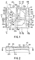
- a power detecting element 20 according to the first embodiment of the present invention will be described below with reference to FIGS. 1 to 8.
- this power detecting element 20 is formed on a rectangular insulating sapphire substrate 21 about 1 mm in side length and about 20 ⁇ m (micrometers) thick.
- a sapphire substrate having small dielectric loss and high thermal conductivity is used as the insulating substrate 21.
- a thin-film member 22 made from micro-crystalline silicon germanium is formed from the center of one surface 21a of the substrate 21 to a side 21b.
- This thin-film member 22 has a thickness of approximately 1 ⁇ m and is composed of a resistor 22a and first, second, and third extending portions 22b, 22c, and 22d.
- the first extending portion 22b runs from one end of the resistor 22a to the center of the side 21b of the substrate 21.
- the second extending portion 22c runs from the other end of the resistor 22a to the corner between the side 21b and a side 21c of the substrate 21.
- the third extending portion 22d connects with the second extending portion 22c and runs from the other end of the resistor 22a to the corner between the side 21b and a side 21d of the substrate 21.
- the first extending portion 22b is axially symmetrical with a line connecting the center of the substrate 21 to the center of the side 21b. Also, a width Wa of this first extending portion 22b in a direction along the side 21b of the substrate 21 monotonically increases in a direction from one end of the resistor 22a to the side 21b of the substrate 21.
- a width Wb of the second and third extending portions 22c and 22d in the direction along the side 21b of the substrate 21 and a distance Ga from these second and third extending portions 22c and 22d to the first extending portion 22b increase in direct proportion to the width Wa of the first extending portion 22b.
- an input connecting portion 23 having the same external shape as the first extending portion 22b and made of a thin-film metal is formed to overlap the first extending portion 22b.
- ground (GND) connecting portions 24 and 25 having the same external shapes as the second and third extending portions 22c and 22d, respectively, and made of a thin-film metal are formed to overlap the second and third extending portions 22c and 22d, respectively.
- ground connecting portions 24 and 25 communicate with each other at the other end of the resistor 22a.
- These connecting portions 23, 24, and 25 are made of a low-resistance metal film (or a plurality of stacked layers of thin films of different metals) of, e.g., platinum or gold, having a thickness of about 0.5 ⁇ m.
- An input electrode 26 and ground (GND) electrodes 27 and 28, each having a wide rectangular shape, are formed on end portions 23a, 24a, and 25a of the connecting portions 23, 24, and 25, respectively, on the side 21b of the substrate 21.
- These electrodes 26, 27, and 28 are made of a gold-plated layer about 5 ⁇ m thick.
- the electrodes 26, 27, and 28 are connected to the two ends of the resistor 22a via the connecting portions 23, 24, and 25, respectively.
- the resistance of the resistor 22c which forms a thin-film resistor by connecting its two ends to the input connecting portion 23 and the ground connecting portions 24 and 25, is determined by the material of the thin-film member 22 and the width, length, and thickness of the resistor 22a.
- the area of the resistor 22a is decreased so that heat generating portions of the power detecting element 20 are concentrated into one point in the center of the substrate 21, and that the resistor 22a is a pure resistor up to a RF region. Also, the dimensions of individual portions are so set that the resistance is 50 ⁇ (or 75 ⁇ ) which is equal to the transmission impedance of a RF coaxial cable.
- the input electrode 26 and the ground electrodes 27 and 28 are so formed as to have large areas in order to ensure the easiness of packaging.
- the connecting portions 23, 24, and 25 connecting with the input electrode 26 and the ground electrodes 27 and 28 widen toward the side 21b of the substrate 21 and communicate with the electrodes 26, 27, and 28.
- the ratio of the width Wa of the input connecting portion 23 and the input electrode 26 to the gap Ga between the ground connecting portions 24 and 25 and the ground electrodes 27 and 28 is held substantially constant. Consequently, the impedance viewed from the input terminal is substantially equal to the resistance of the resistor 22a.
- the transmission impedance of a coplanar transmission line is determined substantially in accordance with the value of (W + G)/W and the line length.
- the transmission line length is short. Therefore, the width of the input connecting portion 23 and the gap between the ground connecting portions 24 and 25 are linearly increased, and the ratio of the width Wa to the gap Ga is fixed.
- this power detecting element 20 broadens to 65 GHz or more, which is twice the aforesaid conventional frequency or more.
- thermocouples 30 and 35 are formed on a side 21e of the substrate 21 away from the resistor 22a with the ground connecting portions 24 and 25 between them.
- the thermocouple 30 has a thin-film member 31 formed into a substantially rectangular shape long from end to end on one surface 21a of the substrate 21.
- thermocouple 35 has a thin-film member 36 formed into a substantially rectangular shape long from side to side on one surface 21a of the substrate 21.
- These thin-film members 31 and 36 are made of a micro-crystalline silicon germanium thin film having the same thickness as the thin-film member 22 forming the resistor 22a.
- corners 31a and 36a of the thin-film members 31 and 36 are close to the resistor 22a, and diagonal corners 31b and 36b are far from the resistor 22a.
- one end 32a of a first output connecting portion 32 is connected to overlap the corner 31a of the thin-film member 31.
- This connecting portion is a hot junction of the thermocouple 30.
- the first output connecting portion 32 so runs as to surround the perimeter of the thin-film member 31.
- thermocouple 30 The other end 32b of this first output connecting portion 32 forms a cold junction of the thermocouple 30 and runs to the corner between the two sides 21c and 21e of the substrate 21.
- One end 33a of an intermediate connecting portion 33 is connected to overlap the corner 31b of the thin-film member 31 in wide area.
- This connecting portion forms a cold junction of the thermocouples 30 and 35.
- the other end 33b of the intermediate connecting portion 33 is connected to overlap the corner 36a of the thin-film member 36.
- This connecting portion forms a hot junction of the thermocouple 35.
- a second output connecting portion 37 serving as a cold junction of the thermocouple 36 is connected to overlap the corner 36b of the thin-film member 36.
- the first and second output connecting portions 32 and 37 and the intermediate connecting portion 33 are made of a low-resistance metal thin film, similar to the input connecting portion 23 and the ground connecting portions 24 and 25.
- output electrodes 38 and 39 having a rectangular shape long from end to end and made of a gold-plated layer about 5 ⁇ m thick are formed at the same level as the input electrode 26 and the ground electrodes 27 and 28.
- a thin-film member 34 made from micro-crystalline silicon germanium is formed into a rectangular shape long from end to end, in order to level the surface of the end 32b of the first output connecting portion 32 with the surface of the second output connecting portion 37.
- thermocouples 30 and 35 This heat raises the temperature at a hot junction Hj of the two thermocouples 30 and 35. Consequently, these two thermocouples 30 and 35 generate electromotive forces V directly proportional to a temperature difference ⁇ T between the hot junction Hj and a cold junction Cj.
- micro-crystalline silicon germanium forming the thin-film members 22, 31, 34, and 36 has a Seebeck coefficient, which represents the magnitude of electromotive force corresponding to the temperature difference between a hot junction and a cold junction, of 100 to 200 ⁇ V/K.
- This value is about an order of magnitude larger than those of conventional metal thin-film materials.
- micro-crystalline silicon germanium forming the thin-film members 22, 31, 34, and 36 has dependence of conductivity on temperature far smaller than those of other micro-crystalline semiconductor thin films. Therefore, as described above, this micro-crystalline silicon germanium can be used as the resistor 22a for converting a signal into heat and as one thermocouple material of each of the two thermocouples 30 and 35.
- micro-crystalline silicon germanium is stable at a high temperature of 600°C and hence is immune to burning out even when large power to be measured is supplied to the resistor 22a.
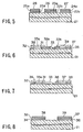
- Steps of manufacturing this power detecting element 20 are as described in (a) to (d) below.
- the resistor 22a and one thermocouple material of each thermocouple are formed by the same micro-crystalline silicon germanium thin film. Additionally, the connecting portions and electrodes formed on this micro-crystalline silicon germanium thin film are formed by the same metal thin film, resulting in simple manufacturing steps. Accordingly, it is possible to inexpensively manufacture the power detecting elements 20 for wide-band RF signals, which have high yield and uniform characteristics.
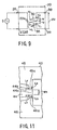
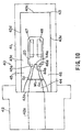
- the power detecting element 20 manufactured in this way is incorporated, as it is mounted on a module substrate 43, into a case 41 of a power detecting device 40, as shown in FIG. 10.
- This case 41 is made of a metal in order to thermally shield the exterior and the interior, and is formed into, e.g., a cylindrical shape.
- a coaxial connector 42 for connecting a coaxial cable (not shown) is formed in one end of this case 41.
- the module substrate 43 guides a signal to be measured input from the coaxial connector 42 to the power detecting element 20 and externally outputs an output signal from the power detecting element 20.
- This module substrate 43 has the shape of a rectangle.
- a central conductor 44 is formed by patterning from an end 43b to an end 43c of a surface 43a of the module substrate 43.
- This central conductor 44 connects a core 42a of the coaxial connector 42 to the input electrode 26 of the power detecting element 20.
- the central conductor 44 is so formed as to decrease its thickness in a direction from the end 43b to the end 43c of the module substrate 43.
- This mount portion 44a has an elongated portion 44b which is elongated, with the same width Wb, by a predetermined distance Lc toward one end 40b of the module substrate 43.
- Ground (GND) conductors 45 and 46 are formed on the two sides of the central conductor 44 by patterning.
- ground conductors 45 and 46 form a coplanar transmission line together with the central conductor 44.
- the ratio of a width Wc of the central conductor 44 to a gap Gc from the central conductor 44 to the ground conductors 45 and 46 is held substantially constant.
- ground conductors 45 and 46 that are on the two sides of the mount portion 44a of the central conductor 44 have rectangular mount portions 45a and 46a, respectively, matching the ground (GND) electrodes 27 and 28 of the power detecting elements 20.
- ground conductors 45 and 46 connect with each other in the rear portion of the module substrate 43 and are in contact with the case 41 in two side portions 43d and 43e of the module substrate 43.
- the elongated portion 44b of the central conductor 44 prevents disturbance of the impedance, caused by an increase in the capacitance between the junction portion of the input electrode 26 of the power detecting element 20 and the mount portion 44a and the junction portions of the ground electrodes 27 and 28 of the power detecting element 20 and the mount portions 45a and 46a, when the power detecting element 20 is mounted on the module substrate 43.
- the ratio of the width Wc of the central conductor 44 to the gap Gc between the central conductor 44 and the ground conductors 45 and 46 is changed (made smaller than the width determined by the ratio) only in this portion. This gives the central conductor 44 inductance corresponding to the capacitance increase, thereby preventing disturbance to the impedance resulting from the capacitance increase.
- a pair of output conductors 47 and 48 are formed parallel by patterning.
- the spacing and width of these output conductors 47 and 48 are substantially equal to the spacing and width of the output electrodes 38 and 39 of the power detecting element 20.
- the power detecting element 20 is soldered to the module substrate 43 constructed as above, with the surface 21a of the substrate 21 facing the surface 43a of the module substrate 43, the input electrode 26 and the ground electrodes 27 and 28 overlapping the mount portions 44a, 45a, and 46a of the module substrate 43, and the output electrodes 38 and 39 overlapping the output conductors 47 and 48.
- an amplifier e.g., a chopper amplifier for amplifying output signals from the output conductors 47 and 48 is formed at the end 43c of the module substrate 43.
- thermocouples a series output of the electromotive forces of the two thermocouples is amplified by this amplifier and output to the outside of the case 41.
- An indicator or the like indicates the power of this signal.
- FIG. 12 shows the measurement results of the frequency vs. sensitivity characteristics of this power detecting device 40 and the conventional device described previously.
- a curve A in FIG. 12 indicates the characteristic of the power detecting device 40 with reference to the output when direct current is input.
- a curve B in FIG. 12 indicates the characteristic of the conventional device.
- a curve C in FIG. 12 indicates the characteristic when the central conductor 44 of the module substrate 43 has no elongated portion 44b.
- the sensitivity lowers by 1 dB at substantially 40 GHz.
- FIG. 13 shows the measurement result of the frequency-to-voltage standing wave ratio of the power detecting device 40.
- the SWR (Standing Wave Ratio) of the power detecting device 40 of this embodiment is decreased to 1.5 or less from DC to 65 GHz, so this power detecting device 40 can accurately detect power, over this wide band, without being largely influenced by reflecting waves.
- one thin-film resistor absorbs the power of a signal to be measured.
- a plurality of thin-film transistors can also absorb the power of a signal to be measured.
- a power detecting element 20' shown in FIG. 14 has two thin-film transistors 22a' and 22a' on a substrate 21.
- One end of each of these two thin-film transistors 22a' and 22a' is connected to an input connecting portion 23.
- the other end of one thin-film transistor 22a' is connected to the distal end of a ground connecting portion 24.
- the other end of the other thin-film resistor 22a' is connected to the distal end of a ground connecting portion 25.
- each thin-film resistor 22a' is substantially twice that of the resistor 22a in the first embodiment, this resistance can be matched with the transmission impedance viewed from an input electrode 26 and ground electrodes 27 and 28.
- ground connecting portions can also be connected to each other on the substrate 21.
- the number of thin-film resistors is not limited to two and can be further increased.
- the power of a signal to be measured is divisionally absorbed by these resistors. This disperses the heat generation, increases the burnout level of each resistor, and improves the heat resistance.
- thermocouples are separated from thermocouples, so the pattern of these input resistors can be formed independently of the thermocouples. Accordingly, even if the number of thin-film transistors is increased, the frequency characteristic does not deteriorate.
- the power detecting element 20 of the first embodiment has two thermocouples. However, only one thermocouple can also be used if the sensitivity is of no great importance.
- the sensitivity of the power detecting element 20 of the first embodiment can be further increased by using three thermocouples.
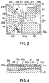
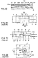
- FIGS. 15 to 19 show a power detecting element 50 having seven thermocouples according to this third embodiment.
- a resistor 52a and first, second, and third extending portions 52b, 52c, and 52d are formed by a thin-film member 52 made from micro-crystalline silicon germanium.
- An input connecting portion 53 is formed to overlap the first extending portion 52b.
- Ground (GND) connecting portions 54 and 55 are formed to overlap the second and third extending portions 52c and 52d, respectively.
- the input connecting portion 53 is so formed as to widen toward a side 51b of the substrate 51.
- An input electrode 56 made of a gold-plated layer is formed in an end portion 53a of this input connecting portion 53.
- ground connecting portions 54 and 55 communicate with each other at the other end of the resistor 52a. These ground connecting portions 54 and 55 run to the corner between the side 51b and a side 51c of the substrate 51 and to the corner between the side 51b and a side 51d, respectively.
- Ground electrodes 57 and 58 made of a gold-plated layer are formed in end portions 54a and 55a of the ground connecting portions 54 and 55, respectively.
- the input connecting portion 53 and the input electrode 56, and the ground connecting portions 54 and 55 and the ground electrodes 57 and 58 are formed so that the ratio of the width of the input connecting portion 53 and the input electrode 56 to the gap between the ground connecting portions 54 and 55 and the ground electrodes 57 and 58 is held substantially constant, and so as to form a coplanar transmission line having transmission impedance substantially equal to the resistance of the resistor 52a.
- thermocouples 61 to 67 radially arrayed as shown in FIG. 15 are formed on the surface of the substrate 51 away from the ground connecting portions 54 and 55 with the resistor 52a between them.
- thermocouples 61 to 67 have substantially fan-shaped thin-film members 71 to 77, respectively, which divide the range from the ground connecting portions 54 and 55 to a side 51e of the substrate 51 into seven segments.
- These thin-film members 71 to 77 are made from micro-crystalline silicon germanium. As shown in FIG. 18, on the surfaces of these thin-film members 71 to 77, insulating films 81 to 87 are formed except for distal end portions 71a to 77a close to the resistor 52a and outer edge portions 71b to 77b outside a circle of a predetermined radius centering around the resistor 52a.
- a thin-film member 78 for receiving one output electrode is formed between the perimeter of the thin-film member 71 adjacent to the ground connecting portion 54 and the corner between the two sides 51c and 51e of the substrate 51.
- a thin-film member 79 for receiving the other output electrode runs between the outer edge of the thin-film member 77 adjacent to the ground connecting portion 55 and the corner between the two sides 51d and 51e of the substrate 51.
- Insulating films 88a to 88c are formed between intermediate portions, between the input connecting portion 53 and the ground connecting portions 54 and 55, and the thin-film member 52.
- One end 91a of an output connecting portion 91 is connected to the distal end portion 71a of the thin-film member 71, adjacent to the ground connecting portion 54, so as to overlap this end portion 71a.
- This connecting portion forms a hot junction of the thermocouple 61.
- the output connecting portion 91 extends from the distal end portion 71a of the thin-film member 71 to the corner between the two sides 51c and 51e of the substrate 51, over the insulating film 81, so as to overlap the thin-film member 78.
- One end 92a of an intermediate connecting portion 92 is connected to overlap the outer edge portion 71b of the thin-film member 71 in wide area.
- This intermediate connecting portion 92 runs from the outer edge portion 71b of the thin-film member 71 to the distal end portion 72a of the thin-film member 72, over the insulating film 81 and the insulating film 82 of the adjacent thin-film member 72.
- the other end 92b of the intermediate connecting portion 92 is connected to the distal end portion 72a of the thin-film member 72.
- portions between the thin-film members 72 to 77 are connected via intermediate connecting portions 93 to 97, respectively.
- the outer edge portion 77b of the thin-film member 77 is connected to an output connecting portion 98 so formed as to overlap the thin-film member 79.
- Output electrodes 99 and 100 made of a gold-plated layer are formed at the same level in the end portions of the output connecting portions 91 and 97.
- thermocouples 61 to 67 the sum of the electromotive forces of the seven thermocouples 61 to 67 is output between the output electrodes 99 and 100.
- the input electrode 56, the ground electrodes 57 and 58, and the resistor 52a are connected by the coplanar transmission line so that the transmission impedance is substantially equal to the resistance of the resistor 52a.
- this power detecting element 50 has a frequency characteristic exceeding 65 GHz, like the power detecting element 20 of the first embodiment.
- the input connecting portion and the ground connecting portions overlap in a broad range of the thin-film member forming the resistor.
- a thin-film member as a resistor only in a limited range on one surface of a substrate and form connecting portions so that their end portions overlap the two ends of this resistor, thereby connecting these connecting portions to an input electrode and ground electrodes.
- an elongated portion 44b narrower than a predetermined width determined by the transmission impedance is formed to connect with the mount portion of a central conductor 44, thereby increasing the inductance in accordance with the capacitance increase.
- the inductance corresponding to the capacitance increase can also be formed in a position separated from the mount portion of the central conductor 44.
- the central conductor 44 is set, over its whole length, to a predetermined width determined by the transmission impedance, a notch or the like is formed in a ground conductor 45 so as to partially widen the gap between the central conductor 44 and the ground conductor 45. In this manner, the central conductor 44 can be given an inductance corresponding to the capacitance increase caused by mounting of the power detecting element.
- FIGS. 23A and 23B show a coaxial type wide-band RF signal power detecting device (coaxial power sensor) according to the fourth embodiment of the present invention.
- a module substrate 111 on which, as shown in FIG. 23A, a wide-band RF signal power detecting element (power sensor element) 110, formed in the same manner as in the first to third embodiments described above, is mounted is incorporated, as shown in FIG. 23B, into a coaxial module tube 114 as a coaxial case, thereby realizing a coaxial type wide-band RF signal power detecting device (coaxial power sensor) 113.
- Reference numeral 112 in FIG. 23A denotes solder for cementing used to mount the power detecting element (power sensor element) 110 on the module substrate 111.
- Reference numeral 115 in FIG. 23B denotes a contact portion that projects into the front end portion of the coaxial module tube 114 as a coaxial case incorporating the module substrate 111.
- Reference numeral 116 in FIG. 23B denotes a hollow portion (absorber) of the coaxial module tube 114 as a coaxial case incorporating the module substrate 111.
- Reference numeral 117 in FIG. 23B denotes a lead line that projects from the rear end portion of the coaxial module tube 114 as a coaxial case incorporating the module substrate 111.
- Reference numeral 118 in FIG. 23B denotes a cover attached to the coaxial module tube 114 as a coaxial case incorporating the module substrate 111.
- this coaxial power sensor 113 comprises the coaxial module tube 114 which transmits a RF signal supplied, via a coaxial cable (not shown), from a RF signal source to the contact portion 115, which projects into the front end portion of the coaxial module tube 114, of the module substrate 111, the module substrate 111 formed inside this coaxial module tube 114, and the power sensor element 110 formed on this module substrate 111.
- a RF signal to be measured supplied from the coaxial cable (not shown) is transmitted to the module substrate 111 via the contact portion 115 for matching conversion to a microstrip line of a coplanar structure.
- the RF signal to be measured is converted from a coaxial-mode electromagnetic wave, propagating in the coaxial cable, into a coplanar-mode electromagnetic wave.
- the coplanar-mode RF signal thus converted propagates in the vicinity of the surface of a dielectric material sandwiched between a signal line of a central conductor, as a microstrip line, on the module substrate 111 and an external ground conductor. After that, this RF signal is absorbed by the resistor of the power sensor element 110 mounted on the module substrate 111 and thereby converted into heat.
- the magnitude of the generation of heat by this conversion is directly proportional to the magnitude of the power of the supplied RF signal to be measured.
- the magnitude of the heat generation is converted into DC voltage by using a thermocouple placed close to the resistor of the power sensor element 110.
- This DC voltage is supplied to a dedicated meter (not shown) via the lead line 117, and the magnitude of the voltage is displayed.
- the contact portion 115 is formed on a surface in the center of the module substrate 111 and perpendicular to the longitudinal direction of the module substrate 111.
- This contact portion 115 is desirably made of a thin-film piece, which has high electrical conductivity and is soft, such as a gold ribbon, in order to improve the contact with a coaxial cable terminal (not shown).
- the material of the coaxial module tube 114 is desirably, e.g., copper or brass, having high electrical conductivity.
- plastic having a small linear expansion coefficient as a base material and to cover the surface with plating of an electrically, thermally conductive material, such as gold or nickel.
- the coplanar module substrate 111 sapphire or aluminum having a large dielectric constant and a small dielectric loss is used.
- solder fusing method which uses the solder 112 to mount the power detecting element (power sensor element) 110 on the module substrate 111 as described earlier is used.
- the hollow portion 116 of the coaxial module tube 114 is desirably filled with an electromagnetic wave absorber, such as polyiron, in order to increase the measurement accuracy.
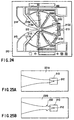
- FIGS. 24 to 27 show a waveguide type wide-band RF signal power detecting element (power sensor element) and a waveguide type wide-band RF signal power detecting apparatus using the element.
- Coaxial type and waveguide type elements are possible as millimeter-wave power sensor elements.
- a coaxial type power detecting element (power sensor element) and a coaxial type power detecting device using the same is realized in each of the first to fourth embodiments described above.
- a waveguide type power detecting element (power sensor element) and a waveguide type power detecting device using the same can be realized by this fifth embodiment.
- the structure of a waveguide type power detecting element is basically the same as the coaxial type element except that the waveguide type element has two input terminals.
- the common feature of the coaxial type and waveguide type elements is that impedance mismatching is compensated for by using a geometrical shape, thereby obtaining desired performance (FIGS. 25A and 25B).
- FIG. 24 relates to the structure of a waveguide type power detecting element (power sensor element) 210 and is particularly a plan view showing an element chip.
- the chip size of this element is 0.9 mm square.
- thermocouples 213 are formed to surround this resistor 212, by using thin film deposition and lithography.
- thermocouples 213 include seven thermocouples 213a to 213g formed in the same manner as the seven thermocouples 61 to 67 of the power detecting element 50 according to the third embodiment shown in FIGS. 15 to 19.
- This waveguide type power detecting element (power sensor element) 210 has tapered electrodes 214 and 215 to suppress reflection of incident millimeter-wave power.
- each taper is 0.4 mm, and its exit opening (facing the resistor 212) is 0.03 mm.
- tapered electrodes 214 and 215 are formed to suppress reflection of incident millimeter-wave power, in practice a large impedance change is readily produced by this abrupt taper. In effect, large reflection having a reflectance of 0.13 takes place.
- the incident portion of this resistor 212 has a predetermined inclination angle (20 to 90°, desirably, 45 to 90°) to the axial line.
- reflection having a reflectance of about 0.2 still occurs.
- This embodiment is characterized in that the abovementioned two reflectances (RF1) can be substantially canceled in relation to a module substrate for mounting the waveguide type power detecting element (power sensor element) 210 as shown in FIG. 24.
- FIGS. 25A and 25B are schematic views in which the waveguide type power detecting element (power sensor element) 210 as shown in FIG. 24 is mounted on the fin line module substrate 231a and 231b used to match with the waveguide.
- the material of these fin line module substrates 231a and 231b is alumina, and their thickness is 0.05 to 0.1 mm.
- the fin line module substrates 231a and 231b have fin line electrodes for exponentially changing the impedance, in order to smoothly match with the impedance of the waveguide.
- the entrance opening of the fin line electrode is substantially level with the waveguide, and its exit opening is 0.4 mm, meeting the taper of the waveguide type power detecting element 210.
- FIG. 25A shows the fin line module substrate 231a having no recess for compensation in the fin line electrode.
- FIG. 25B shows the fin line module substrate 231b having a recess for compensation in the fin line electrode.
- the fin line module substrate 231a or 231b shown in FIG. 25B has a recess 232 formed in a portion close to the waveguide type power detecting element (power sensor element) 210, with this waveguide type power detecting element (power sensor element) 210 mounted.
- the fin line module substrate 231a or 231b shown in FIG. 25B produces reflection with reflectance RF2 at the two end faces of the recess 232 owing to changes in the impedance, with the waveguide type power detecting element (power sensor element) 210 mounted.
- the absolute value of the reflection with the reflectance RF1 produced in the waveguide type power detecting element (power sensor element) 210 and the absolute value of the reflection with the reflectance RF2 produced in the fin line module substrate 231b can be set to be substantially equal to each other, and the phase difference can be set to 180°.
- the reflection with the reflectance RF1 produced in the waveguide type power detecting element (power sensor element) 210 can be canceled by the reflection with the reflectance RF2 produced in the fin line module substrate 231b.
- FIGS. 26A and 26B show the measurement results of an SWR in the V band (50 to 75 GHz) and the X band (75 to 110 Hz), respectively, of the waveguide type power detecting device constructed as above.
- the SWR produced in this waveguide type power detecting device with compensation indicated by the solid line is smaller than that produced without compensation indicated by the broken line. That is, in either case the performance greatly improved.
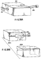
- FIG. 27 is a view showing the way the waveguide type power detecting device constructed as above is packaged.
- the fin line module substrate 231b mounting the waveguide type power detecting element (power sensor element) 210 is packaged as it is sandwiched between waveguide cases 233a and 233b, split into two parts as casings.
- an input terminal (WR15 flange) 234 for millimeter-wave signals is formed in the front portion, and sensor output terminals (two DC terminals) 236 are formed in the rear portion.
- a BNC coaxial input terminal 237 for inputting a calibration signal is formed on one side.
- the casings for the two, V and W, bands have the same outer dimensions, and the dimensions of their inner waveguides are (3.76 ⁇ 1.88 mm) and (2.54 ⁇ 1.27 mm), respectively.
- FIGS. 28A and 28B show a waveguide type wide-band RF signal power detecting device (power sensor) according to the sixth embodiment of the present invention.
- the waveguide type wide-band RF signal power detecting element (power sensor element) 254 As a waveguide type wide-band RF signal power detecting element (power sensor element) 254, the waveguide type wide-band RF signal power detecting element (power sensor element) realized in the fifth embodiment described above is used.
- the power sensor of this embodiment comprises a waveguide connector 251, a module casing 252, a fin line module 253, the power sensor element 254, and a lead line 255.
- the waveguide connector 251 connects a waveguide (not shown) to the power sensor to guide a signal to be measured propagating in the waveguide to the power sensor.
- the module casing 252 has a waveguide-shaped hollow portion capable of propagating a signal to be measured.
- the fin line module substrate 253 is formed in a portion of the waveguide-shaped hollow portion in the module casing 252 and is analogous to that in the fifth embodiment.
- the power sensor element 254 is formed on this fin line module substrate 253.
- the lead line 255 guides an output signal from this power sensor element 254 to a dedicated meter.
- a signal to be measured propagating in the waveguide propagates in the waveguide-shaped hollow portion of the module casing 252, propagates in a fin line electrode formed on the fin line module substrate 253, and is concentrated to be narrowed to the center of this fin line electrode.
- the RF signal to be measured thus concentrated to the center of the fin line electrode is absorbed by a resistor of the power sensor element 254 mounted on the fin line module substrate 253 and converted into heat.
- the magnitude of the generation of heat by the conversion is directly proportional to the magnitude of the power of the supplied RF signal to be measured.
- the magnitude of the heat generation is converted into DC voltage by using a thermocouple placed close to the resistor.
- This DC voltage is supplied to the dedicated meter via the lead line and displayed to indicate the magnitude of the power of the RF signal to be measured.
- a connector (not shown) for supplying a calibration signal (DC or 1-MHz RF signal) is formed in a portion of the module casing 252.
- the fin line module substrate 253 is placed parallel to the longitudinal direction of the waveguide-shaped hollow portion.
- a signal to be measured propagates in the TE mode in the waveguide.
- the fin line module substrate 253 placed in the waveguide-shaped hollow portion of the module casing 252 is set parallel to the longitudinal direction of the waveguide-shaped hollow portion and perpendicular to the longitudinal direction of the section of the hollow portion, in order to minimize reflected waves.
- this fin line module substrate 253 To increase the detection sensitivity it is important for this fin line module substrate 253 to maximize a signal supplied from a signal to be measured propagating in the waveguide-shaped hollow portion of the module casing 252.
- the fin line module substrate 253 is placed parallel to the longitudinal direction of the waveguide-shaped hollow portion of the module casing 252 and perpendicular to the longitudinal direction of the section of the hollow portion. Additionally, the fin line module substrate 253 is positioned in 1/3 portions of the distances from the centers in the longitudinal directions.
- this module casing is desirably constructed of two complementary waveguide casings 252a and 252b.
- the height of projections on the surfaces of the inner walls of the waveguide-shaped hollow portion of the module casing 252 is desirably very small, e.g., 3 ⁇ m or less.
- the material of this module casing 252 is desirably copper or brass having high electrical thermal conductivity. However, it is also effective, to decrease the cost, to use plastic having a small linear expansion coefficient as a base material and to cover the surface with plating of an electrically, thermally conductive material, such as gold or nickel.
- the fin line module substrate 253 sapphire or aluminum having a large dielectric constant and a small dielectric loss is used.
- solder fusing method As a method of mounting the power sensor element on this fin line module substrate 253, a solder fusing method is used.
- a thin-film absorber or an electromagnetic wave absorber such as polyiron, is desirably placed, or charged, behind the power sensor element, in order to increase the accuracy with which the signal is measured.
- heat generated in the resistor can be efficiently conducted to the thermocouple when the substrate or the module substrate is made of a high-heat-conductivity material.
- thermocouple To efficiently conduct heat generated in the resistor to the thermocouple, a high-heat-conductivity material can also be interposed between the resistor and the thermocouple.
- one end of a thin-film resistor formed on an insulating substrate is connected to an input electrode formed at one end of the substrate.
- the other end of this thin-film resistor is connected to a ground electrode formed at the same end of the substrate.
- a thin-film thermocouple is formed in the vicinity of the thin-film resistor to form a indirect heating structure in which the resistor and the thermocouple are separated. The transmission impedance between a first connecting portion connecting with the input electrode and connecting the input electrode to the thin-film resistor and a second connecting portion connecting with the ground electrode and connecting the ground electrode to the thin-film resistor is held at a predetermined value.
- the size of the thin-film resistor can be decreased independently of the thermocouple. Additionally, the upper limit of the measurement frequency can be greatly increased because the transmission impedance viewed from the input electrode and the ground electrode can be well approached to the resistance of the thin-film resistor.
- the thin-film resistor is made smaller than the input electrode and the ground electrode, and the first connecting portion is widened toward the input electrode. This facilitates mounting the power detecting element.
- the ground electrode and the second connecting portion are so formed as to sandwich the input electrode and the first connecting portion. This allows the use of a coplanar transmission line. Also, since matching can be easily obtained with respect to the resistance of the thin-film resistor small in size, the upper limit of the measurement frequency can be greatly increased.
- the fourth power detecting element of the present invention has two thin-film resistors. This improves the heat resistance and allows measurements of large power.
- the fifth power detecting element of the present invention has a structure in which all members are formed using thin films on the substrate. Since this allows easy manufacture, it is possible to provide elements having uniform characteristics inexpensively.
- a coplanar transmission line is formed by making the ratio of the width of the input electrode and the first connecting portion to the gap between the ground electrode and the second connecting portion substantially constant. Accordingly, the transmission impedance between the input electrode and first connecting portion and the ground electrode and second connecting portion can be easily matched with the resistance of the thin-film resistor. Consequently, the upper limit of the measurement frequency can be greatly increased.
- the thin film resistor and one member of the thermocouple are made of a microcrystalline silicon germanium thin film. This further facilitates the manufacture, stabilizes the operation, and raises the burnout level. Therefore, highly accurate power detection can be performed.
- thermocouples are radially arranged around the thin-film resistor on one surface of the substrate, and these thermocouples are connected in series. Accordingly, a large number of thermocouples can be formed in the limited substrate area, and micro watt power can be measured.
- the transmission impedance of a central conductor and a ground conductor for guiding a signal to be measured to a power detecting element mounted on a module substrate is made substantially equal to the transmission impedance between electrodes of the power detecting element.
- the central conductor is given an inductance component corresponding to a capacitance component increased by junctions between mounting portions and the electrodes of the power detecting element. It is, therefore, possible to cancel the capacitance increased by the junctions between the mounting portions and the electrodes of the power detecting element.
- a signal to be measured guided by the central conductor and the ground conductor can be input to a resistor of the power detecting element in a matched state over a broad frequency range. So, the frequency characteristic of the power detecting element can be well brought out, and the upper-limit detection frequency of the whole device can be greatly extended.
- the present invention includes the following forms as a coaxial type wide-band RF signal power detecting element (power sensor element), a waveguide type wide-band RF signal power detecting element (power sensor), and a power detecting device using the same.
- the present invention can provide a wide-band RF signal power detecting element which is easy to manufacture, has a high upper-limit detection frequency, can detect power from direct current, and has a frequency characteristic not influenced by the number of thermocouples.
- the present invention can also provide a power detecting device using a wide-band RF power detecting element which is easy to manufacture, has a high upper-limit detection frequency, can detect power from direct current, and has a frequency characteristic not influenced by the number of thermocouples.
Applications Claiming Priority (1)
| Application Number | Priority Date | Filing Date | Title |
|---|---|---|---|
| PCT/JP1998/002364 WO1999061926A1 (fr) | 1998-05-28 | 1998-05-28 | Element de detection de puissance de signal haute frequence a large bande, et detecteur utilisant un tel element |
Publications (2)
| Publication Number | Publication Date |
|---|---|
| EP1004883A1 true EP1004883A1 (de) | 2000-05-31 |
| EP1004883A4 EP1004883A4 (de) | 2001-10-04 |
Family
ID=14208286
Family Applications (1)
| Application Number | Title | Priority Date | Filing Date |
|---|---|---|---|
| EP98921866A Withdrawn EP1004883A4 (de) | 1998-05-28 | 1998-05-28 | Breitbandiges hochfrequenz-leistungsdetektionselement und leistungsdetektor unter vewendung eines solchen elements |
Country Status (3)
| Country | Link |
|---|---|
| US (2) | US6518743B1 (de) |
| EP (1) | EP1004883A4 (de) |
| WO (1) | WO1999061926A1 (de) |
Cited By (3)
| Publication number | Priority date | Publication date | Assignee | Title |
|---|---|---|---|---|
| GB2374942A (en) * | 2001-04-26 | 2002-10-30 | Marconi Caswell Ltd | RF sensor using Seebeck effect |
| DE102008057607A1 (de) * | 2008-11-17 | 2010-05-27 | Rohde & Schwarz Gmbh & Co. Kg | Thermoelektrische Leistungsmesszelle und entsprechendes Messverfahren |
| WO2011110255A3 (de) * | 2010-03-11 | 2012-01-05 | Rohde & Schwarz Gmbh & Co. Kg | Messspitze mit integriertem messwandler |
Families Citing this family (11)
| Publication number | Priority date | Publication date | Assignee | Title |
|---|---|---|---|---|
| KR100465235B1 (ko) * | 2002-04-16 | 2005-01-13 | 삼성전자주식회사 | 정전용량에 의해 rf 신호에 대한 전력을 측정하는 rf파워센서 |
| US6931333B2 (en) * | 2002-05-17 | 2005-08-16 | Bookham Technology Plc | Electrical power sensing |
| US6753807B1 (en) * | 2002-07-30 | 2004-06-22 | The United States Of America As Represented By The Secretary Of Commerce | Combination N-way power divider/combiner and noninvasive reflected power detection |
| US7670045B2 (en) * | 2004-06-18 | 2010-03-02 | Raytheon Company | Microstrip power sensor |
| US7095294B2 (en) * | 2004-06-30 | 2006-08-22 | Agilent Technologies, Inc. | Directional bridge coupler |
| JP2006258667A (ja) * | 2005-03-17 | 2006-09-28 | Nec Electronics Corp | パッケージ基板のrfインピーダンス測定装置 |
| US7372249B2 (en) * | 2006-01-31 | 2008-05-13 | Agilent Technologies, Inc. | Load measurement for a thermal microwave power sensor |
| US10145938B2 (en) | 2014-04-26 | 2018-12-04 | Infineon Technologies Ag | Power sensor for integrated circuits |
| JP6488720B2 (ja) * | 2015-01-23 | 2019-03-27 | 三菱電機株式会社 | 半導体装置 |
| US10180458B2 (en) | 2015-05-14 | 2019-01-15 | Rohde & Schwarz Gmbh & Co. Kg | Measuring system and measuring method with power calibration |
| EP3912175A4 (de) * | 2019-01-15 | 2022-10-12 | Smiths Interconnect Americas, Inc. | Hochfrequenz-spiralabschluss |
Citations (3)
| Publication number | Priority date | Publication date | Assignee | Title |
|---|---|---|---|---|
| DD256628A (de) * | ||||
| GB1090613A (en) * | 1963-10-21 | 1967-11-08 | Marconi Instruments Ltd | Improvements in or relating to electrical power meters |
| US4733170A (en) * | 1985-05-28 | 1988-03-22 | Marconi Instruments Limited | Microwave power sensors |
Family Cites Families (11)
| Publication number | Priority date | Publication date | Assignee | Title |
|---|---|---|---|---|
| DE256628C (de) | ||||
| US2314764A (en) * | 1941-04-26 | 1943-03-23 | Rca Corp | Ultra high frequency wattmeter |
| US2782377A (en) * | 1951-06-29 | 1957-02-19 | Myron C Selby | Micropotentiometers |
| US2995708A (en) * | 1959-11-09 | 1961-08-08 | Paul A Hudson | Dry static calorimeter for rf power measurement |
| US3447083A (en) * | 1966-12-01 | 1969-05-27 | Marconi Instruments Ltd | Electrical power metering device for insertion in a transmission line |
| JPS5597574U (de) * | 1978-12-26 | 1980-07-07 | ||
| JPS5597574A (en) | 1979-01-17 | 1980-07-24 | Babcock Hitachi Kk | Safety valve drip pan device |
| DD219296A1 (de) * | 1983-10-28 | 1985-02-27 | Robotron Elektronik | Mikrowellenleistungsmesser |
| EP0289618B1 (de) | 1986-10-24 | 1993-03-10 | Anritsu Corporation | Mit einem dünnschichtleiter versehener elektrischer widerstand und kraftsensor |
| US4943764A (en) * | 1987-12-11 | 1990-07-24 | Hewlett-Packard Company | Wide dynamic range radio-frequency power sensor |
| JP3029707B2 (ja) | 1991-07-17 | 2000-04-04 | 株式会社日本触媒 | 硬化性樹脂組成物 |
-
1998
- 1998-05-28 US US09/462,653 patent/US6518743B1/en not_active Expired - Fee Related
- 1998-05-28 EP EP98921866A patent/EP1004883A4/de not_active Withdrawn
- 1998-05-28 WO PCT/JP1998/002364 patent/WO1999061926A1/ja not_active Application Discontinuation
-
2002
- 2002-12-06 US US10/313,448 patent/US6741070B2/en not_active Expired - Fee Related
Patent Citations (3)
| Publication number | Priority date | Publication date | Assignee | Title |
|---|---|---|---|---|
| DD256628A (de) * | ||||
| GB1090613A (en) * | 1963-10-21 | 1967-11-08 | Marconi Instruments Ltd | Improvements in or relating to electrical power meters |
| US4733170A (en) * | 1985-05-28 | 1988-03-22 | Marconi Instruments Limited | Microwave power sensors |
Non-Patent Citations (1)
| Title |
|---|
| See also references of WO9961926A1 * |
Cited By (7)
| Publication number | Priority date | Publication date | Assignee | Title |
|---|---|---|---|---|
| GB2374942A (en) * | 2001-04-26 | 2002-10-30 | Marconi Caswell Ltd | RF sensor using Seebeck effect |
| GB2374942B (en) * | 2001-04-26 | 2004-07-28 | Marconi Caswell Ltd | Electrical power sensing |
| DE102008057607A1 (de) * | 2008-11-17 | 2010-05-27 | Rohde & Schwarz Gmbh & Co. Kg | Thermoelektrische Leistungsmesszelle und entsprechendes Messverfahren |
| US9194895B2 (en) | 2008-11-17 | 2015-11-24 | Rohde & Schwarz Gmbh & Co. Kg | Thermoelectric power measurement cell and corresponding measurement method |
| DE102008057607B4 (de) | 2008-11-17 | 2022-01-13 | Rohde & Schwarz GmbH & Co. Kommanditgesellschaft | Thermoelektrische Leistungsmesszelle und entsprechendes Messverfahren |
| WO2011110255A3 (de) * | 2010-03-11 | 2012-01-05 | Rohde & Schwarz Gmbh & Co. Kg | Messspitze mit integriertem messwandler |
| US9081035B2 (en) | 2010-03-11 | 2015-07-14 | Rohde & Schwarz Gmbh & Co. Kg | Test probe with integrated test transformer |
Also Published As
| Publication number | Publication date |
|---|---|
| US20030080725A1 (en) | 2003-05-01 |
| WO1999061926A1 (fr) | 1999-12-02 |
| EP1004883A4 (de) | 2001-10-04 |
| US6518743B1 (en) | 2003-02-11 |
| US6741070B2 (en) | 2004-05-25 |
Similar Documents
| Publication | Publication Date | Title |
|---|---|---|
| EP1004883A1 (de) | Breitbandiges hochfrequenz-leistungsdetektionselement und leistungsdetektor unter vewendung eines solchen elements | |
| JP5227327B2 (ja) | 集積型テラヘルツアンテナおよび送信機および/または受信機ならびにその製造方法 | |
| US7705582B2 (en) | Broadband micro-machined thermal power sensor | |
| JP5151032B2 (ja) | 磁界プローブ装置及び磁界プローブ素子 | |
| EP0320265B1 (de) | Hochfrequenz-Leistungssensor mit grossem dynamischen Bereich | |
| US6759839B2 (en) | Wide-band RF signal power detecting element and power detecting device using the same | |
| US20030214309A1 (en) | RF power sensor for measuring an RF signal power using capacitance | |
| US4963195A (en) | Electric resistor and a power detector both comprising a thin film conductor | |
| US6767129B2 (en) | Microwave power sensor and method for manufacturing the same | |
| NL2000793C2 (nl) | Probe voor het meten van een elektrisch veld. | |
| Peterson et al. | A CPW T-resonator technique for electrical characterization of microwave substrates | |
| US6812800B2 (en) | Atomic oscillator | |
| Yassin et al. | A 350-GHz SIS antipodal finline mixer | |
| EP0645001B1 (de) | Verwendung von vanadium oxyd in mikrobolometer sensoren | |
| US7482814B2 (en) | Electric/magnetic field sensor | |
| US6239587B1 (en) | Probe for monitoring radio frequency voltage and current | |
| JP2008064653A (ja) | スペクトロメータ | |
| US10044320B2 (en) | Robust waveguide millimeter wave noise source | |
| JP2010088011A (ja) | 方向性結合器 | |
| JP3496179B2 (ja) | 電力検出素子および電力検出装置 | |
| CN111896131A (zh) | 基于微带天线的温度传感器及系统 | |
| Wuensch et al. | Investigation and optimization of LEKID coupling structures and multi-pixel arrays at 4.2 K | |
| CN112526221A (zh) | 电磁场复合探头和探测系统 | |
| Kadi et al. | Printed dipoles antennas for MCM-L wireless RF interconnects | |
| Shireen | Design and characterization of modules for millimeter-wave imaging applications |
Legal Events
| Date | Code | Title | Description |
|---|---|---|---|
| PUAI | Public reference made under article 153(3) epc to a published international application that has entered the european phase |
Free format text: ORIGINAL CODE: 0009012 |
|
| 17P | Request for examination filed |
Effective date: 20000216 |
|
| AK | Designated contracting states |
Kind code of ref document: A1 Designated state(s): DE FR GB |
|
| A4 | Supplementary search report drawn up and despatched |
Effective date: 20010820 |
|
| AK | Designated contracting states |
Kind code of ref document: A4 Designated state(s): DE FR GB |
|
| STAA | Information on the status of an ep patent application or granted ep patent |
Free format text: STATUS: THE APPLICATION HAS BEEN WITHDRAWN |
|
| 18W | Application withdrawn |
Effective date: 20070424 |