EP0982869A1 - Telecommunication device - Google Patents
Telecommunication device Download PDFInfo
- Publication number
- EP0982869A1 EP0982869A1 EP97949153A EP97949153A EP0982869A1 EP 0982869 A1 EP0982869 A1 EP 0982869A1 EP 97949153 A EP97949153 A EP 97949153A EP 97949153 A EP97949153 A EP 97949153A EP 0982869 A1 EP0982869 A1 EP 0982869A1
- Authority
- EP
- European Patent Office
- Prior art keywords
- circuit
- signal
- tuning
- interrogator
- demodulating
- Prior art date
- Legal status (The legal status is an assumption and is not a legal conclusion. Google has not performed a legal analysis and makes no representation as to the accuracy of the status listed.)
- Granted
Links
Images

Classifications
-
- H—ELECTRICITY
- H04—ELECTRIC COMMUNICATION TECHNIQUE
- H04B—TRANSMISSION
- H04B1/00—Details of transmission systems, not covered by a single one of groups H04B3/00 - H04B13/00; Details of transmission systems not characterised by the medium used for transmission
- H04B1/59—Responders; Transponders
-
- G—PHYSICS
- G06—COMPUTING OR CALCULATING; COUNTING
- G06K—GRAPHICAL DATA READING; PRESENTATION OF DATA; RECORD CARRIERS; HANDLING RECORD CARRIERS
- G06K19/00—Record carriers for use with machines and with at least a part designed to carry digital markings
- G06K19/06—Record carriers for use with machines and with at least a part designed to carry digital markings characterised by the kind of the digital marking, e.g. shape, nature, code
- G06K19/067—Record carriers with conductive marks, printed circuits or semiconductor circuit elements, e.g. credit or identity cards also with resonating or responding marks without active components
- G06K19/07—Record carriers with conductive marks, printed circuits or semiconductor circuit elements, e.g. credit or identity cards also with resonating or responding marks without active components with integrated circuit chips
- G06K19/0723—Record carriers with conductive marks, printed circuits or semiconductor circuit elements, e.g. credit or identity cards also with resonating or responding marks without active components with integrated circuit chips the record carrier comprising an arrangement for non-contact communication, e.g. wireless communication circuits on transponder cards, non-contact smart cards or RFIDs
Definitions
- the present invention relates to a data communication apparatus which receives a radio wave transmitted from an antenna to generate power for communication.
- a high frequency tag which generates power by a radio wave transmitted from an antenna and transmits information which has been stored therein, has been developed and used for a gate of the ski lift, gate at the station, sorting of parcels and the like.
- the high frequency tag is provided with a non-volatile memory and a transmission/reception mechanism, but not with a power supply source such as a battery.
- a power supply source such as a battery.
- power is generated by the received radio wave (a high frequency signal).
- the power supply source needs not be provided therein and information exchange can be performed for a long period of time.
- remote (non-contact) data communication can advantageously be performed as it is performed by the radio wave.
- one type of radio wave one-wave mode
- two types of radio waves two-wave mode
- an interrogator Only one type of carrier with information is transmitted from the responder in a one-wave mode, so that the carrier is rectified to generate power and also detected to obtain information.
- a first carrier for generation of power which has not been modulated and a second carrier with information are transmitted.
- the first and second carriers are separately received, so that the first carrier is rectified to generate power and the second carrier is detected to obtain information.
- responders used in these modes are of course different in structure
- the responder used in one mode cannot be used in the other mode. Therefore, two types of responders are required to perform communication in both modes. Accordingly, two types of integrated circuits (IC) forming the responders must be manufactured. This disadvantageously results not only in increase in the designing, manufacturing and product cost, but also in complicated management of the products (integrated circuit, communication apparatus and the like) for proper use.
- IC integrated circuits
- An object of the present invention is to provide a data communication apparatus (a responder) which can be used both in one-wave and two-wave modes.
- a data communication apparatus for data communication with an interrogator including: a power generating circuit generating power by a signal having a first frequency transmitted from the interrogator; and a modulating circuit modulating the signal having the first frequency in accordance with response information for an interrogation data when the signal having the first frequency transmitted from the interrogator has been modulated in accordance with the interrogation data, and modulating a signal having a second frequency in accordance with response information for an interrogation data obtained by demodulating the signal having the second frequency transmitted from the interrogator when the signal having the first frequency transmitted form the interrogator has not been modulated.
- An advantage of the present invention is that one data communication apparatus (responder) enables communication both in the one-wave mode and two-wave mode, so that two types of data communication apparatuses are not necessary.
- two types of integrated circuits forming the data communication apparatuses needs not be manufactured, reduction in the designing, manufacturing and product cost is achieved and management of the products (integrated circuits or communication apparatuses) for proper use is facilitated.
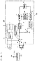
- Fig. 1 is a block diagram showing an overall structure of a high frequency tag (a responder) according to a first embodiment of the present invention.
- a high frequency tag 100 receives and transmits a signal from and to an interrogator 200 having an antenna 201 by a radio wave, and is provided with a first tuning circuit 1, a second tuning circuit 2 and an integrated circuit 110.
- first tuning circuit 1 includes a tuning coil L1 tuning approximately to 13.56 MHz and functioning as a reception antenna, and a tuning condenser C1 connected between both ends of tuning coil L1.
- a signal having a tuned frequency f 1 which is determined by tuning coil L1 and tuning condenser C1 is output from tuning coil L1.
- Second tuning circuit 2 includes a tuning coil L2 tuning approximately to 3.39 MHz and functioning as a transmission/reception antenna, and a tuning condenser C2 connected between both ends of tuning coil L2.
- a signal having a tuned frequency f 2 which is determined by tuning coil L2 and tuning condenser C2 is output from tuning coil L2.
- integrated circuit 110 includes: a power supply circuit 3 connected to first tuning circuit 1 and generating power by the received high frequency signal; an information processing circuit 15; and a switching circuit 6 which is formed of a semiconductor switch and connected to a connecting point A in the initial state.
- Power supply circuit 3 includes a rectifying circuit 4 rectifying a tuned signal and a regulator 5 connected to rectifying circuit 4 and stabilizing a voltage rectified by and transmitted from rectifying circuit 4. It is noted that an output voltage of regulator 5 is supplied for each circuit in integrated circuit 110.
- information processing circuit 15 includes: a detection circuit 7 connected to switching circuit 6 and detecting (demodulating) a modulated signal (a carrier) shown in Fig. 8A which is supplied from first tuning circuit 1 or second tuning circuit 2 for obtaining an information signal shown in Fig. 8B; and a decoder 8 connected to detection circuit 7.
- the information signal shown in Fig. 8B is a digital signal, which is shaped to be a pulse signal having a waveform in a rectangular shape by a waveform shaping circuit (not shown) and then supplied for decoder 8.
- decoder 8 decodes the above mentioned pulse signal in accordance with a prescribed protocol and outputs a digital data. It is noted that, generally, decoder 8 also performs serial-parallel conversion.
- Information processing circuit 15 includes a memory 12 connected to decoder 8. Memory 12 is accessed by an address designation data output from decoder 8 and, a data stored at the designated address is read.
- Information processing circuit 15 includes: an encoder 10 connected to memory 12; a protocol supplying portion 9 connected to decoder 8 and encoder 10; a pulsating circuit 11 connected to encoder 10; and an N channel MOS transistor 13 having its gate connected to pulsating circuit 11.
- an encoding process is performed for the data which is read from memory 12 by encoder 10 in accordance with the protocol supplied from protocol supplying portion 9.
- encoder 10 also performs parallel-serial conversion.
- the data which has been converted to serial data is in turn converted to a pulse train signal by pulsating circuit 11 and supplied for the gate of N channel MOS transistor 13.
- Information processing circuit 15 includes a signal transmission line 16 connecting switching circuit 6 and detection circuit 7, and the N channel MOS transistor has its source connected to a round node and its drain connected to signal transmission line path 16. In the periods in which N channel MOS transistor 13 is turned on and off, an impedance of first tuning circuit 1 or second tuning circuit 2 which is connected to signal transmission line 16 via switching circuit 6 is different.
- Information processing circuit 15 includes a switch control circuit 14 connected to detection circuit 7 and detecting a mode of the received radio wave for selectively connecting a connecting point A or connecting point B by switching circuit 6.
- Switch control circuit 14 checks an output signal from first tuning circuit 1 and, if the output signal is related to the one-wave mode, connects connecting point A by switching circuit 6, but connects connecting point B by switching circuit 6 if the output signal is related to the two-wave mode. It is noted that connecting point A is connected by switching circuit 6 in the initial state and the output signal from first tuning circuit 1 is detected by detection circuit 7.
- Switch control circuit 14 includes a latch circuit 32, a register 33 and a comparator 34 connected to latch circuit 32 and register 33 as shown for example in Fig. 7.
- latch circuit 32 latches a prescribed number of bits of the output signal from detection circuit 7, and register 33 stores a reference data for the one-wave mode (or two-wave mode).
- Comparator 34 compares an output signal from latch circuit 32 and an output signal from register 33 and, continues to output "1" if they match, but "0" if they mismatch. For example, if register 33 stores the data related to the one-wave mode, connecting point A is connected by switching circuit 6 when "1" is output, whereas connecting point B is connected by switching circuit 6 when "0" is output.
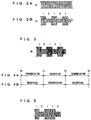
- a first signal of a carrier which has not been modulated and which has a frequency f 1 shown in Fig. 2A and a second signal which is an arbitrary information signal such as "10101" shown in Fig. 2B and a carrier having an amplitude-modulated frequency f 2 are transmitted from antenna 201.
- first tuning circuit 1 receives the first signal and second tuning circuit 2 receives the second signal.
- the received first signal is converted to power by power supply circuit 3, so that the power is supplied for every circuit in high frequency tag 100 including detection circuit 7, switch control circuit 14 and the like as operating power.
- the first signal received by first tuning circuit 1 is supplied for detection circuit 7 via switching circuit 6 as connecting point A is connected by switching circuit 6 in the initial state, and the two-wave mode of interrogator 200 is detected by switch control circuit 14.
- connecting point B is connected by switching circuit 6, and the second signal received by second tuning circuit 2 is supplied for information processing circuit 15 by signal transmission line 16.
- information "10101" from the second signal shown in Fig. 2B is decoded by decoder 8, and response information " 10110" for the information shown in Fig. 5 is pulsated by pulsating circuit 11.
- N channel MOS transistor 13 is turned on/off in accordance with the pulse train signal which has been pulsated by pulsating circuit 11, and the impedance of second tuning circuit 2 is changed.
- transmission periods T0-T1, T2-T3 and reception period T1-T2 are alternately arranged as shown in Fig. 4A for interrogator 200.
- a modulated signal such as the one shown in Fig. 2B is transmitted in transmission periods T0-T1, T2-T3, for example, a signal of a carrier at frequency f 2 , which has not been modulated, is transmitted in reception period T1-T2.
- reception period T1-T2 since the impedance of second tuning circuit 2 which is to be a load of interrogator 200 is changed in accordance with on/off of N channel MOS transistor 13 by the radio wave, a signal which has been amplitude-modulated in accordance with "10110" shown in Fig.
- Fig. 4B is a timing chart showing the operation of high frequency tag 100. As shown in Fig. 4B, the operation of high frequency tag 100 is in a reverse relation with respect to the operation of interrogator 200 shown in Fig. 4A.
- a mode of high frequency tag 100 is switched between transmission and reception modes by a command, which is transmitted from interrogator 200 as a part of information.
- interrogator 200 When interrogator 200 has the one-wave mode, only a signal of a carrier having a frequency f 0 which has been amplitude-modulated for example by the information as shown in Fig. 3 is supplied for high frequency tag 100.
- frequency f 0 is the same as or close to frequency f 1 of a signal including a carrier for the two-wave mode.
- the signal shown in Fig. 3 is received by first tuning circuit 1.
- no signal is received by second tuning circuit 2, so that an output therefrom would be 0.
- the signal received by first tuning circuit 1 is converted to power by power supply circuit 3. Unlike the case of the two-wave mode, although there is a slight variation in an output voltage level of rectifying circuit 4 for rectifying the modulated signal, the voltage is kept at a prescribed level by regulator 5.
- the received signal is also detected by detection circuit 7 through switching circuit 6, and connecting point A is still connected by switching circuit 6 as the one-wave mode is detected by switch control circuit 14.
- N channel MOS transistor 13 is turned on/off by the pulse train signal output from pulsating circuit 11, and the impedance of first tuning circuit 1 is changed.
- transmission of the response information to interrogator 200 is performed by the radio wave received by first tuning circuit 1.
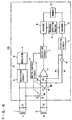
- Fig. 6 is a block diagram showing an overall structure of a high frequency tag (a responder) according to a second embodiment of the present invention.
- the high frequency tag has a structure which is similar to that of the high frequency tag according to the first embodiment, except that one end of second tuning circuit 2 is not connected to a ground node, signal transmission lines 16a and 16b are respectively connected through switching circuits 6a and 6b to both ends of second tuning circuit 2, and the high frequency tag is provided with a comparator 17 having input ends connected to signal transmission lines 16a and 16b, an inverter 18 and a resistance R1 which are connected in series between pulsating circuit 11 and signal transmission line 16a and a resistance R2 connected between pulsating circuit 11 and signal transmission line 16b, where switch control circuit 14 controls switching circuit 6a and switching circuit 6b.
- switch control circuit 14 makes switching circuits 6a and 6b connect connecting points on the same side. In other words, when connecting point A is connected by switching circuit 6a, for example, connecting point A is also connected by switching circuit 6b.
- High frequency tag 101 having such structure also enables data communication with interrogator 200 both in the one-wave mode and two-wave mode as in the case of high frequency tag 100 according to the above described first embodiment.
Landscapes
- Engineering & Computer Science (AREA)
- Computer Networks & Wireless Communication (AREA)
- Theoretical Computer Science (AREA)
- Microelectronics & Electronic Packaging (AREA)
- Physics & Mathematics (AREA)
- General Physics & Mathematics (AREA)
- Computer Hardware Design (AREA)
- Signal Processing (AREA)
- Near-Field Transmission Systems (AREA)
- Radar Systems Or Details Thereof (AREA)
- Circuits Of Receivers In General (AREA)
- Transmitters (AREA)
- Transceivers (AREA)
Abstract
Description
Claims (3)
- A data communication apparatus for data communication with an interrogator (200), comprising:power generating means (3) for generating power by a signal having a first frequency transmitted from said interrogator (200); andmodulating means (1, 2, 6, 15) for modulating said signal having the first frequency in accordance with response information for an interrogation data when said signal having the first frequency transmitted from said interrogator (200) has been modulated in accordance with said interrogation data and for modulating a signal having a second frequency in accordance with the response information for an interrogation data obtained by demodulating said signal having the second frequency transmitted from said interrogator (200) when said signal having the first frequency transmitted from said interrogator (200) has not been modulated.
- The data communication apparatus according to claim 1, wherein said modulating means (1, 2, 6, 15) includes:first tuning means (1) for transmitting and receiving said signal having the first frequency;second tuning means (2) for transmitting and receiving said signal having the second frequency;demodulating means (7) for demodulating a signal received by one of said first tuning means and said second tuning means;switching means (6, 6a, 6b) for connecting said demodulating means and one of said first tuning means and said second tuning means and for connecting said demodulating means and said first tuning means in an initial state; andswitch controlling means (14) connected to said demodulating means for controlling said switching means to connect said demodulating means and said first tuning means when said signal having the first frequency demodulated by said demodulating means has been modulated and to connect said demodulating means and said second tuning means when said signal has not been modulated.
- The data communication apparatus according to claim 2, wherein said modulating means (15) further includes differential amplifying means (17) connected between said switching means (6a, 6b) and said demodulating means (7) for differentially inputting the signal received by said first tuning means (1) or said second tuning means (2).
Applications Claiming Priority (3)
| Application Number | Priority Date | Filing Date | Title |
|---|---|---|---|
| JP7692297 | 1997-03-28 | ||
| JP07692297A JP3916291B2 (en) | 1997-03-28 | 1997-03-28 | Information communication equipment |
| PCT/JP1997/004693 WO1998044649A1 (en) | 1997-03-28 | 1997-12-18 | Telecommunication device |
Publications (3)
| Publication Number | Publication Date |
|---|---|
| EP0982869A1 true EP0982869A1 (en) | 2000-03-01 |
| EP0982869A4 EP0982869A4 (en) | 2000-03-08 |
| EP0982869B1 EP0982869B1 (en) | 2002-05-08 |
Family
ID=13619211
Family Applications (1)
| Application Number | Title | Priority Date | Filing Date |
|---|---|---|---|
| EP97949153A Expired - Lifetime EP0982869B1 (en) | 1997-03-28 | 1997-12-18 | Telecommunication device |
Country Status (9)
| Country | Link |
|---|---|
| US (1) | US6498923B2 (en) |
| EP (1) | EP0982869B1 (en) |
| JP (1) | JP3916291B2 (en) |
| KR (1) | KR100306306B1 (en) |
| CN (1) | CN1247651A (en) |
| AU (1) | AU8949398A (en) |
| CA (1) | CA2283250C (en) |
| DE (1) | DE69712531T2 (en) |
| WO (1) | WO1998044649A1 (en) |
Cited By (4)
| Publication number | Priority date | Publication date | Assignee | Title |
|---|---|---|---|---|
| WO2000045328A1 (en) * | 1999-01-26 | 2000-08-03 | Koninklijke Philips Electronics N.V. | Data carrier provided with at least two decoding stages |
| WO2002091290A1 (en) * | 2001-05-03 | 2002-11-14 | Ip And Innovation Company Holdings (Proprietary) Limited | Communication between a transponder and an interrogator |
| EP2367262A4 (en) * | 2008-12-12 | 2014-04-02 | Hanrim Postech Co Ltd | CONTACTLESS ENERGY RECEIVING DEVICE AND JIG FOR PRODUCING A CORE FOR THIS RECEIVING DEVICE |
| EP3258424A4 (en) * | 2015-02-11 | 2018-06-27 | Tendyron Corporation | Electronic equipment |
Families Citing this family (25)
| Publication number | Priority date | Publication date | Assignee | Title |
|---|---|---|---|---|
| TW463399B (en) * | 1999-03-19 | 2001-11-11 | Seiko Epson Corp | Electronic device |
| US7049935B1 (en) | 1999-07-20 | 2006-05-23 | Stmicroelectronics S.A. | Sizing of an electromagnetic transponder system for a dedicated distant coupling operation |
| FR2796781A1 (en) | 1999-07-20 | 2001-01-26 | St Microelectronics Sa | DIMENSIONING OF AN ELECTROMAGNETIC TRANSPONDER SYSTEM FOR HYPERPROXIMITY OPERATION |
| FR2804557B1 (en) * | 2000-01-31 | 2003-06-27 | St Microelectronics Sa | ADAPTING THE TRANSMISSION POWER OF AN ELECTROMAGNETIC TRANSPONDER DRIVE |
| FR2808946A1 (en) * | 2000-05-12 | 2001-11-16 | St Microelectronics Sa | VALIDATION OF THE PRESENCE OF AN ELECTROMAGNETIC TRANSPONDER IN THE FIELD OF A READER |
| FR2808945B1 (en) * | 2000-05-12 | 2002-08-16 | St Microelectronics Sa | EVALUATION OF THE NUMBER OF ELECTROMAGNETIC TRANSPONDERS IN THE FIELD OF A READER |
| FR2808941B1 (en) * | 2000-05-12 | 2002-08-16 | St Microelectronics Sa | VALIDATION OF THE PRESENCE OF AN ELECTROMAGNETIC TRANSPONDER IN THE FIELD OF AN AMPLITUDE DEMODULATION READER |
| FR2808942B1 (en) * | 2000-05-12 | 2002-08-16 | St Microelectronics Sa | VALIDATION OF THE PRESENCE OF AN ELECTROMAGNETIC TRANSPONDER IN THE FIELD OF A PHASE DEMODULATION READER |
| FR2809235A1 (en) * | 2000-05-17 | 2001-11-23 | St Microelectronics Sa | ANTENNA FOR GENERATING AN ELECTROMAGNETIC FIELD FOR TRANSPONDER |
| FR2809251B1 (en) * | 2000-05-17 | 2003-08-15 | St Microelectronics Sa | DEVICE FOR PRODUCING AN ELECTROMAGNETIC FIELD FOR A TRANSPONDER |
| US7103344B2 (en) * | 2000-06-08 | 2006-09-05 | Menard Raymond J | Device with passive receiver |
| FR2812986B1 (en) | 2000-08-09 | 2002-10-31 | St Microelectronics Sa | DETECTION OF AN ELECTRIC SIGNATURE OF AN ELECTROMAGNETIC TRANSPONDER |
| US20030169169A1 (en) | 2000-08-17 | 2003-09-11 | Luc Wuidart | Antenna generating an electromagnetic field for transponder |
| DE10258779A1 (en) * | 2002-12-16 | 2004-07-15 | Infineon Technologies Ag | Method for contactless data transmission and use of this method |
| US20040192379A1 (en) * | 2003-03-27 | 2004-09-30 | Industrial Technology Research Institute | Method and apparatus for transmitting signals of a battery-free cordless microphone |
| US7183917B2 (en) * | 2003-05-19 | 2007-02-27 | Checkpoint Systems, Inc. | EAS/RFID identification hard tags |
| EP1920571B1 (en) * | 2005-08-11 | 2013-01-23 | Semiconductor Energy Laboratory Co., Ltd. | Semiconductor device and wireless communication system |
| JP2007143116A (en) * | 2005-10-19 | 2007-06-07 | Seiko Epson Corp | Wireless communication device |
| KR100662615B1 (en) * | 2006-01-13 | 2007-01-02 | 삼성전자주식회사 | Signal converter, driving method of RDF tag and RDF tag having same |
| WO2008016527A2 (en) * | 2006-07-29 | 2008-02-07 | Powercast Corporation | Rf power transmission network and method |
| WO2008035296A2 (en) * | 2006-09-22 | 2008-03-27 | Koninklijke Philips Electronics N.V. | Extended functionality of rfid devices |
| US9106269B2 (en) * | 2010-12-08 | 2015-08-11 | Access Business Group International Llc | System and method for providing communications in a wireless power supply |
| CN103647576B (en) * | 2013-12-20 | 2015-12-02 | 大同裕隆环保有限责任公司 | The data transmit-receive module of Intelligent charging frame |
| CN106571692B (en) * | 2015-10-09 | 2019-06-04 | 纽艾吉科技有限公司 | Wireless receiving device and its demodulation method |
| US11527138B2 (en) | 2018-05-17 | 2022-12-13 | Checkpoint Systems, Inc. | Dual hard tag |
Family Cites Families (14)
| Publication number | Priority date | Publication date | Assignee | Title |
|---|---|---|---|---|
| US3839717A (en) * | 1972-01-28 | 1974-10-01 | Identification Co Inc | Communication apparatus for communicating between a first and a second object |
| US4114151A (en) * | 1976-09-14 | 1978-09-12 | Alfa-Laval Company Limited | Passive transponder apparatus for use in an interrogator-responder system |
| JPS60171475A (en) * | 1984-02-15 | 1985-09-04 | アイデンティフィケ−ション・デバイセス・インコ−ポレ−テッド | Discriminating system |
| FR2578126B1 (en) * | 1985-02-26 | 1992-01-03 | Lecheviller Jean Pierre | TELEPHONE APPARATUS WITH FIXED TERMINAL AND MOBILE HANDSET |
| JPH02249319A (en) * | 1989-03-22 | 1990-10-05 | Tokyo Keiki Co Ltd | Data communication system |
| JPH0683551B2 (en) * | 1989-06-02 | 1994-10-19 | 山武ハネウエル株式会社 | Wireless receiver |
| ATE135835T1 (en) | 1990-07-16 | 1996-04-15 | Siemens Ag | DEVICE FOR CONTACTLESS DATA AND ENERGY TRANSMISSION AND USE OF SUCH |
| AT395224B (en) * | 1990-08-23 | 1992-10-27 | Mikron Ges Fuer Integrierte Mi | CONTACTLESS, INDUCTIVE DATA TRANSFER SYSTEM |
| JPH0779296B2 (en) | 1990-10-17 | 1995-08-23 | 三菱電機株式会社 | Non-contact type portable carrier |
| DE59304677D1 (en) * | 1993-03-24 | 1997-01-16 | Siemens Ag | Device and method for wireless data and energy transmission |
| US5602744A (en) * | 1994-09-29 | 1997-02-11 | Meek; Jean L. | Universal send/receive utility usage data gathering system |
| JP3800634B2 (en) | 1994-12-20 | 2006-07-26 | 松下電工株式会社 | Non-contact identification system |
| US5649295A (en) * | 1995-06-19 | 1997-07-15 | Lucent Technologies Inc. | Dual mode modulated backscatter system |
| US5842118A (en) * | 1996-12-18 | 1998-11-24 | Micron Communications, Inc. | Communication system including diversity antenna queuing |
-
1997
- 1997-03-28 JP JP07692297A patent/JP3916291B2/en not_active Expired - Fee Related
- 1997-12-18 EP EP97949153A patent/EP0982869B1/en not_active Expired - Lifetime
- 1997-12-18 CN CN97181955A patent/CN1247651A/en active Pending
- 1997-12-18 WO PCT/JP1997/004693 patent/WO1998044649A1/en not_active Ceased
- 1997-12-18 CA CA002283250A patent/CA2283250C/en not_active Expired - Fee Related
- 1997-12-18 AU AU89493/98A patent/AU8949398A/en not_active Abandoned
- 1997-12-18 DE DE69712531T patent/DE69712531T2/en not_active Expired - Fee Related
- 1997-12-18 US US09/355,989 patent/US6498923B2/en not_active Expired - Lifetime
-
1999
- 1999-08-20 KR KR1019997007563A patent/KR100306306B1/en not_active Expired - Fee Related
Cited By (9)
| Publication number | Priority date | Publication date | Assignee | Title |
|---|---|---|---|---|
| WO2000045328A1 (en) * | 1999-01-26 | 2000-08-03 | Koninklijke Philips Electronics N.V. | Data carrier provided with at least two decoding stages |
| WO2002091290A1 (en) * | 2001-05-03 | 2002-11-14 | Ip And Innovation Company Holdings (Proprietary) Limited | Communication between a transponder and an interrogator |
| EP2367262A4 (en) * | 2008-12-12 | 2014-04-02 | Hanrim Postech Co Ltd | CONTACTLESS ENERGY RECEIVING DEVICE AND JIG FOR PRODUCING A CORE FOR THIS RECEIVING DEVICE |
| US10804745B2 (en) | 2008-12-12 | 2020-10-13 | Ge Hybrid Technologies, Llc | Non-contact power reception apparatus for non-contact charging and electronic settlement performed in a single portable terminal |
| US10992184B2 (en) | 2008-12-12 | 2021-04-27 | Ge Hybrid Technologies, Llc | Non-contact power reception apparatus for non-contact charging and electronic settlement performed in a single portable terminal |
| US11095163B2 (en) | 2008-12-12 | 2021-08-17 | Ge Hybrid Technologies, Llc | Non-contact power reception apparatus for non-contact charging and electronic settlement performed in a single portable terminal |
| US11601014B2 (en) | 2008-12-12 | 2023-03-07 | Ge Hybrid Technologies, Llc | Non-contact power reception apparatus for non-contact charging and electronic settlement performed in a single portable terminal |
| US12388296B2 (en) | 2008-12-12 | 2025-08-12 | Ge Hybrid Technologies, Llc | Non-contact power reception apparatus for non-contact charging and electronic settlement performed in a single portable terminal |
| EP3258424A4 (en) * | 2015-02-11 | 2018-06-27 | Tendyron Corporation | Electronic equipment |
Also Published As
| Publication number | Publication date |
|---|---|
| EP0982869B1 (en) | 2002-05-08 |
| KR100306306B1 (en) | 2001-11-03 |
| EP0982869A4 (en) | 2000-03-08 |
| CN1247651A (en) | 2000-03-15 |
| WO1998044649A1 (en) | 1998-10-08 |
| CA2283250C (en) | 2002-04-30 |
| US20020137463A1 (en) | 2002-09-26 |
| KR20000075504A (en) | 2000-12-15 |
| AU8949398A (en) | 1998-10-22 |
| JP3916291B2 (en) | 2007-05-16 |
| US6498923B2 (en) | 2002-12-24 |
| DE69712531T2 (en) | 2002-11-07 |
| JPH10276114A (en) | 1998-10-13 |
| DE69712531D1 (en) | 2002-06-13 |
| CA2283250A1 (en) | 1998-10-08 |
Similar Documents
| Publication | Publication Date | Title |
|---|---|---|
| EP0982869B1 (en) | Telecommunication device | |
| US7173519B2 (en) | Circuit arrangement with simplified input circuit for phase modulation in a backscattering transponder | |
| US5729236A (en) | Identification system reader with multiplexed antennas | |
| EP1026832B1 (en) | Information communication device | |
| KR0142673B1 (en) | Data transmitter | |
| CA1272787A (en) | Transponder useful in a system for identifying objects | |
| USRE44415E1 (en) | Wireless communication medium and method for operating the same | |
| US7215249B2 (en) | Radio frequency identification reader | |
| US6654466B1 (en) | Data communication equipment, data communication system, and data communication method | |
| EP1314134B1 (en) | Identification transponder | |
| DK1099188T3 (en) | Improved reading device for contactless labels | |
| US5305469A (en) | Modem for telecommunication system with a reflection amplifier function | |
| JP4336379B2 (en) | RFID carrier sense method and RFID system using the same | |
| JP5107777B2 (en) | Receiving device, reader / writer, and RFID system | |
| KR100737855B1 (en) | Single Side Band Response Method of Wireless Identification Tag | |
| US5191345A (en) | Circuit to increase the information bit rate in a system for the exchange of data | |
| JP3851009B2 (en) | Data carrier | |
| JPH0918381A (en) | RFID system | |
| US20040051627A1 (en) | Modulator for electromagnetic signals transmitted by a contactless transmission/reception system | |
| JPH0453131B2 (en) |
Legal Events
| Date | Code | Title | Description |
|---|---|---|---|
| PUAI | Public reference made under article 153(3) epc to a published international application that has entered the european phase |
Free format text: ORIGINAL CODE: 0009012 |
|
| 17P | Request for examination filed |
Effective date: 19990818 |
|
| AK | Designated contracting states |
Kind code of ref document: A1 Designated state(s): DE FR GB NL |
|
| A4 | Supplementary search report drawn up and despatched |
Effective date: 20000120 |
|
| AK | Designated contracting states |
Kind code of ref document: A4 Designated state(s): DE FR GB NL |
|
| RIC1 | Information provided on ipc code assigned before grant |
Free format text: 7H 04B 1/59 A, 7G 06K 19/07 B |
|
| 17Q | First examination report despatched |
Effective date: 20000915 |
|
| GRAG | Despatch of communication of intention to grant |
Free format text: ORIGINAL CODE: EPIDOS AGRA |
|
| GRAG | Despatch of communication of intention to grant |
Free format text: ORIGINAL CODE: EPIDOS AGRA |
|
| GRAH | Despatch of communication of intention to grant a patent |
Free format text: ORIGINAL CODE: EPIDOS IGRA |
|
| REG | Reference to a national code |
Ref country code: GB Ref legal event code: IF02 |
|
| GRAH | Despatch of communication of intention to grant a patent |
Free format text: ORIGINAL CODE: EPIDOS IGRA |
|
| GRAA | (expected) grant |
Free format text: ORIGINAL CODE: 0009210 |
|
| AK | Designated contracting states |
Kind code of ref document: B1 Designated state(s): DE FR GB NL |
|
| REF | Corresponds to: |
Ref document number: 69712531 Country of ref document: DE Date of ref document: 20020613 |
|
| PG25 | Lapsed in a contracting state [announced via postgrant information from national office to epo] |
Ref country code: GB Free format text: LAPSE BECAUSE OF NON-PAYMENT OF DUE FEES Effective date: 20021218 |
|
| PLBE | No opposition filed within time limit |
Free format text: ORIGINAL CODE: 0009261 |
|
| STAA | Information on the status of an ep patent application or granted ep patent |
Free format text: STATUS: NO OPPOSITION FILED WITHIN TIME LIMIT |
|
| 26N | No opposition filed |
Effective date: 20030211 |
|
| PG25 | Lapsed in a contracting state [announced via postgrant information from national office to epo] |
Ref country code: NL Free format text: LAPSE BECAUSE OF NON-PAYMENT OF DUE FEES Effective date: 20030701 |
|
| GBPC | Gb: european patent ceased through non-payment of renewal fee |
Effective date: 20021218 |
|
| NLV4 | Nl: lapsed or anulled due to non-payment of the annual fee |
Effective date: 20030701 |
|
| PGFP | Annual fee paid to national office [announced via postgrant information from national office to epo] |
Ref country code: FR Payment date: 20081212 Year of fee payment: 12 |
|
| PGFP | Annual fee paid to national office [announced via postgrant information from national office to epo] |
Ref country code: DE Payment date: 20081211 Year of fee payment: 12 |
|
| REG | Reference to a national code |
Ref country code: FR Ref legal event code: ST Effective date: 20100831 |
|
| PG25 | Lapsed in a contracting state [announced via postgrant information from national office to epo] |
Ref country code: FR Free format text: LAPSE BECAUSE OF NON-PAYMENT OF DUE FEES Effective date: 20091231 |
|
| PG25 | Lapsed in a contracting state [announced via postgrant information from national office to epo] |
Ref country code: DE Free format text: LAPSE BECAUSE OF NON-PAYMENT OF DUE FEES Effective date: 20100701 |