EP0981843B1 - Laser devices - Google Patents
Laser devices Download PDFInfo
- Publication number
- EP0981843B1 EP0981843B1 EP98921631A EP98921631A EP0981843B1 EP 0981843 B1 EP0981843 B1 EP 0981843B1 EP 98921631 A EP98921631 A EP 98921631A EP 98921631 A EP98921631 A EP 98921631A EP 0981843 B1 EP0981843 B1 EP 0981843B1
- Authority
- EP
- European Patent Office
- Prior art keywords
- polarisation
- discontinuity
- light
- void
- trench
- Prior art date
- Legal status (The legal status is an assumption and is not a legal conclusion. Google has not performed a legal analysis and makes no representation as to the accuracy of the status listed.)
- Expired - Lifetime
Links
- 239000000463 material Substances 0.000 claims abstract description 8
- 239000011800 void material Substances 0.000 claims description 16
- 238000000034 method Methods 0.000 claims description 10
- 239000000758 substrate Substances 0.000 claims description 6
- 239000004065 semiconductor Substances 0.000 claims description 5
- 230000000694 effects Effects 0.000 description 10
- 230000001419 dependent effect Effects 0.000 description 8
- 238000005530 etching Methods 0.000 description 7
- 238000005259 measurement Methods 0.000 description 7
- 230000003287 optical effect Effects 0.000 description 7
- 230000003595 spectral effect Effects 0.000 description 6
- 230000007246 mechanism Effects 0.000 description 4
- 239000007943 implant Substances 0.000 description 3
- 238000012986 modification Methods 0.000 description 3
- 230000004048 modification Effects 0.000 description 3
- 230000002269 spontaneous effect Effects 0.000 description 3
- 230000009471 action Effects 0.000 description 2
- 238000003491 array Methods 0.000 description 2
- 230000008033 biological extinction Effects 0.000 description 2
- 238000000609 electron-beam lithography Methods 0.000 description 2
- 238000000608 laser ablation Methods 0.000 description 2
- 238000001020 plasma etching Methods 0.000 description 2
- 238000001228 spectrum Methods 0.000 description 2
- 206010067482 No adverse event Diseases 0.000 description 1
- 238000010521 absorption reaction Methods 0.000 description 1
- 230000015556 catabolic process Effects 0.000 description 1
- 230000008859 change Effects 0.000 description 1
- 239000013078 crystal Substances 0.000 description 1
- 238000013500 data storage Methods 0.000 description 1
- 238000006731 degradation reaction Methods 0.000 description 1
- 238000013461 design Methods 0.000 description 1
- 238000002347 injection Methods 0.000 description 1
- 239000007924 injection Substances 0.000 description 1
- 230000010354 integration Effects 0.000 description 1
- 230000000873 masking effect Effects 0.000 description 1
- 238000005459 micromachining Methods 0.000 description 1
- 230000035515 penetration Effects 0.000 description 1
- 238000012545 processing Methods 0.000 description 1
- 238000002310 reflectometry Methods 0.000 description 1
- 230000000717 retained effect Effects 0.000 description 1
- 230000000630 rising effect Effects 0.000 description 1
Images






Classifications
-
- H—ELECTRICITY
- H01—ELECTRIC ELEMENTS
- H01S—DEVICES USING THE PROCESS OF LIGHT AMPLIFICATION BY STIMULATED EMISSION OF RADIATION [LASER] TO AMPLIFY OR GENERATE LIGHT; DEVICES USING STIMULATED EMISSION OF ELECTROMAGNETIC RADIATION IN WAVE RANGES OTHER THAN OPTICAL
- H01S5/00—Semiconductor lasers
- H01S5/06—Arrangements for controlling the laser output parameters, e.g. by operating on the active medium
- H01S5/062—Arrangements for controlling the laser output parameters, e.g. by operating on the active medium by varying the potential of the electrodes
- H01S5/0625—Arrangements for controlling the laser output parameters, e.g. by operating on the active medium by varying the potential of the electrodes in multi-section lasers
- H01S5/06255—Controlling the frequency of the radiation
- H01S5/06256—Controlling the frequency of the radiation with DBR-structure
-
- H—ELECTRICITY
- H01—ELECTRIC ELEMENTS
- H01S—DEVICES USING THE PROCESS OF LIGHT AMPLIFICATION BY STIMULATED EMISSION OF RADIATION [LASER] TO AMPLIFY OR GENERATE LIGHT; DEVICES USING STIMULATED EMISSION OF ELECTROMAGNETIC RADIATION IN WAVE RANGES OTHER THAN OPTICAL
- H01S5/00—Semiconductor lasers
- H01S5/10—Construction or shape of the optical resonator, e.g. extended or external cavity, coupled cavities, bent-guide, varying width, thickness or composition of the active region
- H01S5/18—Surface-emitting [SE] lasers, e.g. having both horizontal and vertical cavities
- H01S5/183—Surface-emitting [SE] lasers, e.g. having both horizontal and vertical cavities having only vertical cavities, e.g. vertical cavity surface-emitting lasers [VCSEL]
- H01S5/18355—Surface-emitting [SE] lasers, e.g. having both horizontal and vertical cavities having only vertical cavities, e.g. vertical cavity surface-emitting lasers [VCSEL] having a defined polarisation
-
- H—ELECTRICITY
- H01—ELECTRIC ELEMENTS
- H01S—DEVICES USING THE PROCESS OF LIGHT AMPLIFICATION BY STIMULATED EMISSION OF RADIATION [LASER] TO AMPLIFY OR GENERATE LIGHT; DEVICES USING STIMULATED EMISSION OF ELECTROMAGNETIC RADIATION IN WAVE RANGES OTHER THAN OPTICAL
- H01S3/00—Lasers, i.e. devices using stimulated emission of electromagnetic radiation in the infrared, visible or ultraviolet wave range
- H01S3/05—Construction or shape of optical resonators; Accommodation of active medium therein; Shape of active medium
- H01S3/06—Construction or shape of active medium
- H01S3/063—Waveguide lasers, i.e. whereby the dimensions of the waveguide are of the order of the light wavelength
- H01S3/067—Fibre lasers
- H01S3/0675—Resonators including a grating structure, e.g. distributed Bragg reflectors [DBR] or distributed feedback [DFB] fibre lasers
-
- H—ELECTRICITY
- H01—ELECTRIC ELEMENTS
- H01S—DEVICES USING THE PROCESS OF LIGHT AMPLIFICATION BY STIMULATED EMISSION OF RADIATION [LASER] TO AMPLIFY OR GENERATE LIGHT; DEVICES USING STIMULATED EMISSION OF ELECTROMAGNETIC RADIATION IN WAVE RANGES OTHER THAN OPTICAL
- H01S5/00—Semiconductor lasers
- H01S5/10—Construction or shape of the optical resonator, e.g. extended or external cavity, coupled cavities, bent-guide, varying width, thickness or composition of the active region
- H01S5/1078—Construction or shape of the optical resonator, e.g. extended or external cavity, coupled cavities, bent-guide, varying width, thickness or composition of the active region with means to control the spontaneous emission, e.g. reducing or reinjection
-
- H—ELECTRICITY
- H01—ELECTRIC ELEMENTS
- H01S—DEVICES USING THE PROCESS OF LIGHT AMPLIFICATION BY STIMULATED EMISSION OF RADIATION [LASER] TO AMPLIFY OR GENERATE LIGHT; DEVICES USING STIMULATED EMISSION OF ELECTROMAGNETIC RADIATION IN WAVE RANGES OTHER THAN OPTICAL
- H01S5/00—Semiconductor lasers
- H01S5/10—Construction or shape of the optical resonator, e.g. extended or external cavity, coupled cavities, bent-guide, varying width, thickness or composition of the active region
- H01S5/18—Surface-emitting [SE] lasers, e.g. having both horizontal and vertical cavities
- H01S5/183—Surface-emitting [SE] lasers, e.g. having both horizontal and vertical cavities having only vertical cavities, e.g. vertical cavity surface-emitting lasers [VCSEL]
- H01S5/18308—Surface-emitting [SE] lasers, e.g. having both horizontal and vertical cavities having only vertical cavities, e.g. vertical cavity surface-emitting lasers [VCSEL] having a special structure for lateral current or light confinement
-
- H—ELECTRICITY
- H01—ELECTRIC ELEMENTS
- H01S—DEVICES USING THE PROCESS OF LIGHT AMPLIFICATION BY STIMULATED EMISSION OF RADIATION [LASER] TO AMPLIFY OR GENERATE LIGHT; DEVICES USING STIMULATED EMISSION OF ELECTROMAGNETIC RADIATION IN WAVE RANGES OTHER THAN OPTICAL
- H01S5/00—Semiconductor lasers
- H01S5/10—Construction or shape of the optical resonator, e.g. extended or external cavity, coupled cavities, bent-guide, varying width, thickness or composition of the active region
- H01S5/18—Surface-emitting [SE] lasers, e.g. having both horizontal and vertical cavities
- H01S5/183—Surface-emitting [SE] lasers, e.g. having both horizontal and vertical cavities having only vertical cavities, e.g. vertical cavity surface-emitting lasers [VCSEL]
- H01S5/18308—Surface-emitting [SE] lasers, e.g. having both horizontal and vertical cavities having only vertical cavities, e.g. vertical cavity surface-emitting lasers [VCSEL] having a special structure for lateral current or light confinement
- H01S5/18322—Position of the structure
- H01S5/18327—Structure being part of a DBR
-
- H—ELECTRICITY
- H01—ELECTRIC ELEMENTS
- H01S—DEVICES USING THE PROCESS OF LIGHT AMPLIFICATION BY STIMULATED EMISSION OF RADIATION [LASER] TO AMPLIFY OR GENERATE LIGHT; DEVICES USING STIMULATED EMISSION OF ELECTROMAGNETIC RADIATION IN WAVE RANGES OTHER THAN OPTICAL
- H01S5/00—Semiconductor lasers
- H01S5/20—Structure or shape of the semiconductor body to guide the optical wave ; Confining structures perpendicular to the optical axis, e.g. index or gain guiding, stripe geometry, broad area lasers, gain tailoring, transverse or lateral reflectors, special cladding structures, MQW barrier reflection layers
- H01S5/2054—Methods of obtaining the confinement
- H01S5/2059—Methods of obtaining the confinement by means of particular conductivity zones, e.g. obtained by particle bombardment or diffusion
- H01S5/2063—Methods of obtaining the confinement by means of particular conductivity zones, e.g. obtained by particle bombardment or diffusion obtained by particle bombardment
-
- H—ELECTRICITY
- H01—ELECTRIC ELEMENTS
- H01S—DEVICES USING THE PROCESS OF LIGHT AMPLIFICATION BY STIMULATED EMISSION OF RADIATION [LASER] TO AMPLIFY OR GENERATE LIGHT; DEVICES USING STIMULATED EMISSION OF ELECTROMAGNETIC RADIATION IN WAVE RANGES OTHER THAN OPTICAL
- H01S5/00—Semiconductor lasers
- H01S5/20—Structure or shape of the semiconductor body to guide the optical wave ; Confining structures perpendicular to the optical axis, e.g. index or gain guiding, stripe geometry, broad area lasers, gain tailoring, transverse or lateral reflectors, special cladding structures, MQW barrier reflection layers
- H01S5/2054—Methods of obtaining the confinement
- H01S5/2081—Methods of obtaining the confinement using special etching techniques
Definitions
- the present invention relates to laser devices, and in particular to vertical cavity surface emitting laser (VCSEL) devices such as VCSEL diodes.
- VCSEL vertical cavity surface emitting laser
- Laser devices such as laser diodes, are being increasingly used in a variety of applications, such as communications and data storage devices.
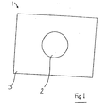
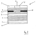
- One type of laser diode is the vertical cavity surface emission laser diode (VCSEL), and a typical example is shown in plan view in Figure 1 and in side cross-sectional view in Figure 2 of the accompanying drawings.
- the VCSEL 1 comprises a substrate 7, which carries a lower electrical contact 8.
- An active region 6 is sandwiched between upper and lower distributed Bragg reflector (DBR) mirror structures 4 and 5, the lower mirror structure being carried by the substrate 7.
- the mirror structures 4 and 5 provide high reflectivity, for example around 99.5%.
- the upper DBR mirror structure 4 includes a proton implant area 9.
- the proton implant area 9 serves to confine current supplied to the device.
- An upper electrical contact 3 is provided on the upper surface of the upper mirror structure 4.
- the upper contact 3 defines an aperture 2 through to the upper surface of the upper mirror structure 4.
- the VCSEL 1 of Figures 1 and 2 produces a light output which is emitted in the direction of arrow A through the aperture 2.
- the output light is produced by a lasing effect or laser action in the active region 6 between the two DBR mirrors 4 and 5, as is well known.
- VCSEL devices One of the main advantages of VCSEL devices is that the light output is produced in a direction perpendicular to the plane of the device. This is in contrast to previous edge emitting laser diodes which emit light in the plane of the device.
- VCSEL devices can easily be manufactured into arrays, since a number of devices can be produced on a single semiconductor area, without the need for the devices to be cut from one another.
- VCSELs are particularly suited for producing a circular beam of light. Such a circular beam requires little or no further optical processing before application to devices, such as CD ROM drives or communications devices.
- laser emission in VCSELs can often allow orthogonal or elliptical polarisation states, with incomplete control of the orientation of the axes of polarisation or the polarisation state of individual lasing modes or filaments, which may also vary with the bias current. This can also result in the orientation of the polarisation axes varying from device to device even between adjacent lasers fabricated from the same wafer.
- VCSELs vertical-cavity surface-emitting lasers
- these applications tend to require high beam quality, in particular with single transverse mode operation where the polarisation state is fixed to a precise direction.
- VCSELs can be formed to generate circular beams and integrated in two dimensional arrays, they suffer from strong optical nonlinearities associated with their high gain operation and strong thermal effects. Such nonlinearities can cause not just strong multimode operation but also filamentary action across the emitting region. This behaviour thus causes beams to be generated with poor far fields and with multiple intensity peaks emitting in poorly defined polarisation states, which can vary with temperature and bias current.
- Integration of additional structures with the laser can provide polarisation control but significantly increase the complexity of the device, and such structures can influence the spatial output characteristics of the laser emission.
- a vertical cavity surface emitting laser device having a void formed within the body of the device, such that, when the device is in use, the direction of polarisation of light emitted from the device is substantially aligned with a boundary of the discontinuity.
- the void may be provided by an elongated trench which extends into the body of the device from an outer surface thereof.
- Such a device may comprise a plurality of such voids, the polarisation direction of light emitted by the device when in use being determined by the voids.
- a pair of substantially parallel elongate voids may be provided, the direction of polarisation of the emitted light being substantially aligned with the direction of the boundary of the voids which is closest to the light output region.
- a pair of substantially mutually orthogonal elongate voids may be used.
- At least one of the mirror structures may be a distributed Bragg reflector structure.
- the trench region may be formed by etching the device structure, or by laser ablation of the device structure, or by electron beam lithography.
- the semiconductor material of the device preferably allows light emission in the 400nm - 4000 nm wavelength range.
- a method of polarising light comprising forming a void in the body of a vertical cavity surface emitting laser device, such that the polarisation direction of light emitted from the device when in use is substantially aligned with a boundary of the void.
- FIGS. 3 and 4 of the accompanying drawings show plan and cross-sectional views respectively of a VCSEL diode 10 embodying the present invention.
- the VCSEL 10 comprises a pair of electrodes 13 and 18, a substrate material 17, and an active area 16 which is sandwiched between upper and lower DBR mirror structures 14 and 15.
- the upper DBR mirror structure incorporates a proton implant area 19.
- the upper electrode 13 defines a circular aperture 12 through which laser light is emitted in the direction of arrow A.
- the VCSEL shown in Figures 3 and 4 operates substantially in accordance with the known device of Figures 1 and 2, in as much as a lasing effect is produced in the active area 16 between the two mirror structures 14 and 15. Light produced by this effect is then emitted through the aperture 12, as before.
- polarisation control of the emitted laser light is achieved by the introduction of a void into the device.
- the void is provided by an etched trench 11 which extends through the upper electrode 13 into the DBR mirror structure 14, toward the active region 16.
- the etched trench adjacent to the lasing aperture is preferably positioned at a distance of up to 10 microns from the edge of the aperture ( Figure 4).
- the trench discontinuity can be introduced by masking and etching techniques, or other techniques such as micromachining, laser ablation, e-beam lithography, X-ray or reactive ion etching (RIE), and may be carried out on completed devices.
- masking and etching techniques or other techniques such as micromachining, laser ablation, e-beam lithography, X-ray or reactive ion etching (RIE), and may be carried out on completed devices.
- the void can be provided by means other than a trench.
- the voids described in this description are merely exemplary, and the skilled person will be able to design further voids within the scope of the invention.
- the orientation of the void may be varied to tune the polarisation state of emission to a preferred/desired orientation.
- the angle of the void profile from the normal to the plane of the device emission plane can vary, as can its depth, allowing penetration through other layers such as the active region 16 and the lower mirror structure 15.
- the width, length and shape of the refractive index void 11 can also vary.
- the use of a trench or other void allows the axis of the dominant polarisation to be set at any desired orientation, independent of any pre-existing effect, such as orientation of the crystal axes.
- the polarisation of the output light beam aligns with the direction of the closest boundary of the discontinuity to the aperture.
- a deep trench has more effect on the polarisation pinning than a shallow trench.
- a trench which is close in to the aperture 12 will have more effect than a trench which is spaced apart from the aperture.
- This method of achieving polarisation control is applicable to optically pumped and electrically pumped laser devices.
- the semiconductor material used for devices according to the invention preferably allows emission in the 400nm - 4000nm wavelength range.
- the polarisation control of the invention need not significantly degrade the quality of the spatial, spectral and power output characteristics of the laser, nor the electrical characteristics of the laser, as will be illustrated below.
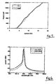
- Figure 5, 6 and 7 show that the key performance areas of the device are not seriously degraded by the method for polarisation control, with no degradation of the light power output/current characteristics, the optical spectrum or the spatial output.
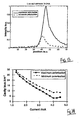
- Figure 8 shows the L-I characteristics for a typical proton implanted VCSEL, in which poor single polarisation operation occurs.
- switching of the polarisation state is observed, and at high currents both polarisations occur together.
- Figures 9 and 10 show the influence of polarisation control on the above-threshold polarisation dependent power measurements, showing how emission from one polarisation state remains highly suppressed over the entire device operating range in a device embodying the invention. Following the etching of a trench, 1 micron wide, 7 microns from the edge of the aperture and between 4 and 4.5 microns deep, single polarisation operation is forced (Figure 9).
- Figures 11 and 12 show the influence of etching on the sub-threshold polarisation-dependent power from the cavity aperture of respective modified VCSEL devices, showing that modification results in unequal splitting between the two polarisation states, even at bias currents well below threshold.
- Figure 13 shows that power measurements of the spontaneous emission from the etched line display a high polarisation dependency.
- Figure 14 shows the introduction of polarisation dependent cavity loss, related to the sub-threshold line width of emission and Figure 15 shows spectral splitting of the orthogonal polarisation states, introduced through modification of the laser.
- Successful pinning of polarisation requires trenches to be formed of sufficient depth, and these must at least pass through the top metallic contact layers into the semiconductor material.
- the minimum depth required for pinning depends on the distance of the trench from the aperture and also the direction of the trench with respect to that of the existing polarisation direction, as the pinning mechanism has to overcome existing polarisation selection mechanisms before setting the polarisation to it own direction.
- the depth must also be sufficiently great in multimode devices to ensure that all modes are polarised, care being required in this respect as higher order modes frequently are generated with orthogonal polarisations.
- a laser diode embodying the present invention may incorporate more than one void, for example as shown in Figures 16 and 17.
- two parallel voids are shown, one to each side of the aperture 22 of the device.
- Figure 17 shows a device having a pair of orthogonal etches.
- the polarisation direction will align with the direction of the two voids.
- the Figure 17 example can be used to set the cavity gain of two orthogonal polarisations to be equal.
Landscapes
- Physics & Mathematics (AREA)
- Electromagnetism (AREA)
- Optics & Photonics (AREA)
- Condensed Matter Physics & Semiconductors (AREA)
- General Physics & Mathematics (AREA)
- Engineering & Computer Science (AREA)
- Plasma & Fusion (AREA)
- Semiconductor Lasers (AREA)
- Pinball Game Machines (AREA)
- Lasers (AREA)
- Laser Surgery Devices (AREA)
Abstract
Description
- The present invention relates to laser devices, and in particular to vertical cavity surface emitting laser (VCSEL) devices such as VCSEL diodes.
- Laser devices, such as laser diodes, are being increasingly used in a variety of applications, such as communications and data storage devices. One type of laser diode is the vertical cavity surface emission laser diode (VCSEL), and a typical example is shown in plan view in Figure 1 and in side cross-sectional view in Figure 2 of the accompanying drawings. The VCSEL 1 comprises a
substrate 7, which carries a lowerelectrical contact 8. Anactive region 6 is sandwiched between upper and lower distributed Bragg reflector (DBR)mirror structures substrate 7. Themirror structures DBR mirror structure 4 includes aproton implant area 9. Theproton implant area 9 serves to confine current supplied to the device. - An upper
electrical contact 3 is provided on the upper surface of theupper mirror structure 4. Theupper contact 3 defines anaperture 2 through to the upper surface of theupper mirror structure 4. - The
VCSEL 1 of Figures 1 and 2 produces a light output which is emitted in the direction of arrow A through theaperture 2. The output light is produced by a lasing effect or laser action in theactive region 6 between the twoDBR mirrors - One of the main advantages of VCSEL devices is that the light output is produced in a direction perpendicular to the plane of the device. This is in contrast to previous edge emitting laser diodes which emit light in the plane of the device. Thus, VCSEL devices can easily be manufactured into arrays, since a number of devices can be produced on a single semiconductor area, without the need for the devices to be cut from one another. In addition, VCSELs are particularly suited for producing a circular beam of light. Such a circular beam requires little or no further optical processing before application to devices, such as CD ROM drives or communications devices.
- However, laser emission in VCSELs can often allow orthogonal or elliptical polarisation states, with incomplete control of the orientation of the axes of polarisation or the polarisation state of individual lasing modes or filaments, which may also vary with the bias current. This can also result in the orientation of the polarisation axes varying from device to device even between adjacent lasers fabricated from the same wafer.
- There is much interest in the use of vertical-cavity surface-emitting lasers (VCSELs) for a variety of applications including optical storage, printing and communications. However these applications tend to require high beam quality, in particular with single transverse mode operation where the polarisation state is fixed to a precise direction. Although VCSELs can be formed to generate circular beams and integrated in two dimensional arrays, they suffer from strong optical nonlinearities associated with their high gain operation and strong thermal effects. Such nonlinearities can cause not just strong multimode operation but also filamentary action across the emitting region. This behaviour thus causes beams to be generated with poor far fields and with multiple intensity peaks emitting in poorly defined polarisation states, which can vary with temperature and bias current.
- Previous methods for controlling the polarisation state of light emitted from surface-emitting lasers have included the use of anisotropic cavity geometries which may cause distortion of the output beam shape. Introduction of anisotropic stress, gain or loss has also been used for control of polarisation state along pre-defined directions, though complete control is not usually maintained over the entire device operating range.
- Temperature detuning of non-degenerate cavity modes has been used for complete polarisation control but this is achieved at the expense of reducing the gain, thereby increasing the device threshold current and power consumption and reducing the available power output. This effect is strongly dependent on the spectral splitting of orthogonal polarisation states, which may be influenced by the residual strain in a device. Therefore an additional technique may be required to control the spectral splitting if a sufficient gain difference is to be achieved between the two states.
- Integration of additional structures with the laser, for example gratings, can provide polarisation control but significantly increase the complexity of the device, and such structures can influence the spatial output characteristics of the laser emission.
- IEEE Photon. Technol. Lett., vol. 5, no.2, February 1993, pages 133-135, discloses a vertical cavity surface emitting laser emitting a polarized beam caused by anisotropic stress due to an elliptical substrate hole.
- According to one aspect of the present invention as defined in
claim 1 there is provided a vertical cavity surface emitting laser device having a void formed within the body of the device, such that, when the device is in use, the direction of polarisation of light emitted from the device is substantially aligned with a boundary of the discontinuity. - The void may be provided by an elongated trench which extends into the body of the device from an outer surface thereof.
- Such a device may comprise a plurality of such voids, the polarisation direction of light emitted by the device when in use being determined by the voids.
- A pair of substantially parallel elongate voids may be provided, the direction of polarisation of the emitted light being substantially aligned with the direction of the boundary of the voids which is closest to the light output region.
- Alternatively, a pair of substantially mutually orthogonal elongate voids may be used.
- In such a device at least one of the mirror structures may be a distributed Bragg reflector structure.
- The trench region may be formed by etching the device structure, or by laser ablation of the device structure, or by electron beam lithography.
- The semiconductor material of the device preferably allows light emission in the 400nm - 4000 nm wavelength range.
- According to another aspect of the present invention as defined in
claim 11, there is provided a method of polarising light comprising forming a void in the body of a vertical cavity surface emitting laser device, such that the polarisation direction of light emitted from the device when in use is substantially aligned with a boundary of the void. - Figures 1 and 2 show plan and cross-sectional views respectively of a known VCSEL diode;
- Figures 3 and 4 show plan and cross-sectional views of a preferred embodiment of the present invention;
- Figure 5 is a graph comparing light current L-I characteristics of a known VCSEL and a VCSEL embodying the present invention;
- Figure 6 is a graph of L-I characteristics of a known laser diode;
- Figure 7 shows the L-I characteristics of an embodiment of the present invention;
- Figures 8, 9 and 10 are graphs illustrating the above-threshold polarisation dependent power measurements of an embodiment of the present invention;
- Figure 11 is a graph comparing sub-threshold polarisation dependent L-I characteristics of a known laser diode with a diode embodying the present invention;
- Figure 12 is a graph of sub-threshold polarisation ratio measurements of a known laser diode and a laser diode embodying the invention;
- Figure 13 is a graph illustrating cross-section through line emission showing the polarisation dependency of output power of an embodiment of the present invention;
- Figure 14 is a graph indicating polarisation resolved cavity loss measurements of a laser diode embodying the present invention;
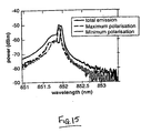
- Figure 15 is a graph illustrating sub-threshold optical spectra of a laser diode device embodying the present invention;
- Figure 16 shows a plan view of a second laser diode embodying the present invention; and
- Figure 17 shows a plan view of a third laser diode embodying the present invention.
- Figures 3 and 4 of the accompanying drawings show plan and cross-sectional views respectively of a
VCSEL diode 10 embodying the present invention. - As described with reference to a known device above, the
VCSEL 10 comprises a pair ofelectrodes substrate material 17, and anactive area 16 which is sandwiched between upper and lowerDBR mirror structures proton implant area 19. Theupper electrode 13 defines acircular aperture 12 through which laser light is emitted in the direction of arrow A. - The VCSEL shown in Figures 3 and 4 operates substantially in accordance with the known device of Figures 1 and 2, in as much as a lasing effect is produced in the
active area 16 between the twomirror structures aperture 12, as before. - However, in the present invention, polarisation control of the emitted laser light is achieved by the introduction of a void into the device. In the device shown in Figure 4, the void is provided by an etched
trench 11 which extends through theupper electrode 13 into theDBR mirror structure 14, toward theactive region 16. - The etched trench adjacent to the lasing aperture is preferably positioned at a distance of up to 10 microns from the edge of the aperture (Figure 4).
- The trench discontinuity can be introduced by masking and etching techniques, or other techniques such as micromachining, laser ablation, e-beam lithography, X-ray or reactive ion etching (RIE), and may be carried out on completed devices.
- Other geometries and positions for such etches may also produce desirable results.
- The void can be provided by means other than a trench. The voids described in this description are merely exemplary, and the skilled person will be able to design further voids within the scope of the invention.
- The orientation of the void may be varied to tune the polarisation state of emission to a preferred/desired orientation. The angle of the void profile from the normal to the plane of the device emission plane can vary, as can its depth, allowing penetration through other layers such as the
active region 16 and thelower mirror structure 15. The width, length and shape of therefractive index void 11 can also vary. - The introduction of a trench modifies the stress and strain experienced by the device, which controls the polarisation dependence of the emitted light beam. There also appear to be boundary effects that control the polarisation.
- The introduction of trenches seems also to introduce a further effect which causes a polarisation dependence of the optical mode density and results in the spontaneous emission displaying a similar polarisation dependence to the lasing emission.
- The use of a trench or other void allows the axis of the dominant polarisation to be set at any desired orientation, independent of any pre-existing effect, such as orientation of the crystal axes. The polarisation of the output light beam aligns with the direction of the closest boundary of the discontinuity to the aperture.
- In general terms, a deep trench has more effect on the polarisation pinning than a shallow trench. A trench which is close in to the
aperture 12 will have more effect than a trench which is spaced apart from the aperture. - This method of achieving polarisation control is applicable to optically pumped and electrically pumped laser devices.
- The semiconductor material used for devices according to the invention preferably allows emission in the 400nm - 4000nm wavelength range.
- The polarisation control of the invention need not significantly degrade the quality of the spatial, spectral and power output characteristics of the laser, nor the electrical characteristics of the laser, as will be illustrated below.
- Figure 5, 6 and 7 show that the key performance areas of the device are not seriously degraded by the method for polarisation control, with no degradation of the light power output/current characteristics, the optical spectrum or the spatial output.
- Figure 8 shows the L-I characteristics for a typical proton implanted VCSEL, in which poor single polarisation operation occurs. Here, on the onset of higher order transverse modes, switching of the polarisation state is observed, and at high currents both polarisations occur together.
- Figures 9 and 10 show the influence of polarisation control on the above-threshold polarisation dependent power measurements, showing how emission from one polarisation state remains highly suppressed over the entire device operating range in a device embodying the invention. Following the etching of a trench, 1 micron wide, 7 microns from the edge of the aperture and between 4 and 4.5 microns deep, single polarisation operation is forced (Figure 9).
- This is achieved with minimal change in threshold current or device efficiency. The polarisation state of emission remains fixed throughout the device bias current operating range, with the dominant E field polarisation parallel to the etch direction. Polarisation extinction ratios in excess of 100 (Figure 10) are achieved and only found to reduce significantly on the onset of thermal roll off. Indeed the etching of the trench is found to polarise the spontaneous emission significantly, causing extinction ratios as high as 1.5 at low drive currents in the centre of the etch, rising to 3 at the etch. The pinning mechanisms are very strong, unlike in other devices, causing immediate single polarisation operation immediately from turn-on when a device is pulsed rather than the initial polarisation competition before a steady state equilibrium is reached in non-controlled devices. Despite the proximity of the etch to the aperture, no adverse effects are seen in terms of lifetime.
- This technique has been applied to a wide range of devices and is found to be always successful. The polarisation direction in all cases aligns itself along the etch direction and remains fixed in this direction at least to within 5 degrees, this being the limit of accuracy of the measurement.
- Figures 11 and 12 show the influence of etching on the sub-threshold polarisation-dependent power from the cavity aperture of respective modified VCSEL devices, showing that modification results in unequal splitting between the two polarisation states, even at bias currents well below threshold.
- Figure 13 shows that power measurements of the spontaneous emission from the etched line display a high polarisation dependency.
- Figure 14 shows the introduction of polarisation dependent cavity loss, related to the sub-threshold line width of emission and Figure 15 shows spectral splitting of the orthogonal polarisation states, introduced through modification of the laser.
- As the etches applied adjacent to the emitting aperture do not strongly affect the lasing mode, high spectral quality circuit output beam characteristics can be obtained for the single-mode operating regime of multimode devices as well as for monomode devices. In addition, longitudinal monomode operation, if achieved before polarisation pinning, is retained (Figure 15). A small shift in line width is observed though this is small (< 0.2 nm), the dominant polarisation being observed at the shorter wavelength. This shows that the polarisation pinning mechanism can cause enhanced birefringence in the system.
- Successful pinning of polarisation requires trenches to be formed of sufficient depth, and these must at least pass through the top metallic contact layers into the semiconductor material. The minimum depth required for pinning depends on the distance of the trench from the aperture and also the direction of the trench with respect to that of the existing polarisation direction, as the pinning mechanism has to overcome existing polarisation selection mechanisms before setting the polarisation to it own direction. The depth must also be sufficiently great in multimode devices to ensure that all modes are polarised, care being required in this respect as higher order modes frequently are generated with orthogonal polarisations.
- An assessment of the cavity losses associated with each polarisation state has been carried out by measuring the polarisation-resolved line widths below threshold. It can be seen from Figure 14 that the measured cavity losses experienced by the dominant polarisation state are smaller than those for the highly suppressed state. Prior to etching, the spectral splitting was not observed and the cavity losses of the two polarisation states were found to be similar. Indeed optical injection measurements, where the photogenerated current from a VCSEL when used as a detector is measured have shown there to be a polarisation dependent absorption after etching, this indicating a modification in the band-edge driven probably by a strain dependent effect.
- A laser diode embodying the present invention may incorporate more than one void, for example as shown in Figures 16 and 17. In Figure 16, two parallel voids are shown, one to each side of the
aperture 22 of the device. Figure 17 shows a device having a pair of orthogonal etches. - In the example shown in figure 16, the polarisation direction will align with the direction of the two voids. The Figure 17 example can be used to set the cavity gain of two orthogonal polarisations to be equal.
Claims (11)
- A vertical cavity surface emitting laser device (10) having a discontinuity (11) formed within the body (13, 14, 15, 18, 17, 18) of the device, such that, when the device is in use, the direction of polarisation of light emitted from the device is substantially aligned with a boundary of the discontinuity (11), characterised in that the discontinuity (11) is formed by a void.
- A device as claimed in claim 1, comprising a substrate (17), a lower mirror structure (15) carried by the substrate, an active region (16) carried by the lower mirror structure, and an upper mirror structure (14) carried by the active region, and a contact region (13) carried by the upper mirror structure, the contact region defining an aperture (12) through which laser light is emitted when the diode is in use.
- A device as claimed in claim 2, wherein at least one of the mirror structures is a distributed Bragg reflector structure.
- A device as claimed in claim 1, wherein the void is provided by an elongate trench (11) which extends into the body of the device from an outer surface thereof.
- A device as claimed in any one of claims 1 to 4, comprising a plurality of such discontinuities (211, 212, 311, 322), the polarisation direction of light emitted by the device when in use being determined by the discontinuities.
- A device as claimed in claim 5, comprising a pair of substantially parallel elongate discontinuities (211, 212), the direction of polarisation of the emitted light being substantially aligned with the elongate direction of the discontinuities.
- A device as claimed in claim 5, comprising a pair of substantially orthogonal elongate discontinuities (311, 312).
- A device as claimed in claim 2, wherein the void is provided by a trench region (11) which extends through the contact region (13) into the device towards the active region (16).
- A device as claimed In any one of the preceding claims, including semiconductor materials which allows light emission in the 400nm - 4000nm wavelength range.
- A method of polarising light comprising forming a discontinuity in the body of a vertical cavity surface emitting laser device, such that the polarisation direction of light emitted from the device when in use Is substantially aligned with a boundary of the discontinuity, characterised in that the discontinuity is formed by forming a void in the body of the device.
- A method as claimed in claim 10, comprising forming a trench region in the body of the device, which trench region extends from an outer surface of the device.
Priority Applications (1)
| Application Number | Priority Date | Filing Date | Title |
|---|---|---|---|
| EP05026522A EP1679773A3 (en) | 1997-05-17 | 1998-05-15 | Laser devices |
Applications Claiming Priority (3)
| Application Number | Priority Date | Filing Date | Title |
|---|---|---|---|
| GBGB9709949.3A GB9709949D0 (en) | 1997-05-17 | 1997-05-17 | Vertical-cavity surface-emitting laser polarisation control |
| GB9709949 | 1997-05-17 | ||
| PCT/GB1998/001415 WO1998053537A1 (en) | 1997-05-17 | 1998-05-15 | Laser devices |
Related Child Applications (1)
| Application Number | Title | Priority Date | Filing Date |
|---|---|---|---|
| EP05026522A Division EP1679773A3 (en) | 1997-05-17 | 1998-05-15 | Laser devices |
Publications (2)
| Publication Number | Publication Date |
|---|---|
| EP0981843A1 EP0981843A1 (en) | 2000-03-01 |
| EP0981843B1 true EP0981843B1 (en) | 2006-03-08 |
Family
ID=10812411
Family Applications (2)
| Application Number | Title | Priority Date | Filing Date |
|---|---|---|---|
| EP98921631A Expired - Lifetime EP0981843B1 (en) | 1997-05-17 | 1998-05-15 | Laser devices |
| EP05026522A Withdrawn EP1679773A3 (en) | 1997-05-17 | 1998-05-15 | Laser devices |
Family Applications After (1)
| Application Number | Title | Priority Date | Filing Date |
|---|---|---|---|
| EP05026522A Withdrawn EP1679773A3 (en) | 1997-05-17 | 1998-05-15 | Laser devices |
Country Status (9)
| Country | Link |
|---|---|
| US (1) | US6639931B1 (en) |
| EP (2) | EP0981843B1 (en) |
| JP (1) | JP3955925B2 (en) |
| KR (1) | KR100566027B1 (en) |
| CN (1) | CN1120550C (en) |
| AT (1) | ATE320098T1 (en) |
| DE (1) | DE69833754T2 (en) |
| GB (1) | GB9709949D0 (en) |
| WO (1) | WO1998053537A1 (en) |
Families Citing this family (30)
| Publication number | Priority date | Publication date | Assignee | Title |
|---|---|---|---|---|
| US6304588B1 (en) * | 1997-02-07 | 2001-10-16 | Xerox Corporation | Method and structure for eliminating polarization instability in laterally-oxidized VCSELs |
| JP3482824B2 (en) | 1997-07-29 | 2004-01-06 | セイコーエプソン株式会社 | Surface emitting semiconductor laser and surface emitting semiconductor laser array |
| US6188711B1 (en) * | 1997-12-18 | 2001-02-13 | Agilent Technologies, Inc. | Polarization-controlled VCSELs using externally applied uniaxial stress |
| US6961521B1 (en) * | 2001-03-27 | 2005-11-01 | Turin Networks | Method and apparatus for transmitting a bit interleaved optical data stream on an optical network |
| US20060003477A1 (en) * | 2002-10-30 | 2006-01-05 | Bert Braune | Method for producing a light source provided with electroluminescent diodes and comprising a luminescence conversion element |
| TW565975B (en) * | 2002-12-27 | 2003-12-11 | Ind Tech Res Inst | Oxide confined type vertical cavity surface emitting laser device and the manufacturing method thereof |
| JP2005086170A (en) * | 2003-09-11 | 2005-03-31 | Seiko Epson Corp | Surface emitting semiconductor laser and manufacturing method thereof |
| US7218660B2 (en) * | 2003-10-27 | 2007-05-15 | Avago Technologies Fiber Ip (Singapore) Pte. Ltd. | Single-mode vertical cavity surface emitting lasers and methods of making the same |
| DE102004005269B4 (en) * | 2003-11-28 | 2005-09-29 | Osram Opto Semiconductors Gmbh | Light emitting semiconductor element has multilayers on a substrate with the pn junction insulatively separated into light emitting and protective diode sections |
| US7419912B2 (en) * | 2004-04-01 | 2008-09-02 | Cree, Inc. | Laser patterning of light emitting devices |
| US7372886B2 (en) * | 2004-06-07 | 2008-05-13 | Avago Technologies Fiber Ip Pte Ltd | High thermal conductivity vertical cavity surface emitting laser (VCSEL) |
| JP4687064B2 (en) * | 2004-10-22 | 2011-05-25 | ソニー株式会社 | Surface emitting semiconductor laser device |
| JP5376104B2 (en) * | 2005-07-04 | 2013-12-25 | ソニー株式会社 | Surface emitting semiconductor laser |
| US7400661B2 (en) * | 2006-11-08 | 2008-07-15 | Lexmark International, Inc. | Automatic setting of laser diode bias current |
| JP4992503B2 (en) | 2007-03-27 | 2012-08-08 | ソニー株式会社 | Surface emitting semiconductor laser and manufacturing method thereof |
| JP5445806B2 (en) * | 2008-11-27 | 2014-03-19 | 株式会社リコー | Surface emitting laser element, surface emitting laser array, optical scanning device, and image forming apparatus |
| JP5261754B2 (en) | 2008-11-27 | 2013-08-14 | 株式会社リコー | Surface emitting laser element, surface emitting laser array, optical scanning device, and image forming apparatus |
| JP5326677B2 (en) | 2009-03-09 | 2013-10-30 | ソニー株式会社 | Semiconductor laser and manufacturing method thereof |
| JP5510899B2 (en) | 2009-09-18 | 2014-06-04 | 株式会社リコー | Surface emitting laser element, surface emitting laser array, optical scanning device, and image forming apparatus |
| JP5532321B2 (en) | 2009-11-17 | 2014-06-25 | 株式会社リコー | Surface emitting laser element, surface emitting laser array, optical scanning device, and image forming apparatus |
| JP2011151357A (en) | 2009-12-21 | 2011-08-04 | Ricoh Co Ltd | Optical device, optical scanning apparatus, and image forming apparatus |
| JP2011159943A (en) * | 2010-01-08 | 2011-08-18 | Ricoh Co Ltd | Surface emitting laser element, surface emitting laser array, optical scanner device, and image forming apparatus |
| JP5601014B2 (en) | 2010-04-23 | 2014-10-08 | 株式会社リコー | Optical device, optical scanning apparatus, and image forming apparatus |
| DE102011100175B4 (en) * | 2011-05-02 | 2021-12-23 | OSRAM Opto Semiconductors Gesellschaft mit beschränkter Haftung | Laser light source with a ridge waveguide structure and a mode filter structure |
| JP5874227B2 (en) * | 2011-07-22 | 2016-03-02 | 富士ゼロックス株式会社 | Surface emitting semiconductor laser array, surface emitting semiconductor laser device, optical transmission device, and information processing device |
| JP2014017448A (en) * | 2012-07-11 | 2014-01-30 | Ricoh Co Ltd | Surface emitting laser, surface emitting laser array, optical scanner device and image forming device |
| EP3093194B1 (en) | 2015-04-24 | 2021-09-22 | Ricoh Company, Ltd. | Information provision device |
| JP2016213412A (en) | 2015-05-13 | 2016-12-15 | 株式会社リコー | Optical device and light irradiation device |
| JP6786961B2 (en) * | 2016-08-29 | 2020-11-18 | セイコーエプソン株式会社 | Surface emitting laser and atomic oscillator |
| CN111435781B (en) * | 2019-01-15 | 2022-03-18 | 中国科学院半导体研究所 | Vertical Cavity Surface Emitting Semiconductor Laser Structure |
Family Cites Families (13)
| Publication number | Priority date | Publication date | Assignee | Title |
|---|---|---|---|---|
| US5295148A (en) * | 1990-09-12 | 1994-03-15 | Seiko Epson Corporation | Surface emission type semiconductor laser |
| JP2961964B2 (en) * | 1991-07-10 | 1999-10-12 | 日本電気株式会社 | Semiconductor laser device |
| US5293392A (en) * | 1992-07-31 | 1994-03-08 | Motorola, Inc. | Top emitting VCSEL with etch stop layer |
| JPH0770790B2 (en) * | 1992-11-27 | 1995-07-31 | 日本電気株式会社 | Surface emitting element |
| US5331654A (en) * | 1993-03-05 | 1994-07-19 | Photonics Research Incorporated | Polarized surface-emitting laser |
| US5412680A (en) * | 1994-03-18 | 1995-05-02 | Photonics Research Incorporated | Linear polarization of semiconductor laser |
| US5729563A (en) * | 1994-07-07 | 1998-03-17 | Hewlett-Packard Company | Method and apparatus for optically and thermally isolating surface emitting laser diodes |
| US5493577A (en) * | 1994-12-21 | 1996-02-20 | Sandia Corporation | Efficient semiconductor light-emitting device and method |
| US5568499A (en) * | 1995-04-07 | 1996-10-22 | Sandia Corporation | Optical device with low electrical and thermal resistance bragg reflectors |
| US5727014A (en) * | 1995-10-31 | 1998-03-10 | Hewlett-Packard Company | Vertical-cavity surface-emitting laser generating light with a defined direction of polarization |
| US5757836A (en) * | 1996-07-01 | 1998-05-26 | Motorola, Inc. | Vertical cavity surface emitting laser with laterally integrated photodetector |
| US5953362A (en) * | 1997-12-15 | 1999-09-14 | Pamulapati; Jagadeesh | Strain induce control of polarization states in vertical cavity surface emitting lasers and method of making same |
| US6185240B1 (en) * | 1998-01-30 | 2001-02-06 | Motorola, Inc. | Semiconductor laser having electro-static discharge protection |
-
1997
- 1997-05-17 GB GBGB9709949.3A patent/GB9709949D0/en active Pending
-
1998
- 1998-05-15 EP EP98921631A patent/EP0981843B1/en not_active Expired - Lifetime
- 1998-05-15 EP EP05026522A patent/EP1679773A3/en not_active Withdrawn
- 1998-05-15 AT AT98921631T patent/ATE320098T1/en not_active IP Right Cessation
- 1998-05-15 CN CN98807183A patent/CN1120550C/en not_active Expired - Lifetime
- 1998-05-15 WO PCT/GB1998/001415 patent/WO1998053537A1/en not_active Ceased
- 1998-05-15 US US09/424,011 patent/US6639931B1/en not_active Expired - Lifetime
- 1998-05-15 JP JP55010198A patent/JP3955925B2/en not_active Expired - Lifetime
- 1998-05-15 KR KR1019997010641A patent/KR100566027B1/en not_active Expired - Lifetime
- 1998-05-15 DE DE69833754T patent/DE69833754T2/en not_active Expired - Lifetime
Non-Patent Citations (2)
| Title |
|---|
| CHAVEZ-PIRSON A. ET AL: "POLARIZATION PROPERTIES OF A VERTICAL CAVITY SURFACE EMITTING LASER USING A FRACTIONAL LAYER SUPERLATTICE GAIN MEDIUM", APPLIED PHYSICS LETTERS, vol. 62, no. 24, 14 June 1993 (1993-06-14), NEW YORK, pages 3082 - 3084 * |
| MUKAIHARA T. ET AL: "ENGINEERED POLARIZATION CONTROL OF GAAS/ALGAAS SURFACE-EMITTING LASERS BY ANISOTROPIC STRESS FROM ELLIPTICAL ETCHED SUBSTRATE HOLE", IEEE PHOTONICS TECHNOLOGY LETTERS, vol. 5, no. 2, February 1993 (1993-02-01), pages 133 - 135 * |
Also Published As
| Publication number | Publication date |
|---|---|
| GB9709949D0 (en) | 1997-07-09 |
| EP1679773A3 (en) | 2009-02-11 |
| JP2001525995A (en) | 2001-12-11 |
| EP0981843A1 (en) | 2000-03-01 |
| DE69833754D1 (en) | 2006-05-04 |
| US6639931B1 (en) | 2003-10-28 |
| WO1998053537A1 (en) | 1998-11-26 |
| KR20010012680A (en) | 2001-02-26 |
| JP3955925B2 (en) | 2007-08-08 |
| ATE320098T1 (en) | 2006-03-15 |
| CN1263642A (en) | 2000-08-16 |
| DE69833754T2 (en) | 2006-11-30 |
| EP1679773A2 (en) | 2006-07-12 |
| KR100566027B1 (en) | 2006-03-30 |
| CN1120550C (en) | 2003-09-03 |
Similar Documents
| Publication | Publication Date | Title |
|---|---|---|
| US6639931B1 (en) | Laser devices | |
| US4873696A (en) | Surface-emitting lasers with periodic gain and a parallel driven nipi structure | |
| US6885690B2 (en) | Transverse mode and polarization control of surface emitting lasers through the formation of a dielectric stack | |
| EP3453086B1 (en) | Laser device and method for its operation | |
| US7333522B2 (en) | Polarization control of vertical diode lasers by monolithically integrated surface grating | |
| EP3869642B1 (en) | Vertical resonator-type light-emitting element | |
| US5272711A (en) | High-power semiconductor laser diode | |
| Vail et al. | High performance micromechanical tunable vertical cavity surface emitting lasers | |
| US6188711B1 (en) | Polarization-controlled VCSELs using externally applied uniaxial stress | |
| Verschaffelt et al. | Polarisation switching in vertical-cavity surface-emitting lasers: from experimental observations to applications | |
| EP1104056A1 (en) | A polarization controlled vertical-cavity surface-emitting laser | |
| US5539759A (en) | Single mode laser with a passive antiguide region | |
| Unold et al. | Polarisation control in VCSELs by elliptic surface etching | |
| KR100404043B1 (en) | Vertically integrated high-power surface-emitting laser diode and method of manufacturing the same | |
| US6567454B1 (en) | Coupled-resonator vertical-cavity lasers with two active gain regions | |
| WO2006136346A1 (en) | Monolithic micro-lasers with stabilised polarisation | |
| Ha et al. | Polarisation anisotropy in asymmetric oxide aperture VCSELs | |
| KR100553953B1 (en) | Optical polarization method of laser device | |
| Li et al. | Multi-/spl lambda/ridge waveguide gain-coupled DFB laser array | |
| KR100553955B1 (en) | Laser device | |
| Choquette et al. | Polarization characteristics, control, and modulation of vertical-cavity surface emitting lasers | |
| Riedl et al. | Approaches for Polarization Control in VCSELs | |
| Nakamura et al. | Single-mode oxide-confined VCSEL for printers and sensors | |
| KR20050090468A (en) | Method for producing a waveguide structure in a surface-emitting semiconductor laser and surface-emitting semiconductor laser | |
| HK40059814A (en) | Laser device and method for its operation |
Legal Events
| Date | Code | Title | Description |
|---|---|---|---|
| PUAI | Public reference made under article 153(3) epc to a published international application that has entered the european phase |
Free format text: ORIGINAL CODE: 0009012 |
|
| 17P | Request for examination filed |
Effective date: 19991208 |
|
| AK | Designated contracting states |
Kind code of ref document: A1 Designated state(s): AT BE CH CY DE DK ES FI FR GB GR IE IT LI LU MC NL PT SE |
|
| 17Q | First examination report despatched |
Effective date: 20001214 |
|
| GRAP | Despatch of communication of intention to grant a patent |
Free format text: ORIGINAL CODE: EPIDOSNIGR1 |
|
| RIC1 | Information provided on ipc code assigned before grant |
Ipc: 7H 01S 5/183 A |
|
| GRAS | Grant fee paid |
Free format text: ORIGINAL CODE: EPIDOSNIGR3 |
|
| GRAA | (expected) grant |
Free format text: ORIGINAL CODE: 0009210 |
|
| AK | Designated contracting states |
Kind code of ref document: B1 Designated state(s): AT BE CH CY DE DK ES FI FR GB GR IE IT LI LU MC NL PT SE |
|
| PG25 | Lapsed in a contracting state [announced via postgrant information from national office to epo] |
Ref country code: NL Free format text: LAPSE BECAUSE OF FAILURE TO SUBMIT A TRANSLATION OF THE DESCRIPTION OR TO PAY THE FEE WITHIN THE PRESCRIBED TIME-LIMIT Effective date: 20060308 Ref country code: LI Free format text: LAPSE BECAUSE OF FAILURE TO SUBMIT A TRANSLATION OF THE DESCRIPTION OR TO PAY THE FEE WITHIN THE PRESCRIBED TIME-LIMIT Effective date: 20060308 Ref country code: IT Free format text: LAPSE BECAUSE OF FAILURE TO SUBMIT A TRANSLATION OF THE DESCRIPTION OR TO PAY THE FEE WITHIN THE PRESCRIBED TIME-LIMIT;WARNING: LAPSES OF ITALIAN PATENTS WITH EFFECTIVE DATE BEFORE 2007 MAY HAVE OCCURRED AT ANY TIME BEFORE 2007. THE CORRECT EFFECTIVE DATE MAY BE DIFFERENT FROM THE ONE RECORDED. Effective date: 20060308 Ref country code: FI Free format text: LAPSE BECAUSE OF FAILURE TO SUBMIT A TRANSLATION OF THE DESCRIPTION OR TO PAY THE FEE WITHIN THE PRESCRIBED TIME-LIMIT Effective date: 20060308 Ref country code: CH Free format text: LAPSE BECAUSE OF FAILURE TO SUBMIT A TRANSLATION OF THE DESCRIPTION OR TO PAY THE FEE WITHIN THE PRESCRIBED TIME-LIMIT Effective date: 20060308 Ref country code: BE Free format text: LAPSE BECAUSE OF FAILURE TO SUBMIT A TRANSLATION OF THE DESCRIPTION OR TO PAY THE FEE WITHIN THE PRESCRIBED TIME-LIMIT Effective date: 20060308 Ref country code: AT Free format text: LAPSE BECAUSE OF FAILURE TO SUBMIT A TRANSLATION OF THE DESCRIPTION OR TO PAY THE FEE WITHIN THE PRESCRIBED TIME-LIMIT Effective date: 20060308 |
|
| REG | Reference to a national code |
Ref country code: GB Ref legal event code: FG4D |
|
| REG | Reference to a national code |
Ref country code: CH Ref legal event code: EP |
|
| REG | Reference to a national code |
Ref country code: IE Ref legal event code: FG4D |
|
| REF | Corresponds to: |
Ref document number: 69833754 Country of ref document: DE Date of ref document: 20060504 Kind code of ref document: P |
|
| PG25 | Lapsed in a contracting state [announced via postgrant information from national office to epo] |
Ref country code: IE Free format text: LAPSE BECAUSE OF NON-PAYMENT OF DUE FEES Effective date: 20060515 |
|
| PG25 | Lapsed in a contracting state [announced via postgrant information from national office to epo] |
Ref country code: MC Free format text: LAPSE BECAUSE OF NON-PAYMENT OF DUE FEES Effective date: 20060531 |
|
| PG25 | Lapsed in a contracting state [announced via postgrant information from national office to epo] |
Ref country code: SE Free format text: LAPSE BECAUSE OF FAILURE TO SUBMIT A TRANSLATION OF THE DESCRIPTION OR TO PAY THE FEE WITHIN THE PRESCRIBED TIME-LIMIT Effective date: 20060608 Ref country code: DK Free format text: LAPSE BECAUSE OF FAILURE TO SUBMIT A TRANSLATION OF THE DESCRIPTION OR TO PAY THE FEE WITHIN THE PRESCRIBED TIME-LIMIT Effective date: 20060608 |
|
| PG25 | Lapsed in a contracting state [announced via postgrant information from national office to epo] |
Ref country code: ES Free format text: LAPSE BECAUSE OF FAILURE TO SUBMIT A TRANSLATION OF THE DESCRIPTION OR TO PAY THE FEE WITHIN THE PRESCRIBED TIME-LIMIT Effective date: 20060619 |
|
| PG25 | Lapsed in a contracting state [announced via postgrant information from national office to epo] |
Ref country code: PT Free format text: LAPSE BECAUSE OF FAILURE TO SUBMIT A TRANSLATION OF THE DESCRIPTION OR TO PAY THE FEE WITHIN THE PRESCRIBED TIME-LIMIT Effective date: 20060808 |
|
| NLV1 | Nl: lapsed or annulled due to failure to fulfill the requirements of art. 29p and 29m of the patents act | ||
| REG | Reference to a national code |
Ref country code: CH Ref legal event code: PL |
|
| PGFP | Annual fee paid to national office [announced via postgrant information from national office to epo] |
Ref country code: FR Payment date: 20061030 Year of fee payment: 9 |
|
| ET | Fr: translation filed | ||
| PLBE | No opposition filed within time limit |
Free format text: ORIGINAL CODE: 0009261 |
|
| STAA | Information on the status of an ep patent application or granted ep patent |
Free format text: STATUS: NO OPPOSITION FILED WITHIN TIME LIMIT |
|
| 26N | No opposition filed |
Effective date: 20061211 |
|
| REG | Reference to a national code |
Ref country code: FR Ref legal event code: ST Effective date: 20080131 |
|
| PG25 | Lapsed in a contracting state [announced via postgrant information from national office to epo] |
Ref country code: GR Free format text: LAPSE BECAUSE OF FAILURE TO SUBMIT A TRANSLATION OF THE DESCRIPTION OR TO PAY THE FEE WITHIN THE PRESCRIBED TIME-LIMIT Effective date: 20060609 |
|
| PG25 | Lapsed in a contracting state [announced via postgrant information from national office to epo] |
Ref country code: LU Free format text: LAPSE BECAUSE OF NON-PAYMENT OF DUE FEES Effective date: 20060515 Ref country code: FR Free format text: LAPSE BECAUSE OF NON-PAYMENT OF DUE FEES Effective date: 20070531 |
|
| PG25 | Lapsed in a contracting state [announced via postgrant information from national office to epo] |
Ref country code: CY Free format text: LAPSE BECAUSE OF FAILURE TO SUBMIT A TRANSLATION OF THE DESCRIPTION OR TO PAY THE FEE WITHIN THE PRESCRIBED TIME-LIMIT Effective date: 20060308 |
|
| PGFP | Annual fee paid to national office [announced via postgrant information from national office to epo] |
Ref country code: GB Payment date: 20090513 Year of fee payment: 12 |
|
| GBPC | Gb: european patent ceased through non-payment of renewal fee |
Effective date: 20100515 |
|
| PG25 | Lapsed in a contracting state [announced via postgrant information from national office to epo] |
Ref country code: GB Free format text: LAPSE BECAUSE OF NON-PAYMENT OF DUE FEES Effective date: 20100515 |
|
| REG | Reference to a national code |
Ref country code: DE Ref legal event code: R082 Ref document number: 69833754 Country of ref document: DE Representative=s name: DILG HAEUSLER SCHINDELMANN PATENTANWALTSGESELL, DE |
|
| REG | Reference to a national code |
Ref country code: DE Ref legal event code: R082 Ref document number: 69833754 Country of ref document: DE Representative=s name: DILG HAEUSLER SCHINDELMANN PATENTANWALTSGESELL, DE Effective date: 20120328 Ref country code: DE Ref legal event code: R081 Ref document number: 69833754 Country of ref document: DE Owner name: AVAGO TECHNOLOGIES GENERAL IP (SINGAPORE) PTE., SG Free format text: FORMER OWNER: UNIVERSITY OF BRISTOL, CLIFTON, BRISTOL, GB Effective date: 20120328 Ref country code: DE Ref legal event code: R081 Ref document number: 69833754 Country of ref document: DE Owner name: AVAGO TECHNOLOGIES GENERAL IP (SINGAPORE) PTE., SG Free format text: FORMER OWNER: UNIVERSITY OF BRISTOL, CLIFTON, GB Effective date: 20120328 |
|
| PGFP | Annual fee paid to national office [announced via postgrant information from national office to epo] |
Ref country code: DE Payment date: 20170420 Year of fee payment: 20 |
|
| REG | Reference to a national code |
Ref country code: DE Ref legal event code: R071 Ref document number: 69833754 Country of ref document: DE |