EP0969565A1 - Connector - Google Patents
Connector Download PDFInfo
- Publication number
- EP0969565A1 EP0969565A1 EP99202031A EP99202031A EP0969565A1 EP 0969565 A1 EP0969565 A1 EP 0969565A1 EP 99202031 A EP99202031 A EP 99202031A EP 99202031 A EP99202031 A EP 99202031A EP 0969565 A1 EP0969565 A1 EP 0969565A1
- Authority
- EP
- European Patent Office
- Prior art keywords
- cavities
- cavity
- support element
- contact elements
- connector according
- Prior art date
- Legal status (The legal status is an assumption and is not a legal conclusion. Google has not performed a legal analysis and makes no representation as to the accuracy of the status listed.)
- Withdrawn
Links
- 239000011810 insulating material Substances 0.000 claims abstract description 8
- 238000001465 metallisation Methods 0.000 claims description 2
- 238000004519 manufacturing process Methods 0.000 description 2
- 230000007423 decrease Effects 0.000 description 1
Images


Classifications
-
- H—ELECTRICITY
- H01—ELECTRIC ELEMENTS
- H01R—ELECTRICALLY-CONDUCTIVE CONNECTIONS; STRUCTURAL ASSOCIATIONS OF A PLURALITY OF MUTUALLY-INSULATED ELECTRICAL CONNECTING ELEMENTS; COUPLING DEVICES; CURRENT COLLECTORS
- H01R13/00—Details of coupling devices of the kinds covered by groups H01R12/70 or H01R24/00 - H01R33/00
- H01R13/648—Protective earth or shield arrangements on coupling devices, e.g. anti-static shielding
- H01R13/658—High frequency shielding arrangements, e.g. against EMI [Electro-Magnetic Interference] or EMP [Electro-Magnetic Pulse]
- H01R13/6598—Shield material
- H01R13/6599—Dielectric material made conductive, e.g. plastic material coated with metal
-
- H—ELECTRICITY
- H01—ELECTRIC ELEMENTS
- H01R—ELECTRICALLY-CONDUCTIVE CONNECTIONS; STRUCTURAL ASSOCIATIONS OF A PLURALITY OF MUTUALLY-INSULATED ELECTRICAL CONNECTING ELEMENTS; COUPLING DEVICES; CURRENT COLLECTORS
- H01R13/00—Details of coupling devices of the kinds covered by groups H01R12/70 or H01R24/00 - H01R33/00
- H01R13/648—Protective earth or shield arrangements on coupling devices, e.g. anti-static shielding
- H01R13/658—High frequency shielding arrangements, e.g. against EMI [Electro-Magnetic Interference] or EMP [Electro-Magnetic Pulse]
- H01R13/6581—Shield structure
- H01R13/6585—Shielding material individually surrounding or interposed between mutually spaced contacts
- H01R13/6588—Shielding material individually surrounding or interposed between mutually spaced contacts with through openings for individual contacts
-
- H—ELECTRICITY
- H01—ELECTRIC ELEMENTS
- H01R—ELECTRICALLY-CONDUCTIVE CONNECTIONS; STRUCTURAL ASSOCIATIONS OF A PLURALITY OF MUTUALLY-INSULATED ELECTRICAL CONNECTING ELEMENTS; COUPLING DEVICES; CURRENT COLLECTORS
- H01R13/00—Details of coupling devices of the kinds covered by groups H01R12/70 or H01R24/00 - H01R33/00
- H01R13/648—Protective earth or shield arrangements on coupling devices, e.g. anti-static shielding
- H01R13/658—High frequency shielding arrangements, e.g. against EMI [Electro-Magnetic Interference] or EMP [Electro-Magnetic Pulse]
- H01R13/6581—Shield structure
- H01R13/6585—Shielding material individually surrounding or interposed between mutually spaced contacts
- H01R13/6589—Shielding material individually surrounding or interposed between mutually spaced contacts with wires separated by conductive housing parts
Definitions
- the invention relates to a connector for high frequency signals, comprising a housing of insulating material and a plurality of male contact elements, said housing having a bottom and two opposite side walls extending upwardly from the bottom, the bottom and side walls determining a receiving space, wherein the bottom is provided with cavities regularly arranged in rows and columns, wherein each of the contact elements is mounted in a cavity, an upper end of each contact element projecting into the receiving space.
- the invention aims to provide an improved connector of the above-mentioned type.
- the connector of the invention is characterized in at least a plurality of the cavities are metallized at their the inner walls, wherein the contact elements are mounted in the metallized cavities by means of at least one support element of insulating material, wherein each support element comprises a body having an outer dimension which is smaller than the inner dimension of the corresponding cavity, and a plurality of ledges extending mainly in axial direction of the contact element and determining an outer dimension which is larger than the inner dimension of the corresponding cavity.
- a connector is obtained, wherein the contact elements mounted in the metallized cavities are completely shielded so that each contact element can be used as a signal contact element and a high signal density is obtained.
- the size of the connector housing and the pitch of the contact elements can be the same as in the known connector so that the connector of the invention can be used in an interchangeable manner within existing connector families.
- the size of the support elements and dimension of the cavities can be chosen such that any play is received by the ledges, manufacturing tolerances of the connector are not increased.
- the contact elements will always be mounted in a fixed manner within the cavities at the desired location.
- each cavity and said at least one support element of the corresponding contact element are provided with cooperating locking means for locking the contact element in the cavity. In this manner the fixed mounting of the contact elements in the cavities is further improved.
- Fig. 1 shows a connector 1, comprising a housing 2 of insulating material and a plurality of male contact elements 3 regularly arranged in rows and columns at a given pitch in a conventional manner. Only a few contact elements 3 are shown in the drawings for the sake of clarity.
- the housing 2 is provided with a bottom 4 and two opposite side walls 5, extending upwardly from the bottom 4.
- the bottom 4 and side walls 5 determine a receiving space 6 for receiving a female connector with female contact elements not shown.
- the bottom 4 of the housing 2 has a lower bottom extension 7 directed away from the receiving space 6.
- This bottom extension 7 can be received in a slot of a printed circuit board as will be explained hereinafter.
- the bottom 4 is provided with cavities 8 regularly arranged in rows and columns for receiving the contact elements 3.
- the cavities 8 extend through the complete bottom 4 with extension 7.
- the cavities 8 are metallized at their inner walls 9, in that the complete housing 2 is metallized in the embodiment described.
- the contact elements 3 are mounted in the metallized cavities 8 by means of two support elements 10, 11 of insulating material, wherein the first support element 10 is arranged near the receiving space 6 and the second support element 11 is arranged near the lower end of the extension 7. In this manner a very stable support of the contact elements 3 within their cavities 8 is guaranteed.
- each support element 10, 11 comprises a body 12 with a plurality of ledges 13 extending in axial direction of the contact element 3.
- the dimensions of the body 12 of a support element 10, 11 and the cavity 8 are such that the bodies 12 can always be received with play within the cavity 8 despite any tolerances.
- the outer dimension determined by the ledges 13 is such that only these ledges 13 are clampingly received within the cavity 8, thereby providing an accurate mounting of the contact elements 3 within the cavities 8.
- each metallized cavity 8 has an upper section 14 near the receiving space 6 having a smaller inner dimension than the remaining part 15 of the cavity 8.
- the ledges 13 of the first support element 10 determine a dimension which is smaller than the inner dimension of the part 15 of the cavity 8, so that during manufacturing the first support element 10 can pass with play through this part 15 of the cavity. However this dimension determined by the ledges 13 of the first support element 10 is larger than the inner dimension of the upper section 14 so that the support element 10 is clamped within this upper section.
- the ledges 13 of the second support element 11 determine a dimension which is larger than the inner dimension of the remaining part 15 of the cavity 8, so that the second support element 11 is also clamped within this remaining part 15.
- the first support element 10 of the contact elements 3 is provided with a head part 16 for locking the contact element 3 within the cavity 8.
- the locking action is obtained by providing the head part 16 with slots 17 at opposite sides and by providing ledges 18 at opposite sides protruding into the cavity 8 at the upper section 14 near the receiving space 6.
- the head part 16 is provided with oblique faces 19 extending outwardly and downwardly from near the contact pin 3 towards the slots 17.
- the head part 16 co-operating with the ledges 18 and the support elements 10, 11 with their ledges 13 provide for a very stable mounting of the contact elements 3 within the cavities 8.
- the described way of mounting the contact elements 3 has the advantage that the forces exerted on the contact elements can be determined in a defined manner and the forces exerted during mounting of a conventional shroud will be received mainly by the head part of the support elements.
- cavities 8 are made as coax cavities, i.e. each cavity 8 receives one contact element 3.
- some cavities can be made as twinax cavities, i.e. cavities receiving two contact elements 3.
- each column of cavities may include two twinax cavities at each side of a center cavity receiving one contact element 3.
- other arrangements of cavities are possible.
- a row of cavities 21 is provided at each side of the rows of metallized cavities 8, which cavities 21 are made as standard cavities for receiving standard contact elements 22 as shown in fig. 3.
- These contact elements 22 are used as ground contact elements which contact the metallization of the cavities 21 and are provided with press-fit sections 23 for connection to a printed circuit board 24.
- the press-fit sections 23 of the contact elements 22 further provide for a mounting of the connector 1 on the printed circuit board 24.
- All contact elements 3, 22 are provided with male contact sections 25 at their upper and lower sides, wherein a conventional shroud 26 is mounted on the contact sections 25 opposite of the receiving space 6.
- the bottom extension 7 is received within a slot 27 in the printed circuit board 24.
- the connector 1 can also be made without the bottom extension 7 and in such an embodiment a first support element 10 will be sufficient for mounting the contact elements 3 within the cavities 8. It is further noted that instead of male contact sections 25 at the side opposite of the receiving space 6, the contact elements 3, 22 could be provided with other type of terminal ends.
- the connector described shows the advantage that an accurate and stable mounting of the contact elements 3 within the cavities 8, 20 is possible without the requirement of high tolerances for the cavities 8 and support elements 10, 11. Further a complete shielding of the contact elements 3 by the metallized cavities 8, 20 is obtained, so that all contact elements can be used as signal contact elements resulting in a high signal density.
- the connector 1 can be used in an interchangeable manner within existing connector families as the connector can be manufactured with the same dimensions and same pitch of contact elements as conventional connectors.
Landscapes
- Coupling Device And Connection With Printed Circuit (AREA)
- Details Of Connecting Devices For Male And Female Coupling (AREA)
Abstract
A connector for high frequency signals comprises a
housing of insulating material and a plurality of male
contact elements. The housing has a bottom and two opposite
side walls extending upwardly from the bottom, the bottom
and side walls determining a receiving space. The bottom is
provided with cavities regularly arranged in rows and
columns. Each of the contact elements is mounted in a
cavity, an upper end of each contact element projecting into
the receiving space. At least a plurality of the cavities
are metallized at their the inner walls and the contact
elements are mounted in the metallized cavities by means of
at least one support element of insulating material. Each
support element comprises a body having an outer dimension
which is smaller than the inner dimension of the corresponding
cavity, and a plurality of ledges extending mainly in
axial direction of the contact element and determining an
outer dimension which is larger than the inner dimension of
the corresponding cavity.
Description
- The invention relates to a connector for high frequency signals, comprising a housing of insulating material and a plurality of male contact elements, said housing having a bottom and two opposite side walls extending upwardly from the bottom, the bottom and side walls determining a receiving space, wherein the bottom is provided with cavities regularly arranged in rows and columns, wherein each of the contact elements is mounted in a cavity, an upper end of each contact element projecting into the receiving space.
- In a connector of the above-mentioned type it is known to use a number of the male contact elements as ground contact elements to provide a shielding for the signal contact elements. In this manner the number of contact elements which can be used as signal contact elements significantly decreases so that the signal density of the connector is relatively low.
- The invention aims to provide an improved connector of the above-mentioned type.
- To this end the connector of the invention is characterized in at least a plurality of the cavities are metallized at their the inner walls, wherein the contact elements are mounted in the metallized cavities by means of at least one support element of insulating material, wherein each support element comprises a body having an outer dimension which is smaller than the inner dimension of the corresponding cavity, and a plurality of ledges extending mainly in axial direction of the contact element and determining an outer dimension which is larger than the inner dimension of the corresponding cavity.
- In this manner a connector is obtained, wherein the contact elements mounted in the metallized cavities are completely shielded so that each contact element can be used as a signal contact element and a high signal density is obtained. Moreover the size of the connector housing and the pitch of the contact elements can be the same as in the known connector so that the connector of the invention can be used in an interchangeable manner within existing connector families. Further, as the size of the support elements and dimension of the cavities can be chosen such that any play is received by the ledges, manufacturing tolerances of the connector are not increased. The contact elements will always be mounted in a fixed manner within the cavities at the desired location.
- According to a preferred embodiment the inner wall of each cavity and said at least one support element of the corresponding contact element are provided with cooperating locking means for locking the contact element in the cavity. In this manner the fixed mounting of the contact elements in the cavities is further improved.
- The invention will be further explained by reference to the drawings in which an embodiment of the connector of the invention is schematically shown.
- Fig. 1 shows a perspective view of an embodiment of the connector according to the invention, wherein the housing is partly broken away to show the mounting of the contact elements.
- Fig. 2 shows detail II of fig. 1 at a larger scale.
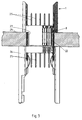
- Fig. 3 is a cross section of the connector of fig. 1 mounted on a printed circuit board.
- Fig. 4 shows a perspective view of a contact element with support elements of the connector of fig. 1.
-
- Fig. 1 shows a
connector 1, comprising ahousing 2 of insulating material and a plurality ofmale contact elements 3 regularly arranged in rows and columns at a given pitch in a conventional manner. Only afew contact elements 3 are shown in the drawings for the sake of clarity. Thehousing 2 is provided with a bottom 4 and twoopposite side walls 5, extending upwardly from the bottom 4. The bottom 4 andside walls 5 determine areceiving space 6 for receiving a female connector with female contact elements not shown. - In the embodiment shown, the bottom 4 of the
housing 2 has alower bottom extension 7 directed away from thereceiving space 6. Thisbottom extension 7 can be received in a slot of a printed circuit board as will be explained hereinafter. The bottom 4 is provided withcavities 8 regularly arranged in rows and columns for receiving thecontact elements 3. Thecavities 8 extend through the complete bottom 4 withextension 7. Thecavities 8 are metallized at theirinner walls 9, in that thecomplete housing 2 is metallized in the embodiment described. Thecontact elements 3 are mounted in themetallized cavities 8 by means of twosupport elements first support element 10 is arranged near thereceiving space 6 and thesecond support element 11 is arranged near the lower end of theextension 7. In this manner a very stable support of thecontact elements 3 within theircavities 8 is guaranteed. - As shown at a larger scale in fig. 2 and 4, each
support element body 12 with a plurality ofledges 13 extending in axial direction of thecontact element 3. The dimensions of thebody 12 of asupport element cavity 8 are such that thebodies 12 can always be received with play within thecavity 8 despite any tolerances. The outer dimension determined by theledges 13 is such that only theseledges 13 are clampingly received within thecavity 8, thereby providing an accurate mounting of thecontact elements 3 within thecavities 8. - In the embodiment shown in fig. 1-3, each
metallized cavity 8 has anupper section 14 near thereceiving space 6 having a smaller inner dimension than theremaining part 15 of thecavity 8. Theledges 13 of thefirst support element 10 determine a dimension which is smaller than the inner dimension of thepart 15 of thecavity 8, so that during manufacturing thefirst support element 10 can pass with play through thispart 15 of the cavity. However this dimension determined by theledges 13 of thefirst support element 10 is larger than the inner dimension of theupper section 14 so that thesupport element 10 is clamped within this upper section. Theledges 13 of thesecond support element 11 determine a dimension which is larger than the inner dimension of theremaining part 15 of thecavity 8, so that thesecond support element 11 is also clamped within thisremaining part 15. - The
first support element 10 of thecontact elements 3 is provided with ahead part 16 for locking thecontact element 3 within thecavity 8. The locking action is obtained by providing thehead part 16 withslots 17 at opposite sides and by providingledges 18 at opposite sides protruding into thecavity 8 at theupper section 14 near thereceiving space 6. To facilitate mounting of thecontact elements 3 within thecavities 8, thehead part 16 is provided withoblique faces 19 extending outwardly and downwardly from near thecontact pin 3 towards theslots 17. Thehead part 16 co-operating with the ledges 18 and thesupport elements ledges 13 provide for a very stable mounting of thecontact elements 3 within thecavities 8. - The described way of mounting the
contact elements 3 has the advantage that the forces exerted on the contact elements can be determined in a defined manner and the forces exerted during mounting of a conventional shroud will be received mainly by the head part of the support elements. - In the embodiment of fig. 1-3 all
cavities 8 are made as coax cavities, i.e. eachcavity 8 receives onecontact element 3. In an alternative embodiment not shown some cavities can be made as twinax cavities, i.e. cavities receiving twocontact elements 3. In such a case each column of cavities may include two twinax cavities at each side of a center cavity receiving onecontact element 3. Of course other arrangements of cavities are possible. - In the embodiment shown, a row of
cavities 21 is provided at each side of the rows ofmetallized cavities 8, whichcavities 21 are made as standard cavities for receivingstandard contact elements 22 as shown in fig. 3. Thesecontact elements 22 are used as ground contact elements which contact the metallization of thecavities 21 and are provided with press-fit sections 23 for connection to a printedcircuit board 24. The press-fit sections 23 of thecontact elements 22 further provide for a mounting of theconnector 1 on the printedcircuit board 24. - All
contact elements male contact sections 25 at their upper and lower sides, wherein aconventional shroud 26 is mounted on thecontact sections 25 opposite of thereceiving space 6. Thebottom extension 7 is received within aslot 27 in the printedcircuit board 24. - It will be understood that the
connector 1 can also be made without thebottom extension 7 and in such an embodiment afirst support element 10 will be sufficient for mounting thecontact elements 3 within thecavities 8. It is further noted that instead ofmale contact sections 25 at the side opposite of thereceiving space 6, thecontact elements - From the foregoing it will be understood, that the connector described shows the advantage that an accurate and stable mounting of the
contact elements 3 within thecavities 8, 20 is possible without the requirement of high tolerances for thecavities 8 andsupport elements contact elements 3 by themetallized cavities 8, 20 is obtained, so that all contact elements can be used as signal contact elements resulting in a high signal density. Theconnector 1 can be used in an interchangeable manner within existing connector families as the connector can be manufactured with the same dimensions and same pitch of contact elements as conventional connectors. - The invention is not restricted to above described embodiments which can be varied in a number of ways within the scope of the claims.
Claims (12)
- Connector for high frequency signals, comprising a housing of insulating material and a plurality of male contact elements, said housing having a bottom and two opposite side walls extending upwardly from the bottom, the bottom and side walls determining a receiving space, wherein the bottom is provided with cavities regularly arranged in rows and columns, wherein each of the contact elements is mounted in a cavity, an upper end of each contact element projecting into the receiving space, characterized in that at least a plurality of the cavities are metallized at their the inner walls, wherein the contact elements are mounted in the metallized cavities by means of at least one support element of insulating material, wherein each support element comprises a body having an outer dimension which is smaller than the inner dimension of the corresponding cavity, and a plurality of ledges extending mainly in axial direction of the contact element and determining an outer dimension which is larger than the inner dimension of the corresponding cavity.
- Connector according to claim 1, wherein the bottom of the housing has a lower bottom extension directed away from the receiving space, wherein said metallized cavities extend through the bottom extension, and wherein each contact element is mounted in a metallized cavity by means of at least two support elements, a first support element being arranged near the receiving space and a second support element being arranged near the lower end of the extension.
- Connector according to claim 2, wherein each metallized cavity has an upper section near the receiving space, said upper section having a smaller inner dimension than the remaining part of the cavity, wherein the ledges of the first support element determine a dimension which is smaller than the inner dimension of said remaining part and larger than the inner dimension of said upper section, wherein the ledges of the second support element determine a dimension which is larger than the inner dimension of said remaining part.
- Connector according to any one of the preceding claims, wherein the inner wall of each cavity and said at least one support element of the corresponding contact element are provided with cooperating locking means for locking the contact element in the cavity.
- Connector according to claim 2 and 4, wherein each first support element and the corresponding cavity are provided with cooperating locking means.
- Connector according to claim 4 or 5, wherein the inner wall of each metallized cavity is provided with two opposite protruding ledges and each corresponding support element is provided with a head part having slots at opposite sides for receiving the ledges.
- Connector according to claim 6, wherein the head part is provided with oblique faces extending outwardly and downwardly from the contact pin towards said slots.
- Connector according to any one of the preceding claims, wherein each support element is fixed to the corresponding contact element, preferably by overmoulding.
- Connector according to any one of the preceding claims, wherein the housing is completely metallized.
- Connector according to any one of the preceding claims, wherein at least some of said metalized cavities are provided with two contact elements.
- Connector according to any one of the preceding claims, wherein a row of cavities is provided at each side of the rows of metallized cavities, wherein male ground contact elements are mounted in the cavities of these rows, said ground contact elements contacting the metallization in the corresponding cavities and having terminals for connection to a printed circuit board.
- Connector according to claim 11, wherein said terminals of the ground contact elements are made as press-fit terminals.
Applications Claiming Priority (2)
| Application Number | Priority Date | Filing Date | Title |
|---|---|---|---|
| NL1009529A NL1009529C2 (en) | 1998-06-30 | 1998-06-30 | Connector. |
| NL1009529 | 1998-06-30 |
Publications (1)
| Publication Number | Publication Date |
|---|---|
| EP0969565A1 true EP0969565A1 (en) | 2000-01-05 |
Family
ID=19767401
Family Applications (1)
| Application Number | Title | Priority Date | Filing Date |
|---|---|---|---|
| EP99202031A Withdrawn EP0969565A1 (en) | 1998-06-30 | 1999-06-24 | Connector |
Country Status (3)
| Country | Link |
|---|---|
| US (1) | US6159048A (en) |
| EP (1) | EP0969565A1 (en) |
| NL (1) | NL1009529C2 (en) |
Cited By (2)
| Publication number | Priority date | Publication date | Assignee | Title |
|---|---|---|---|---|
| FR2810800A1 (en) * | 2000-06-23 | 2001-12-28 | Alstom | FEMALE PART OF A TWO-PART CONNECTOR AND CONTACT FOR EQUIPPING THIS FEMALE PART |
| WO2013079059A1 (en) * | 2011-11-28 | 2013-06-06 | Harting Kgaa | Insulating body of a plug-in connector |
Families Citing this family (6)
| Publication number | Priority date | Publication date | Assignee | Title |
|---|---|---|---|---|
| US6695627B2 (en) * | 2001-08-02 | 2004-02-24 | Fci Americas Technnology, Inc. | Profiled header ground pin |
| JP2006515705A (en) * | 2002-05-06 | 2006-06-01 | モレックス インコーポレーテッド | Differential signal connector with electrostatic discharge protection function |
| DE102005012369A1 (en) * | 2005-03-09 | 2006-09-14 | Adc Gmbh | Junction box for a data network |
| DE102005012370B3 (en) * | 2005-03-09 | 2006-06-01 | Adc Gmbh | Pressure module for locking a bush in a connecting socket has cable fixing element of metal or metallized plastic on which spring acts |
| WO2011090632A2 (en) * | 2009-12-30 | 2011-07-28 | Fci | Electrical connector having conductive housing |
| EP2518835B1 (en) * | 2011-04-28 | 2019-01-16 | Harman Becker Automotive Systems GmbH | Electrical connector |
Citations (5)
| Publication number | Priority date | Publication date | Assignee | Title |
|---|---|---|---|---|
| GB967325A (en) * | 1960-12-06 | 1964-08-19 | Alex Just | Electrical terminal connectors |
| US3774142A (en) * | 1972-05-10 | 1973-11-20 | Elco Corp | Sleeve for grounding bushing-mounted contact to plate |
| FR2693845A1 (en) * | 1992-07-17 | 1994-01-21 | Air Lb International Sa | Screened electric connector for electrical conductors - uses casing made in two parts of metal plated plastic, with one part being lipped to ensure tight fit and good earth contact between both parts |
| EP0693795A1 (en) * | 1994-07-22 | 1996-01-24 | Connector Systems Technology N.V. | Selectively metallizized connector with at least one coaxial or twinaxial terminal |
| US5647768A (en) * | 1996-03-11 | 1997-07-15 | General Motors Corporation | Plated plastic filter header |
Family Cites Families (11)
| Publication number | Priority date | Publication date | Assignee | Title |
|---|---|---|---|---|
| US3721869A (en) * | 1971-11-22 | 1973-03-20 | Hubbell Inc Harvey | Filter contact connector assembly with contact pins having integrally constructed capacitors |
| US4451107A (en) * | 1982-08-23 | 1984-05-29 | Amp Incorporated | High speed modular connector for printed circuit boards |
| US5261829A (en) * | 1990-06-08 | 1993-11-16 | Fusselman David F | Connectors with ground structure |
| GB9205088D0 (en) * | 1992-03-09 | 1992-04-22 | Amp Holland | Shielded back plane connector |
| GB9205087D0 (en) * | 1992-03-09 | 1992-04-22 | Amp Holland | Sheilded back plane connector |
| US5417588A (en) * | 1993-11-15 | 1995-05-23 | Adc Telecommunications, Inc. | Coax connector with center pin locking |
| DE4341104C1 (en) * | 1993-12-02 | 1995-01-12 | Harting Elektronik Gmbh | Screened printed circuit board plug connection |
| EP0677895A3 (en) * | 1994-04-14 | 1996-09-11 | Siemens Ag | Connector for rear panels. |
| EP0680117A3 (en) * | 1994-04-29 | 1997-03-26 | Siemens Ag | Plug connection between backplane circuit boards and assembly circuit boards. |
| DE19511507A1 (en) * | 1995-03-29 | 1996-10-02 | Siemens Ag | Electrical connector |
| US5980271A (en) * | 1998-04-15 | 1999-11-09 | Hon Hai Precision Ind. Co., Ltd. | Header connector of a future bus and related compliant pins |
-
1998
- 1998-06-30 NL NL1009529A patent/NL1009529C2/en not_active IP Right Cessation
-
1999
- 1999-06-24 US US09/339,766 patent/US6159048A/en not_active Expired - Fee Related
- 1999-06-24 EP EP99202031A patent/EP0969565A1/en not_active Withdrawn
Patent Citations (5)
| Publication number | Priority date | Publication date | Assignee | Title |
|---|---|---|---|---|
| GB967325A (en) * | 1960-12-06 | 1964-08-19 | Alex Just | Electrical terminal connectors |
| US3774142A (en) * | 1972-05-10 | 1973-11-20 | Elco Corp | Sleeve for grounding bushing-mounted contact to plate |
| FR2693845A1 (en) * | 1992-07-17 | 1994-01-21 | Air Lb International Sa | Screened electric connector for electrical conductors - uses casing made in two parts of metal plated plastic, with one part being lipped to ensure tight fit and good earth contact between both parts |
| EP0693795A1 (en) * | 1994-07-22 | 1996-01-24 | Connector Systems Technology N.V. | Selectively metallizized connector with at least one coaxial or twinaxial terminal |
| US5647768A (en) * | 1996-03-11 | 1997-07-15 | General Motors Corporation | Plated plastic filter header |
Cited By (3)
| Publication number | Priority date | Publication date | Assignee | Title |
|---|---|---|---|---|
| FR2810800A1 (en) * | 2000-06-23 | 2001-12-28 | Alstom | FEMALE PART OF A TWO-PART CONNECTOR AND CONTACT FOR EQUIPPING THIS FEMALE PART |
| EP1168517A1 (en) * | 2000-06-23 | 2002-01-02 | Alstom | Female part of a two-part connector and contact for this female part |
| WO2013079059A1 (en) * | 2011-11-28 | 2013-06-06 | Harting Kgaa | Insulating body of a plug-in connector |
Also Published As
| Publication number | Publication date |
|---|---|
| NL1009529C2 (en) | 2000-01-04 |
| US6159048A (en) | 2000-12-12 |
Similar Documents
| Publication | Publication Date | Title |
|---|---|---|
| US6299484B2 (en) | Shielded connector | |
| EP0620616B1 (en) | Connector for coaxial and/or twinaxial cables | |
| EP0670616B1 (en) | Connector for a cable for high frequency signals | |
| US6719587B2 (en) | Right-angled connector | |
| EP0446980B2 (en) | Connector assembly for printed circuit boards | |
| US6695622B2 (en) | Electrical system having means for accommodating various distances between PC boards thereof mounting the means | |
| US5775947A (en) | Multi-contact connector with cross-talk blocking elements between signal contacts | |
| JP3194216B2 (en) | Electrical connector | |
| US6648657B1 (en) | Electrical connector having ground buses | |
| US6425766B1 (en) | Impedance control in edge card connector systems | |
| JPH04272676A (en) | Electric connector | |
| US20020160632A1 (en) | Low pitch, high density connector | |
| US6056559A (en) | Punched sheet coax header | |
| US6123584A (en) | Connector | |
| US6159048A (en) | Connector for high frequency signals | |
| US7101225B2 (en) | Shielded high-density edge connector | |
| US20010003077A1 (en) | Shielded connector assembly | |
| US5236368A (en) | Printed circuit board and outrigger edge connector assembly and method of assembling the same | |
| US6375507B1 (en) | Connector and method for manufacturing a connector | |
| US6802732B1 (en) | Card edge connector | |
| US6851981B2 (en) | Terminal block with ground contact for connecting to adjacent terminal block | |
| US6579124B1 (en) | Shielded electrical connector | |
| EP0374307A1 (en) | Connector assembly for printed circuit boards | |
| EP0891018B1 (en) | Connector | |
| US6220868B1 (en) | Card edge connector |
Legal Events
| Date | Code | Title | Description |
|---|---|---|---|
| PUAI | Public reference made under article 153(3) epc to a published international application that has entered the european phase |
Free format text: ORIGINAL CODE: 0009012 |
|
| AK | Designated contracting states |
Kind code of ref document: A1 Designated state(s): BE DE FR GB NL SE |
|
| AX | Request for extension of the european patent |
Free format text: AL;LT;LV;MK;RO;SI |
|
| 17P | Request for examination filed |
Effective date: 20000613 |
|
| AKX | Designation fees paid |
Free format text: BE DE FR GB NL SE |
|
| GRAP | Despatch of communication of intention to grant a patent |
Free format text: ORIGINAL CODE: EPIDOSNIGR1 |
|
| STAA | Information on the status of an ep patent application or granted ep patent |
Free format text: STATUS: THE APPLICATION IS DEEMED TO BE WITHDRAWN |
|
| 18D | Application deemed to be withdrawn |
Effective date: 20080327 |