EP0962987B1 - Vertical trench-gate power MOSFET having stripe geometry and high cell density - Google Patents
Vertical trench-gate power MOSFET having stripe geometry and high cell density Download PDFInfo
- Publication number
- EP0962987B1 EP0962987B1 EP99110268A EP99110268A EP0962987B1 EP 0962987 B1 EP0962987 B1 EP 0962987B1 EP 99110268 A EP99110268 A EP 99110268A EP 99110268 A EP99110268 A EP 99110268A EP 0962987 B1 EP0962987 B1 EP 0962987B1
- Authority
- EP
- European Patent Office
- Prior art keywords
- cell
- region
- mosfet
- power mosfet
- cells
- Prior art date
- Legal status (The legal status is an assumption and is not a legal conclusion. Google has not performed a legal analysis and makes no representation as to the accuracy of the status listed.)
- Expired - Lifetime
Links
- 210000000746 body region Anatomy 0.000 claims description 12
- 239000002019 doping agent Substances 0.000 claims description 12
- 239000004065 semiconductor Substances 0.000 claims description 4
- 230000001681 protective effect Effects 0.000 claims description 3
- 230000003252 repetitive effect Effects 0.000 claims description 2
- 238000009792 diffusion process Methods 0.000 description 15
- 229910052751 metal Inorganic materials 0.000 description 14
- 239000002184 metal Substances 0.000 description 14
- 238000000034 method Methods 0.000 description 11
- 239000007943 implant Substances 0.000 description 6
- 229910021420 polycrystalline silicon Inorganic materials 0.000 description 5
- 229920005591 polysilicon Polymers 0.000 description 5
- ZOXJGFHDIHLPTG-UHFFFAOYSA-N Boron Chemical compound [B] ZOXJGFHDIHLPTG-UHFFFAOYSA-N 0.000 description 4
- 229910052796 boron Inorganic materials 0.000 description 4
- 238000005468 ion implantation Methods 0.000 description 4
- 230000003071 parasitic effect Effects 0.000 description 4
- 229910052698 phosphorus Inorganic materials 0.000 description 4
- 239000000758 substrate Substances 0.000 description 4
- OAICVXFJPJFONN-UHFFFAOYSA-N Phosphorus Chemical compound [P] OAICVXFJPJFONN-UHFFFAOYSA-N 0.000 description 3
- 230000015556 catabolic process Effects 0.000 description 3
- 239000011574 phosphorus Substances 0.000 description 3
- 230000015572 biosynthetic process Effects 0.000 description 2
- 230000000694 effects Effects 0.000 description 2
- 238000004519 manufacturing process Methods 0.000 description 2
- 230000000737 periodic effect Effects 0.000 description 2
- XHXFXVLFKHQFAL-UHFFFAOYSA-N phosphoryl trichloride Chemical compound ClP(Cl)(Cl)=O XHXFXVLFKHQFAL-UHFFFAOYSA-N 0.000 description 2
- 229910019213 POCl3 Inorganic materials 0.000 description 1
- 230000002411 adverse Effects 0.000 description 1
- 229910052785 arsenic Inorganic materials 0.000 description 1
- RQNWIZPPADIBDY-UHFFFAOYSA-N arsenic atom Chemical compound [As] RQNWIZPPADIBDY-UHFFFAOYSA-N 0.000 description 1
- 230000002457 bidirectional effect Effects 0.000 description 1
- 230000000903 blocking effect Effects 0.000 description 1
- 239000005380 borophosphosilicate glass Substances 0.000 description 1
- 239000000969 carrier Substances 0.000 description 1
- 239000013078 crystal Substances 0.000 description 1
- 230000007423 decrease Effects 0.000 description 1
- 230000001419 dependent effect Effects 0.000 description 1
- 239000010432 diamond Substances 0.000 description 1
- 238000001312 dry etching Methods 0.000 description 1
- 230000005684 electric field Effects 0.000 description 1
- 238000005516 engineering process Methods 0.000 description 1
- 230000005669 field effect Effects 0.000 description 1
- 239000000463 material Substances 0.000 description 1
- 230000009467 reduction Effects 0.000 description 1
- 238000004088 simulation Methods 0.000 description 1
Images


Classifications
-
- H—ELECTRICITY
- H01—ELECTRIC ELEMENTS
- H01L—SEMICONDUCTOR DEVICES NOT COVERED BY CLASS H10
- H01L29/00—Semiconductor devices adapted for rectifying, amplifying, oscillating or switching, or capacitors or resistors with at least one potential-jump barrier or surface barrier, e.g. PN junction depletion layer or carrier concentration layer; Details of semiconductor bodies or of electrodes thereof ; Multistep manufacturing processes therefor
- H01L29/66—Types of semiconductor device ; Multistep manufacturing processes therefor
- H01L29/68—Types of semiconductor device ; Multistep manufacturing processes therefor controllable by only the electric current supplied, or only the electric potential applied, to an electrode which does not carry the current to be rectified, amplified or switched
- H01L29/76—Unipolar devices, e.g. field effect transistors
- H01L29/772—Field effect transistors
- H01L29/78—Field effect transistors with field effect produced by an insulated gate
- H01L29/7801—DMOS transistors, i.e. MISFETs with a channel accommodating body or base region adjoining a drain drift region
- H01L29/7802—Vertical DMOS transistors, i.e. VDMOS transistors
- H01L29/7813—Vertical DMOS transistors, i.e. VDMOS transistors with trench gate electrode, e.g. UMOS transistors
-
- H—ELECTRICITY
- H01—ELECTRIC ELEMENTS
- H01L—SEMICONDUCTOR DEVICES NOT COVERED BY CLASS H10
- H01L27/00—Devices consisting of a plurality of semiconductor or other solid-state components formed in or on a common substrate
- H01L27/02—Devices consisting of a plurality of semiconductor or other solid-state components formed in or on a common substrate including semiconductor components specially adapted for rectifying, oscillating, amplifying or switching and having at least one potential-jump barrier or surface barrier; including integrated passive circuit elements with at least one potential-jump barrier or surface barrier
- H01L27/0203—Particular design considerations for integrated circuits
- H01L27/0248—Particular design considerations for integrated circuits for electrical or thermal protection, e.g. electrostatic discharge [ESD] protection
- H01L27/0251—Particular design considerations for integrated circuits for electrical or thermal protection, e.g. electrostatic discharge [ESD] protection for MOS devices
- H01L27/0255—Particular design considerations for integrated circuits for electrical or thermal protection, e.g. electrostatic discharge [ESD] protection for MOS devices using diodes as protective elements
-
- H—ELECTRICITY
- H01—ELECTRIC ELEMENTS
- H01L—SEMICONDUCTOR DEVICES NOT COVERED BY CLASS H10
- H01L27/00—Devices consisting of a plurality of semiconductor or other solid-state components formed in or on a common substrate
- H01L27/02—Devices consisting of a plurality of semiconductor or other solid-state components formed in or on a common substrate including semiconductor components specially adapted for rectifying, oscillating, amplifying or switching and having at least one potential-jump barrier or surface barrier; including integrated passive circuit elements with at least one potential-jump barrier or surface barrier
- H01L27/04—Devices consisting of a plurality of semiconductor or other solid-state components formed in or on a common substrate including semiconductor components specially adapted for rectifying, oscillating, amplifying or switching and having at least one potential-jump barrier or surface barrier; including integrated passive circuit elements with at least one potential-jump barrier or surface barrier the substrate being a semiconductor body
- H01L27/06—Devices consisting of a plurality of semiconductor or other solid-state components formed in or on a common substrate including semiconductor components specially adapted for rectifying, oscillating, amplifying or switching and having at least one potential-jump barrier or surface barrier; including integrated passive circuit elements with at least one potential-jump barrier or surface barrier the substrate being a semiconductor body including a plurality of individual components in a non-repetitive configuration
- H01L27/07—Devices consisting of a plurality of semiconductor or other solid-state components formed in or on a common substrate including semiconductor components specially adapted for rectifying, oscillating, amplifying or switching and having at least one potential-jump barrier or surface barrier; including integrated passive circuit elements with at least one potential-jump barrier or surface barrier the substrate being a semiconductor body including a plurality of individual components in a non-repetitive configuration the components having an active region in common
- H01L27/0705—Devices consisting of a plurality of semiconductor or other solid-state components formed in or on a common substrate including semiconductor components specially adapted for rectifying, oscillating, amplifying or switching and having at least one potential-jump barrier or surface barrier; including integrated passive circuit elements with at least one potential-jump barrier or surface barrier the substrate being a semiconductor body including a plurality of individual components in a non-repetitive configuration the components having an active region in common comprising components of the field effect type
- H01L27/0727—Devices consisting of a plurality of semiconductor or other solid-state components formed in or on a common substrate including semiconductor components specially adapted for rectifying, oscillating, amplifying or switching and having at least one potential-jump barrier or surface barrier; including integrated passive circuit elements with at least one potential-jump barrier or surface barrier the substrate being a semiconductor body including a plurality of individual components in a non-repetitive configuration the components having an active region in common comprising components of the field effect type in combination with diodes, or capacitors or resistors
-
- H—ELECTRICITY
- H01—ELECTRIC ELEMENTS
- H01L—SEMICONDUCTOR DEVICES NOT COVERED BY CLASS H10
- H01L29/00—Semiconductor devices adapted for rectifying, amplifying, oscillating or switching, or capacitors or resistors with at least one potential-jump barrier or surface barrier, e.g. PN junction depletion layer or carrier concentration layer; Details of semiconductor bodies or of electrodes thereof ; Multistep manufacturing processes therefor
- H01L29/02—Semiconductor bodies ; Multistep manufacturing processes therefor
- H01L29/06—Semiconductor bodies ; Multistep manufacturing processes therefor characterised by their shape; characterised by the shapes, relative sizes, or dispositions of the semiconductor regions ; characterised by the concentration or distribution of impurities within semiconductor regions
- H01L29/0684—Semiconductor bodies ; Multistep manufacturing processes therefor characterised by their shape; characterised by the shapes, relative sizes, or dispositions of the semiconductor regions ; characterised by the concentration or distribution of impurities within semiconductor regions characterised by the shape, relative sizes or dispositions of the semiconductor regions or junctions between the regions
- H01L29/0692—Surface layout
- H01L29/0696—Surface layout of cellular field-effect devices, e.g. multicellular DMOS transistors or IGBTs
-
- H—ELECTRICITY
- H01—ELECTRIC ELEMENTS
- H01L—SEMICONDUCTOR DEVICES NOT COVERED BY CLASS H10
- H01L29/00—Semiconductor devices adapted for rectifying, amplifying, oscillating or switching, or capacitors or resistors with at least one potential-jump barrier or surface barrier, e.g. PN junction depletion layer or carrier concentration layer; Details of semiconductor bodies or of electrodes thereof ; Multistep manufacturing processes therefor
- H01L29/02—Semiconductor bodies ; Multistep manufacturing processes therefor
- H01L29/06—Semiconductor bodies ; Multistep manufacturing processes therefor characterised by their shape; characterised by the shapes, relative sizes, or dispositions of the semiconductor regions ; characterised by the concentration or distribution of impurities within semiconductor regions
- H01L29/10—Semiconductor bodies ; Multistep manufacturing processes therefor characterised by their shape; characterised by the shapes, relative sizes, or dispositions of the semiconductor regions ; characterised by the concentration or distribution of impurities within semiconductor regions with semiconductor regions connected to an electrode not carrying current to be rectified, amplified or switched and such electrode being part of a semiconductor device which comprises three or more electrodes
- H01L29/1095—Body region, i.e. base region, of DMOS transistors or IGBTs
-
- H—ELECTRICITY
- H01—ELECTRIC ELEMENTS
- H01L—SEMICONDUCTOR DEVICES NOT COVERED BY CLASS H10
- H01L29/00—Semiconductor devices adapted for rectifying, amplifying, oscillating or switching, or capacitors or resistors with at least one potential-jump barrier or surface barrier, e.g. PN junction depletion layer or carrier concentration layer; Details of semiconductor bodies or of electrodes thereof ; Multistep manufacturing processes therefor
- H01L29/66—Types of semiconductor device ; Multistep manufacturing processes therefor
- H01L29/68—Types of semiconductor device ; Multistep manufacturing processes therefor controllable by only the electric current supplied, or only the electric potential applied, to an electrode which does not carry the current to be rectified, amplified or switched
- H01L29/76—Unipolar devices, e.g. field effect transistors
- H01L29/772—Field effect transistors
- H01L29/78—Field effect transistors with field effect produced by an insulated gate
- H01L29/7801—DMOS transistors, i.e. MISFETs with a channel accommodating body or base region adjoining a drain drift region
- H01L29/7802—Vertical DMOS transistors, i.e. VDMOS transistors
- H01L29/7803—Vertical DMOS transistors, i.e. VDMOS transistors structurally associated with at least one other device
- H01L29/7808—Vertical DMOS transistors, i.e. VDMOS transistors structurally associated with at least one other device the other device being a breakdown diode, e.g. Zener diode
-
- H—ELECTRICITY
- H01—ELECTRIC ELEMENTS
- H01L—SEMICONDUCTOR DEVICES NOT COVERED BY CLASS H10
- H01L29/00—Semiconductor devices adapted for rectifying, amplifying, oscillating or switching, or capacitors or resistors with at least one potential-jump barrier or surface barrier, e.g. PN junction depletion layer or carrier concentration layer; Details of semiconductor bodies or of electrodes thereof ; Multistep manufacturing processes therefor
- H01L29/66—Types of semiconductor device ; Multistep manufacturing processes therefor
- H01L29/68—Types of semiconductor device ; Multistep manufacturing processes therefor controllable by only the electric current supplied, or only the electric potential applied, to an electrode which does not carry the current to be rectified, amplified or switched
- H01L29/76—Unipolar devices, e.g. field effect transistors
- H01L29/772—Field effect transistors
- H01L29/78—Field effect transistors with field effect produced by an insulated gate
- H01L29/7827—Vertical transistors
Definitions
- a power MOSFET is typically formed in a geometric pattern of cells.
- the cells may be in the shape of a closed figure such as a square or hexagon or they may comprise a series of parallel longitudinal stripes.
- the cell is defined at its perimeter by the gate electrode, and the interior of each cell normally contains a source diffusion and a body diffusion.
- a single drain is normally located on the opposite side of the chip from the source and body and thus underlies the cells.
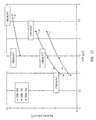
- Figs 1A, 1B and 1C illustrate overhead views of a single cell of a trench-gated MOSFET in a square, hexagonal and stripe configuration, respectively.
- the outermost region represents one-half of the trenched gate (the other half belonging to the adjacent cell)
- the middle region represents the source region
- the innermost region represents the body contact region.
- the body region is in effect a continuation of the body contact region and extends under the source region to the sidewall of the trench, where the channel is located.
- the hatched regions represent the overlying metal source contact which in many power MOSFETs also contacts the body region to prevent the parasitic bipolar transistor from turning on.
- each cell is defined by Ysb, which is the width of the source and body regions, i.e., the mesa inside the gate trench, and Yg, which is the width of the gate. As indicated, one-half of Yg is located on each side of the source/body region.
- the overall width or pitch of the cell is equal to Ysb + Yg.
- EP 0746042A2 discloses a bidirectional blocking trench power MOSFET.
- EP 0755076A2 discloses a vertical MOS semiconductor with recessed gate and method of manufacturing the same.
- Non-prepublished EP 0923137A2 discloses a trenched field effect transistor and method of its manufacture.
- a figure of merit for a power MOSFET is the area/perimeter ratio or A/W, which is amount of area that is required to provide a given channel width.
- A/W area/perimeter ratio
- the area and channel width (measured horizontally along the wall of the trench), and the resulting value of A/W, can be calculated for each of cells shown in Figs. 1A, 1B and 1C .
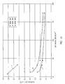
- Fig. 2 is a graph showing A/W as a function of cell density for three types of cells.
- Curve A represents A/W for a striped cell
- curve B represents A/W for a square cell having a gate width Yg of 1 ⁇ m
- curve C represent A/W for a square cell having a gate width of 0.65 ⁇ m.
- the cell density which is measured in millions of cells per square inch, is intended to be a measure of the cell dimension that must be defined by photolithographic processes.
- the density of the striped cells in order to be equivalent to the density of the square cells, is figured on the basis of the number of square cells having a side dimension equal to the width of the stripe that would occupy 6.45 cm 2 (a square inch).
- the corresponding cell pitch is shown at the top of the graph, a pitch of about 4.5 ⁇ m corresponding, for example, to a cell density of 4.96 Mcells/cm 2 (32 Mcells/in 2 ).
- this limit arises because of the necessity of forming a body contact region within each cell to avoid parasitic bipolar turn-on, as shown in Figs. 1A-1C .
- Another cause is the need to form a deep diffusion within each cell, as taught in U.S. Patent No. 5,072,266 to Bulucea et al ., to protect the gate oxide layer. In conjuction, these factors place a lower limit on the lateral dimension of each cell and hence the cell density.
- a trench-gated power MOSFET having a cell density as high as 27.6 Mcells/cm 2 (178 Mcells/in 2 ) is fabricated, using a striped cell geometry. As indicated in Fig. 2 , this requires that the cell pitch be about 1.9 ⁇ m.
- This reduced cell pitch is obtained by providing a power MOSFET in accordance with the present invention, as set out in claim 1. Specific embodiments are defined in the dependent claims.
- Body contact regions are formed at both ends of the stripe ; in embodiments body contact regions are further formed at intervals along the stripe to limit resistive losses and consequent voltage drops from occurring between the source and body in portions of the striped cell.
- the gate oxide layer may be protected by forming a deep diffusion at periodic intervals throughout the cell lattice, as taught in U.S. Patent No. 5,998,837 .
- the cell pitch can be reduced to about 1.9 ⁇ m, thereby reducing the area/perimeter ratio by a factor on the order of 36%.
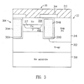
- MOSFET cell 30 is formed on an N-type epitaxial (epi) layer 302, which is grown on an N+ substrate 300.
- Cell 30 is stripe-shaped and is defined on two sides by opposing gate sections 304A and 304B which are positioned within trenches formed at the top surface of N-epi layer 302.
- Sections 304A and 304B are two sections of a gate 304 which contains a plurality of similar gate sections arranged in a parallel array to form a corresponding plurality of parallel striped cells.
- Gate sections 304A and 304B are electrically isolated from N-epi layer 302 by gate oxide layers 306A and 306B, respectively.
- Gate sections 304A and 304B are electrically tied together at some location on the MOSFET.
- the polysilicon layer that is normally used to form gate 304 can be patterned in such a way that the parallel gate sections merge in some region.
- Generally cell 30 has a length dimension parallel to gate sections 304A and 304B that is at least ten times its width dimension perpendicular to gate sections 304A and 304B.
- Fig. 17 shows a top view of a power MOSFET chip which contains three rows of stripe MOSFET cells. Each row would typically contain thousands of cells.
- Cell 30 contains an N+ source region 308 and a P-body 310. Electrical contact is made with N+ source region 308 by means of a metal layer 312 through an opening in an oxide layer 314. Oxide layer 314 generally overlies the gate sections 304A and 304B but extends some distance over N+ source region 308 to insure that metal layer 312 does not come into contact with gate sections 304A and 304B. Shorting the gate to the source would disable the MOSFET.
- the MOSFET when the MOSFET is turned on current flows vertically between the metal layer 312 and a drain contact (not shown) that is formed at the bottom of the N+ substrate 300.
- the path of the current runs through the N+ source region 308, the P-body 312, the N-epi layer 302 and the N+ substrate 300.
- the current flows through a channel region located adjacent the trench in the P-body, and the flow of current through the channel region can be interrupted by biasing the gate 304 appropriately so as to turn the MOSFET off.
- Deep P+ diffusion 316 forms a PN junction with the N-type material in the N-epi layer 302. This PN junction functions as a diode.
- Metal layer 312 ties the deep P+ diffusion 316 (i.e., one terminal of the diode) to N+ source region 308 of MOSFET cell 30 such that the diode is connected in parallel with the channel of the MOSFET cell.
- Deep P+ diffusion 316 operates to reduce the strength of the electric field across the gate oxide layers 306A, 306B and at the corners of the trenches and limits the formation of hot carriers in the vicinity of the trench.
- the diode also operates as a voltage clamp and thereby limits the voltage across the gate oxide layer. While the PN junction in diode cell 32 is shown as being below the bottom of the trench, this need not be the case so long as the diode breaks down before the MOSFET cell 30
- one protective diode cell is provided for a selected number of MOSFET cells in a repetitive pattern across the MOSFET.
- the number of diode cells per MOSFET cells is determined by the design criteria of the MOSFET. In general, for example, MOSFETs which are expected to experience breakdown more often will require a greater proportion of diode cells.
- Figs. 6 and 7 show top views of MOSFETs 60 and 70, respectively, each of which contains two MOSFET cells 62, 72 for each diode cell 64, 74.
- the numerals 66A-66D and 76A-76D designate sections of the gates of MOSFETs 60 and 70.
- Diode cell 64 occupies the entire region between gate sections 66C and 66D whereas diode cell 74 is interrupted in a portion of the region between gate sections 76C and 76D to allow an additional MOSFET cell 78 to be formed.
- MOSFET cell 30 also contains a P+ region 317 immediately below N+ source region 308.
- the dopant concentration of P+ region 317 is in the range of 5 x 10 18 to 8 x 10 19 cm -3 (preferably about 3-4 x 10 19 cm -3 ), as compared to a dopant concentration in the range of 8 x 10 15 to 7 x 10 17 cm -3 for P-body 310 generally.
- P+ region 317 does not reach the surface of epi layer 302 in the plane of Fig. 3 . Instead the contact to P+ region 317 is made as shown in Fig.
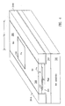
- FIG. 4 is a perspective view of MOSFET 30 without metal layer 312 and oxide layer 314 (as is apparent, Figs. 3 and 4 are drawn to a different scale).
- P+ region 317 is brought to the surface of epi layer 302 in a location (316) outside the plane of Fig. 3 . This location may be at the end of the stripe cell, or as shown in Fig. 6 , there can be a series of P+ contact regions in a ladder arrangement along the stripe cell.
- a metal layer is deposited over the structure, along with oxide layers over the trenches as shown in Fig. 3 , the N+ source regions and P-body regions are shorted together.
- the cell pitch y sb + y g can be reduced to as low as 1.9 ⁇ m or even less, allowing a cell density of 27.6 Mcells/cm 2 (178 Mcells/in 2 ) or more.
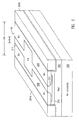
- MOSFET cell 50 is similar to MOSFET cell 30 in all respects, except that P+ region 317 is replaced by P+ region 517, which is additionally allowed to come to the surface of epi layer 302 along a thin band at the center of the cell. Since the width Yb of the band is much less than would normally be required to provide a good body contact, the presence of the thin surface band does not significantly affect the width Ysb of the mesa between gate sections 304A and 304B. As with the embodiment of Fig. 4 , the areas where the P+ body contact region is brought to the surface across the entire mesa between gate section 304A and 304B can be located at the end of the cell or periodically at intervals along the length of the cell.
- Fig. 8 shows a MOSFET cell having a pitch of 1.9 microns.
- the width of the trench (Yg) is 0.65 ⁇ m and the width of the mesa between trenches (Ysb) is 1.25 ⁇ m.
- the oxide layer overlying the gate trenches extends 0.325 ⁇ m over the mesa, leaving a width of 0.6 ⁇ m for the source/body contact.
- FIGs. 9A-9E illustrate an exemplary process for fabricating the MOSFETs shown in Figs. 3-5 .
- the starting point is the N+ substrate 300 on which the N-epitaxial layer 302 is grown using known processes.
- a thick oxide layer 930 is grown, masked and etched, and a thin oxide layer 931 is grown on the top surface of the structure where deep P+ diffusion 316 is to be formed. Deep P+ diffusion 316 is then implanted through thin oxide layer 931 at a dose of 1 x 10 14 to 7 x 10 15 cm -2 and an energy of 60-100 keV, and then driven in to a depth of from 1 to 3 ⁇ m (typically 1.5 to 2 ⁇ m). The resulting structure is illustrated in Fig. 9A . Oxide layers 930 and 931 are then removed.
- a thick oxide layer 932 is grown and removed by photomasking except over deep P+ diffusion 316, and a thin oxide layer 933 is grown.
- Thin oxide layer 933 is masked and removed from the portions of the structure where the trenches are to be formed, as shown in Fig. 9B .
- the trenches are then masked and etched using known techniques of reactive ion or plasma dry etching. Then the trench is oxidized to form gate oxide layers 306A, 306B, and polysilicon is deposited into the trench until it overflows the top of the trench.
- the polysilicon is then doped with phosphorus by POCl 3 predeposition or ion implantation at a dose of 5 x 10 13 to 5 x 10 15 cm -2 and an energy of 60 keV, giving it a sheet resistance of 20-70 ⁇ /square.
- the polysilicon is doped with boron using ion implantation to a sheet resistance of roughly 40-120 ⁇ /square.
- the polysilicon is then etched back until it is planar with the surface of the trench except where a mask protects it, so that it can subsequently be contacted with metal.
- P-body 310 is then implanted through the thin oxide layer 933 (e.g., boron at a dose of 5 x 10 12 to 9 x 10 13 cm -2 and an energy of 40-100 keV, typically 90 keV), and driven in at 1050° C for 3-10 hours to a depth of 2-3 ⁇ m.
- the thin oxide layer 933 e.g., boron at a dose of 5 x 10 12 to 9 x 10 13 cm -2 and an energy of 40-100 keV, typically 90 keV
- a similar method is used in fabricating a P-channel device except that the dopant is phosphorus.
- the resulting structure is illustrated in Fig. 9C .
- the N+ source region 34 is then introduced using a mask and an arsenic or phosphorus ion implantation (or a boron ion implantation for a P-channel device) at a dose of 1 x 10 15 to 1 x 10 16 cm -2 at 20 to 100 keV. An anneal is then performed to correct for damage to the crystal. The resulting structure is shown in Fig. 9D .
- the mask that is used during the N+ source implant covers all areas other than the intended source regions.
- the N+ source mask would cover the areas which are to be doped P+ at the surface to allow for contact to the P-body region.
- the P+ region 317 is formed underneath the N+ source region 308. This can be done by implanting boron at a high energy (e.g., 200 keV to 2 MeV) along the entire stripe so that the dopant ends up concentrated beneath the N+ source region 308.
- the dose of this implant would typically be in the range of 1 x 10 14 to 5 x 10 15 cm -2 .
- this implant can be conducted before the N+ source region 308 is formed.
- the P+ implant can conveniently be performed through the contact holes after the oxide layer 314 has been deposited over the trenches. Otherwise, a separate mask would be required for the P+ implant. This process is illustrated in Fig. 9E .
- the P+ dopant can be implanted at a much lower energy (e.g., 20 to 60 keV) before the N+ source region 308 is formed, and the P+ dopant can be driven in until it reaches the desired depth below the yet-to-be-formed N+ source region 308.
- a much lower energy e.g. 20 to 60 keV
- Metal layer 312 is deposited, forming contacts with the source and body regions and the deep P+ region through the contact holes.
- the die is then passivated with SiN or BPSG, and pad mask windows are etched to facilitate bonding.
- Fig. 11 is a detailed view of MOSFET cell 50 shown in Fig. 5 or Fig. 10C , illustrating how the P+ region 17 may be formed.
- the dashed lines 522 indicate where the edges of the mask used to form the N+ source region 308 were located.
- the letter "a” indicates the amount by which oxide layer 314 overlaps the mesa between the gate trenches. Thus, the edges of the N+ source mask were spaced a distance a + b from the trenches.
- the letter "c” indicates the lateral diffusion of the N+ source region 308 during drive-in.
- the width of the central P+ band 520 was 0.28 ⁇ m .
- the metal contact (not shown) would be 0.80 ⁇ m wide (2b + 2c + d) and the contact with the N+ source region 308 would be 0.52 ⁇ m wide (2b + 2c).
- the narrow width of the metal contact opening (0.80 ⁇ m) would require that the oxide layer 314 be kept thin enough to avoid the formation of voids when metal layer 314 is deposited.
- both the central P+ band 520 and the overlying metal layer substantially reduces the amount of the voltage drop in the body in the MOSFETs of Figs. 5 , 10C and 11 .
- a larger body voltage drop may be tolerated if the breakdown voltage of the diode cell 32 is significantly below the breakdown voltage of the MOSFET cell 30, since in that case the risk that parasitic bipolar transistor (N+ source region 308, P-body 310 and N-epi layer 302) will turn on is lessened. If so, the MOSFETs shown in Figs. 3 , 4 , 10A and 10B may be satisfactory.
- Another advantage of the MOSFET of this invention is that there is only a limited need for the channel blocks described in U.S. Patent No. 5,468,982 to prevent current leakage.
- the proportional area occupied by the channel blocks, which are located at the corners of the cells increases as the dimensions of cell are reduced. With a striped cell arrangement, the effect of the channel blocks is negligible.
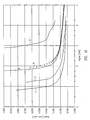
- Figs. 12-16 illustrate the advantages of a 27.6 Mcell/cm 2 (178 Mcell/in 2 ) device.
- Fig. 12 shows the specific on-resistance RonA (mohm-cm 2 ) as a function of the area/perimeter ratio.
- Curve D is for a 500A 60V device with cell densities ranging from 1.24 Mcell/cm 2 (8 Mcell/in 2 ) to 4.96 Mcell/cm 2 (32 Mcell/in 2 ).
- Curve E is for a 500A 30V device with cell densities ranging from 1.86 Mcell/cm 2 (12 Mcell/in 2 ) to 27.6 Mcell/cm 2 (178 Mcell/in 2 ).
- Curve F is for a 300A 20V device with cell densities ranging from 1.86 Mcell/cm 2 (12 Mcell/in 2 ) to 27.6 Mcell/cm 2 (178 Mcell/in 2 ). In each case the gate voltage was 10V. The specific on-resistance is clearly significantly less in the 27.6 Mcell/cm 2 (178 Mcell/in 2 ) device.
- Fig. 13 shows the same data plotted on semilog paper, with curves G, H and I corresponding to curves D, E and F, respectively.
- Fig. 14 shows RonA as a function of cell density.
- Curve J is for a 500A 60V device
- curve K is for a 500A 30V device
- curve L is for a 300A 30V device. Again the gate voltage was 10V.
- Fig. 15 shows RonA as a function of the area/perimeter ratio for four simulations: curve M is for a 500A device, curve N is for a 300A device, curve O is for a 175A device, and curve P is for a 125A device. Also shown are measured data points for 500A and 300A devices which confirm the simulated data.
- Fig. 16 shows simulated RonA as a function of the gate voltage for four 27.6 Mcell/cm 2 (178 Mcell/in 2 ) devices: curve Q is for a 500A device, curve R is for a 300A device, curve S is for a 175A device, and curve T is for a 125A device.
- the diamonds show measured data points for the 300A device.
Description
- A power MOSFET is typically formed in a geometric pattern of cells. The cells may be in the shape of a closed figure such as a square or hexagon or they may comprise a series of parallel longitudinal stripes. The cell is defined at its perimeter by the gate electrode, and the interior of each cell normally contains a source diffusion and a body diffusion. In vertical power MOSFETs a single drain is normally located on the opposite side of the chip from the source and body and thus underlies the cells.
-
Figs 1A, 1B and 1C illustrate overhead views of a single cell of a trench-gated MOSFET in a square, hexagonal and stripe configuration, respectively. In each figure, the outermost region represents one-half of the trenched gate (the other half belonging to the adjacent cell), the middle region represents the source region, and the innermost region represents the body contact region. The body region is in effect a continuation of the body contact region and extends under the source region to the sidewall of the trench, where the channel is located. The hatched regions represent the overlying metal source contact which in many power MOSFETs also contacts the body region to prevent the parasitic bipolar transistor from turning on. - The dimensions of each cell are defined by Ysb, which is the width of the source and body regions, i.e., the mesa inside the gate trench, and Yg, which is the width of the gate. As indicated, one-half of Yg is located on each side of the source/body region. The overall width or pitch of the cell is equal to Ysb + Yg.
- An article titled "Trench Technology Maximizes Power MOSFET Efficiency for Laptops" by Frank Goodenough, published in the 26 January 1998 issue of Electronic Design discusses an open-cell trench structure for MOSFETs that is said to offer low drain-source on-resistance.
EP 0746042A2 discloses a bidirectional blocking trench power MOSFET.EP 0755076A2 discloses a vertical MOS semiconductor with recessed gate and method of manufacturing the same. Non-prepublishedEP 0923137A2 discloses a trenched field effect transistor and method of its manufacture. - The resistance of the MOSFET when it is turned on is directly related to the width of the channel, which lies along the wall of the trench. A figure of merit for a power MOSFET is the area/perimeter ratio or A/W, which is amount of area that is required to provide a given channel width. Generally speaking, the lower the area/perimeter ratio, the lower the on-resistance of the MOSFET.
- Using simple geometric formulas, the area and channel width (measured horizontally along the wall of the trench), and the resulting value of A/W, can be calculated for each of cells shown in
Figs. 1A, 1B and 1C . - For the square cell shown in
Fig. 1A :

and therefore
- For the hexagonal cell shown in
Fig. 1B :

and
- Finally, for the striped cell shown in
Fig. 1C :


and
or one-half of its cell pitch. Z, which is the length of the striped cell, drops out of the formula for A/W.. - It is apparent from each of these equations that area/perimeter ratio A/W decreases with reductions in the cell pitch (Ysb+ Yg).
Fig. 2 is a graph showing A/W as a function of cell density for three types of cells. Curve A represents A/W for a striped cell, curve B represents A/W for a square cell having a gate width Yg of 1 µm, and curve C represent A/W for a square cell having a gate width of 0.65 µm. Note that the cell density, which is measured in millions of cells per square inch, is intended to be a measure of the cell dimension that must be defined by photolithographic processes. Thus the density of the striped cells, in order to be equivalent to the density of the square cells, is figured on the basis of the number of square cells having a side dimension equal to the width of the stripe that would occupy 6.45 cm2 (a square inch). The corresponding cell pitch is shown at the top of the graph, a pitch of about 4.5 µm corresponding, for example, to a cell density of 4.96 Mcells/cm2 (32 Mcells/in2). - The current practical limit of cell density is in the neighborhood of 4.96 to 6.20 million cells/cm2 (32 to 40 million cells/in2), corresponding to a cell pitch of about 4.5 µm and, for the square cell where Yg = 1 µm, an A/W of about 1.44. In part, this limit arises because of the necessity of forming a body contact region within each cell to avoid parasitic bipolar turn-on, as shown in
Figs. 1A-1C . Another cause is the need to form a deep diffusion within each cell, as taught inU.S. Patent No. 5,072,266 to Bulucea et al ., to protect the gate oxide layer. In conjuction, these factors place a lower limit on the lateral dimension of each cell and hence the cell density. - As indicated in
Fig. 2 , for cell densities less than 4.96-6.20 Mcells/cm2 (32-40 Mcells/in2) the area/perimeter ratio of square cells is considerably lower than the area/perimeter ratio of striped cells. In fact, for striped cells a density of about 12.4 Mcells/cm2 (80 Mcells/in2) is required to reach the A/W of 1.44 for square cells at a density of 4.96 Mcells/cm2 (32 Mcells/in2). - In accordance with this invention a trench-gated power MOSFET having a cell density as high as 27.6 Mcells/cm2 (178 Mcells/in2) is fabricated, using a striped cell geometry. As indicated in
Fig. 2 , this requires that the cell pitch be about 1.9 µm. This reduced cell pitch is obtained by providing a power MOSFET in accordance with the present invention, as set out inclaim 1. Specific embodiments are defined in the dependent claims. Body contact regions are formed at both ends of the stripe ; in embodiments body contact regions are further formed at intervals along the stripe to limit resistive losses and consequent voltage drops from occurring between the source and body in portions of the striped cell. - Moreover, the gate oxide layer may be protected by forming a deep diffusion at periodic intervals throughout the cell lattice, as taught in
U.S. Patent No. 5,998,837 . - Using these techniques, the cell pitch can be reduced to about 1.9 µm, thereby reducing the area/perimeter ratio by a factor on the order of 36%.
- The broad principles of this invention will be better understood by reference to the following drawings, in which identical numerals are used to identify elements which physically or functionally the same:
-
Figs. 1A, 1B and 1C show top views of square, hexagonal and striped MOSFET cell geometries, respectively. -
Fig. 2 is a graph showing the area/perimeter ratio A/W as a function of cell density in a power MOSFET. -
Fig. 3 is a cross-sectional view of a single striped MOSFET cell and a deep diffusion to protect the gate oxide layer. -
Fig. 4 is a perspective view of the MOSFET ofFig. 3 . -
Fig. 5 is a perspective view of a MOSFET in which a thin central band at the surface of the semiconductor improves contact between the body region and an overlying metal contact layer. -
Fig. 6 is a top view of a MOSFET in which the diode cell is uninterrupted. -
Fig. 7 is a top view of a MOSFET in which the diode cell is broken periodically by MOSFET cells. -
Fig. 8 shows a MOSFET having a reduced pitch. -
Figs. 9A-9E illustrate a process of fabricating the MOSFET shown inFigs. 3-5 . -
Fig. 10A is a top view of a MOSFET in which the body contact region is brought to the surface at one end of the stripe cell. -
Fig. 10B is a top view of a MOSFET in which the body contact region is brought to the surface at periodic intervals along the length of the stripe cell. -
Fig. 10C is a top view of an embodiment in which the body contact region includes a thin band along the center of the stripe cell. -
Fig. 11 is a detailed view of the MOSFETs shown inFig. 5 orFig. 10C . -
Fig. 12 is a graph showing specific on-resistance as a function of the area/perimeter ratio for MOSFETs having different cell densities. -
Fig. 13 is a graph showing the data ofFig. 12 plotted on semilog paper. -
Fig. 14 is a graph showing specific on-resistance as a function of cell density for several different - MOSFETs.
-
Fig. 15 is a graph showing specific on-resistance as a function of the area/perimeter ratio for several different MOSFETs. -
Fig. 16 is a graph showing the specific on-resistance as a function of gate voltage for several MOSFETs having a cell density of 27.6 Mcells/cm2 (178 Mcells/in2). -
Fig. 17 shows a top view of a power MOSFET chip containing stripe MOSFET cells arranged into three rows. - Note that, to emphasize the elements of the invention, the above figures are not generally drawn to scale.
- A cross-sectional view of a MOSFET cell is shown in
Fig. 3 .MOSFET cell 30 is formed on an N-type epitaxial (epi)layer 302, which is grown on anN+ substrate 300.Cell 30 is stripe-shaped and is defined on two sides by opposinggate sections epi layer 302.Sections gate 304 which contains a plurality of similar gate sections arranged in a parallel array to form a corresponding plurality of parallel striped cells.Gate sections epi layer 302 bygate oxide layers Gate sections gate 304 can be patterned in such a way that the parallel gate sections merge in some region. - Generally
cell 30 has a length dimension parallel togate sections gate sections cell 30 is formed, and which forms the power MOSFET, there are a relatively small number of rows of striped cells (e.g., less than ten), as compared with a chip containing closed cells (e.g., squares or hexagons) where there are typically thousands of cells in each dimension parallel to the surface of the chip.Fig. 17 , for example, shows a top view of a power MOSFET chip which contains three rows of stripe MOSFET cells. Each row would typically contain thousands of cells. -
Cell 30 contains anN+ source region 308 and a P-body 310. Electrical contact is made withN+ source region 308 by means of ametal layer 312 through an opening in anoxide layer 314.Oxide layer 314 generally overlies thegate sections N+ source region 308 to insure thatmetal layer 312 does not come into contact withgate sections - As is known, when the MOSFET is turned on current flows vertically between the
metal layer 312 and a drain contact (not shown) that is formed at the bottom of theN+ substrate 300. The path of the current runs through theN+ source region 308, the P-body 312, the N-epi layer 302 and theN+ substrate 300. The current flows through a channel region located adjacent the trench in the P-body, and the flow of current through the channel region can be interrupted by biasing thegate 304 appropriately so as to turn the MOSFET off. - Also shown in
Fig. 3 is aprotective diode cell 32 containing adeep P+ diffusion 316 of the kind described in the above-referencedU.S. Patent No. 5,998,837 .Deep P+ diffusion 316 forms a PN junction with the N-type material in the N-epi layer 302. This PN junction functions as a diode.Metal layer 312 ties the deep P+ diffusion 316 (i.e., one terminal of the diode) toN+ source region 308 ofMOSFET cell 30 such that the diode is connected in parallel with the channel of the MOSFET cell. -
Deep P+ diffusion 316 operates to reduce the strength of the electric field across the gate oxide layers 306A, 306B and at the corners of the trenches and limits the formation of hot carriers in the vicinity of the trench. The diode also operates as a voltage clamp and thereby limits the voltage across the gate oxide layer. While the PN junction indiode cell 32 is shown as being below the bottom of the trench, this need not be the case so long as the diode breaks down before theMOSFET cell 30 - In an example, one protective diode cell is provided for a selected number of MOSFET cells in a repetitive pattern across the MOSFET. The number of diode cells per MOSFET cells is determined by the design criteria of the MOSFET. In general, for example, MOSFETs which are expected to experience breakdown more often will require a greater proportion of diode cells.
-
Figs. 6 and 7 show top views ofMOSFETs MOSFET cells diode cell numerals 66A-66D and 76A-76D designate sections of the gates ofMOSFETs Diode cell 64 occupies the entire region betweengate sections diode cell 74 is interrupted in a portion of the region betweengate sections additional MOSFET cell 78 to be formed. - Returning to
Fig. 3 ,MOSFET cell 30 also contains aP+ region 317 immediately belowN+ source region 308. The dopant concentration ofP+ region 317 is in the range of 5 x 10¹⁸ to 8 x 1019 cm-3 (preferably about 3-4 x 1019 cm-3), as compared to a dopant concentration in the range of 8 x 10¹⁵ to 7 x 1017 cm-3 for P-body 310 generally. Unlike conventional body contact regions, however,P+ region 317 does not reach the surface ofepi layer 302 in the plane ofFig. 3 . Instead the contact toP+ region 317 is made as shown inFig. 4 , which is a perspective view ofMOSFET 30 withoutmetal layer 312 and oxide layer 314 (as is apparent,Figs. 3 and4 are drawn to a different scale).P+ region 317 is brought to the surface ofepi layer 302 in a location (316) outside the plane ofFig. 3 . This location may be at the end of the stripe cell, or as shown inFig. 6 , there can be a series of P+ contact regions in a ladder arrangement along the stripe cell. When a metal layer is deposited over the structure, along with oxide layers over the trenches as shown inFig. 3 , the N+ source regions and P-body regions are shorted together. The arrangement shown inFig. 6 reduces the voltage drop in the P-body region and thus is more effective in preventing parasitic bipolar turn-on. With this arrangement, since the body contact is formed only at specific locations rather than along the entire length of the cell, the cell pitch ysb + yg can be reduced to as low as 1.9 µm or even less, allowing a cell density of 27.6 Mcells/cm2 (178 Mcells/in2) or more. - The example shown in
Fig. 5 is even more effective in reducing the voltage drop in the P-body.MOSFET cell 50 is similar toMOSFET cell 30 in all respects, except thatP+ region 317 is replaced byP+ region 517, which is additionally allowed to come to the surface ofepi layer 302 along a thin band at the center of the cell. Since the width Yb of the band is much less than would normally be required to provide a good body contact, the presence of the thin surface band does not significantly affect the width Ysb of the mesa betweengate sections Fig. 4 , the areas where the P+ body contact region is brought to the surface across the entire mesa betweengate section -
Fig. 8 shows a MOSFET cell having a pitch of 1.9 microns. The width of the trench (Yg) is 0.65 µm and the width of the mesa between trenches (Ysb) is 1.25 µm. The oxide layer overlying the gate trenches extends 0.325 µm over the mesa, leaving a width of 0.6 µm for the source/body contact. - Although there are numerous processes for fabricating a power MOSFET,
Figs. 9A-9E illustrate an exemplary process for fabricating the MOSFETs shown inFigs. 3-5 . - Referring to
Fig. 9A , the starting point is theN+ substrate 300 on which the N-epitaxial layer 302 is grown using known processes. - A
thick oxide layer 930 is grown, masked and etched, and athin oxide layer 931 is grown on the top surface of the structure wheredeep P+ diffusion 316 is to be formed.Deep P+ diffusion 316 is then implanted throughthin oxide layer 931 at a dose of 1 x 10¹⁴ to 7 x 1015 cm-2 and an energy of 60-100 keV, and then driven in to a depth of from 1 to 3 µm (typically 1.5 to 2 µm). The resulting structure is illustrated inFig. 9A . Oxide layers 930 and 931 are then removed. - In one version of the process, a
thick oxide layer 932 is grown and removed by photomasking except overdeep P+ diffusion 316, and athin oxide layer 933 is grown.Thin oxide layer 933 is masked and removed from the portions of the structure where the trenches are to be formed, as shown inFig. 9B . The trenches are then masked and etched using known techniques of reactive ion or plasma dry etching. Then the trench is oxidized to form gate oxide layers 306A, 306B, and polysilicon is deposited into the trench until it overflows the top of the trench. The polysilicon is then doped with phosphorus by POCl3 predeposition or ion implantation at a dose of 5 x 10¹³ to 5 x 1015 cm-2 and an energy of 60 keV, giving it a sheet resistance of 20-70 Ω/square. For a P-channel device, the polysilicon is doped with boron using ion implantation to a sheet resistance of roughly 40-120 Ω/square. The polysilicon is then etched back until it is planar with the surface of the trench except where a mask protects it, so that it can subsequently be contacted with metal. - P-
body 310 is then implanted through the thin oxide layer 933 (e.g., boron at a dose of 5 x 10¹² to 9 x 1013 cm-2 and an energy of 40-100 keV, typically 90 keV), and driven in at 1050° C for 3-10 hours to a depth of 2-3 µm. A similar method is used in fabricating a P-channel device except that the dopant is phosphorus. The resulting structure is illustrated inFig. 9C . - The N+ source region 34 is then introduced using a mask and an arsenic or phosphorus ion implantation (or a boron ion implantation for a P-channel device) at a dose of 1 x 10¹⁵ to 1 x 1016 cm-2 at 20 to 100 keV. An anneal is then performed to correct for damage to the crystal. The resulting structure is shown in
Fig. 9D . - The mask that is used during the N+ source implant covers all areas other than the intended source regions. Thus, referring to
Figs. 4 and5 , the N+ source mask would cover the areas which are to be doped P+ at the surface to allow for contact to the P-body region. There could, for example, be a single P+ body contact region at either or both ends of the stripe cell, as shown inFig. 10A ; there could be P+ body contact regions spaced periodically along the stripe cell, as shown inFigs. 4 and10B ; or there could be P+ body contact regions spaced periodically along the stripe cell with a central thin band of P+ along the length of the cell as shown inFig. 5 or, in accordance with an embodiment of the present invention,Fig. 10C . - After the
N+ source region 308 has been formed, theP+ region 317 is formed underneath theN+ source region 308. This can be done by implanting boron at a high energy (e.g., 200 keV to 2 MeV) along the entire stripe so that the dopant ends up concentrated beneath theN+ source region 308. The dose of this implant would typically be in the range of 1 x 10¹⁴ to 5 x 1015 cm-2. Alternatively, this implant can be conducted before theN+ source region 308 is formed. To insure that the P+ dopant does not enter the channel region, where it would interfere with the threshold voltage, the P+ implant can conveniently be performed through the contact holes after theoxide layer 314 has been deposited over the trenches. Otherwise, a separate mask would be required for the P+ implant. This process is illustrated inFig. 9E . - Alternatively, the P+ dopant can be implanted at a much lower energy (e.g., 20 to 60 keV) before the
N+ source region 308 is formed, and the P+ dopant can be driven in until it reaches the desired depth below the yet-to-be-formedN+ source region 308. - The deep P+ diffusion does not need to be masked during the P+ implant, since the additional P+ dopant will not adversely affect the
diode cell 32 -
Metal layer 312 is deposited, forming contacts with the source and body regions and the deep P+ region through the contact holes. - The die is then passivated with SiN or BPSG, and pad mask windows are etched to facilitate bonding.
-
Fig. 11 is a detailed view ofMOSFET cell 50 shown inFig. 5 orFig. 10C , illustrating how the P+ region 17 may be formed. The dashedlines 522 indicate where the edges of the mask used to form theN+ source region 308 were located. The letter "a" indicates the amount by whichoxide layer 314 overlaps the mesa between the gate trenches. Thus, the edges of the N+ source mask were spaced a distance a + b from the trenches. The letter "c" indicates the lateral diffusion of theN+ source region 308 during drive-in. Assuming that Ysb is equal to 1.25 µm, the N+ source mask was spaced 0.325 µm from the trench, andoxide layer 314 overlapped the mesa by 0.225 µm. The lateral diffusion c was equal to 0.16 µm. SinceMOSFET cell 50 is symmetrical about the centerline of the mesa, the following equation expresses the source/body width Ysb:


- Thus with a total pitch (Ysb + Yb) of 1.9 µm, using the dimensions set forth above the width of the
central P+ band 520 was 0.28 µm. The metal contact (not shown) would be 0.80 µm wide (2b + 2c + d) and the contact with theN+ source region 308 would be 0.52 µm wide (2b + 2c). The narrow width of the metal contact opening (0.80 µm) would require that theoxide layer 314 be kept thin enough to avoid the formation of voids whenmetal layer 314 is deposited. - The presence of both the
central P+ band 520 and the overlying metal layer substantially reduces the amount of the voltage drop in the body in the MOSFETs ofFigs. 5 ,10C and11 . However, a larger body voltage drop may be tolerated if the breakdown voltage of thediode cell 32 is significantly below the breakdown voltage of theMOSFET cell 30, since in that case the risk that parasitic bipolar transistor (N+ source region 308, P-body 310 and N-epi layer 302) will turn on is lessened. If so, the MOSFETs shown inFigs. 3 ,4 ,10A and 10B may be satisfactory. - Another advantage of the MOSFET of this invention is that there is only a limited need for the channel blocks described in
U.S. Patent No. 5,468,982 to prevent current leakage. In closed cell arrangements the proportional area occupied by the channel blocks, which are located at the corners of the cells, increases as the dimensions of cell are reduced. With a striped cell arrangement, the effect of the channel blocks is negligible. -
Figs. 12-16 illustrate the advantages of a 27.6 Mcell/cm2 (178 Mcell/in2) device. -
Fig. 12 shows the specific on-resistance RonA (mohm-cm2) as a function of the area/perimeter ratio. Curve D is for a 500A 60V device with cell densities ranging from 1.24 Mcell/cm2 (8 Mcell/in2) to 4.96 Mcell/cm2 (32 Mcell/in2). Curve E is for a 500A 30V device with cell densities ranging from 1.86 Mcell/cm2 (12 Mcell/in2) to 27.6 Mcell/cm2 (178 Mcell/in2). Curve F is for a300A 20V device with cell densities ranging from 1.86 Mcell/cm2 (12 Mcell/in2) to 27.6 Mcell/cm2 (178 Mcell/in2). In each case the gate voltage was 10V. The specific on-resistance is clearly significantly less in the 27.6 Mcell/cm2 (178 Mcell/in2) device.Fig. 13 shows the same data plotted on semilog paper, with curves G, H and I corresponding to curves D, E and F, respectively. -
Fig. 14 shows RonA as a function of cell density. Curve J is for a 500A 60V device, curve K is for a 500A 30V device, and curve L is for a 300A 30V device. Again the gate voltage was 10V. -
Fig. 15 shows RonA as a function of the area/perimeter ratio for four simulations: curve M is for a 500A device, curve N is for a 300A device, curve O is for a 175A device, and curve P is for a 125A device. Also shown are measured data points for 500A and 300A devices which confirm the simulated data. -
Fig. 16 shows simulated RonA as a function of the gate voltage for four 27.6 Mcell/cm2 (178 Mcell/in2) devices: curve Q is for a 500A device, curve R is for a 300A device, curve S is for a 175A device, and curve T is for a 125A device. The diamonds show measured data points for the 300A device.
Claims (8)
- A power MOSFET formed in a semiconductor chip and including at least one MOSFET cell (50) formed in the shape of a longitudinal stripe having a length and a width, said stripe being located between opposing gate sections (304a, 304b) and having a top surface coincident with a surface of said chip, each of said gate sections being formed in a trench, said MOSFET cell having:a source region (308) of a first conductivity type located at said top surface along said length and said width of said stripe;a body region (310) of a second conductivity type located beneath said source region, said body region containing a channel region adjacent a wall of said trench;a drain region (302) of said first conductivity type adjoining said body region; anda heavily-doped region (517) within said body region, said heavily-doped region being of said second conductivity type and having a dopant concentration greater than a dopant concentration of a remainder of said body region, said heavily-doped region extending along said length of said cell beneath said source region and including at least two contact portions that each extend to said surface of said chip at a respective end of said cell and a central thin band (520) that extends to said surface of said chip along said length of said cell between said contact portions, said contact portions extending beyond said central thin band in the cell width direction towards each of said opposing gate sections.
- The power MOSFET of Claim 1 wherein said heavily-doped region has a dopant concentration of from 5 x 10¹⁸ to 8 x 1019 cm-3.
- The power MOSFET of Claim 2 wherein said body region has a dopant concentration of from 8 x 10¹⁵ to 7 x 1017 cm-3.
- The power MOSFET of Claim 1 wherein said cell has a length which is at least ten times a width of said cell.
- The power MOSFET of Claim 1 comprising a plurality of rows of said stripe cells, the number of said rows being less than ten.
- The power MOSFET of Claim 1 comprising a plurality of said contact portions located at interval along said length of said cell.
- The power MOSFET of Claim 1, further characterized by:at least one protective diode cell (32) having a deep, heavily-doped region (316) of said second conductivity type disposed adjoining said drain region.
- The power MOSFET of Claim 7, comprising:a plurality of said MOSFET cells; anda plurality of said diode cells disposed in a repetitive pattern, every said diode cell for a selected number of said MOSFET cells.
Applications Claiming Priority (2)
| Application Number | Priority Date | Filing Date | Title |
|---|---|---|---|
| US09/089,250 US6204533B1 (en) | 1995-06-02 | 1998-06-02 | Vertical trench-gated power MOSFET having stripe geometry and high cell density |
| US89250 | 1998-06-02 |
Publications (3)
| Publication Number | Publication Date |
|---|---|
| EP0962987A2 EP0962987A2 (en) | 1999-12-08 |
| EP0962987A3 EP0962987A3 (en) | 2002-02-13 |
| EP0962987B1 true EP0962987B1 (en) | 2009-09-16 |
Family
ID=22216558
Family Applications (1)
| Application Number | Title | Priority Date | Filing Date |
|---|---|---|---|
| EP99110268A Expired - Lifetime EP0962987B1 (en) | 1998-06-02 | 1999-05-27 | Vertical trench-gate power MOSFET having stripe geometry and high cell density |
Country Status (6)
| Country | Link |
|---|---|
| US (1) | US6204533B1 (en) |
| EP (1) | EP0962987B1 (en) |
| JP (1) | JP4671456B2 (en) |
| KR (1) | KR100429475B1 (en) |
| DE (1) | DE69941415D1 (en) |
| TW (1) | TW486728B (en) |
Cited By (4)
| Publication number | Priority date | Publication date | Assignee | Title |
|---|---|---|---|---|
| US8222691B2 (en) | 2007-02-16 | 2012-07-17 | Power Integrations, Inc. | Gate pullback at ends of high-voltage vertical transistor structure |
| US8410551B2 (en) | 2007-02-16 | 2013-04-02 | Power Integrations, Inc. | Checkerboarded high-voltage vertical transistor layout |
| US8653583B2 (en) | 2007-02-16 | 2014-02-18 | Power Integrations, Inc. | Sensing FET integrated with a high-voltage transistor |
| US9543396B2 (en) | 2013-12-13 | 2017-01-10 | Power Integrations, Inc. | Vertical transistor device structure with cylindrically-shaped regions |
Families Citing this family (52)
| Publication number | Priority date | Publication date | Assignee | Title |
|---|---|---|---|---|
| US6429481B1 (en) * | 1997-11-14 | 2002-08-06 | Fairchild Semiconductor Corporation | Field effect transistor and method of its manufacture |
| KR20030077299A (en) * | 2002-03-26 | 2003-10-01 | 주식회사 하이닉스반도체 | Method for fabricating soi semiconductor device |
| DE10245249B4 (en) | 2002-09-27 | 2008-05-08 | Infineon Technologies Ag | Method for producing a trench transistor |
| US6867083B2 (en) * | 2003-05-01 | 2005-03-15 | Semiconductor Components Industries, Llc | Method of forming a body contact of a transistor and structure therefor |
| US7091565B2 (en) * | 2003-10-22 | 2006-08-15 | Marvell World Trade Ltd. | Efficient transistor structure |
| US7960833B2 (en) * | 2003-10-22 | 2011-06-14 | Marvell World Trade Ltd. | Integrated circuits and interconnect structure for integrated circuits |
| US7851872B2 (en) * | 2003-10-22 | 2010-12-14 | Marvell World Trade Ltd. | Efficient transistor structure |
| JP4059846B2 (en) * | 2003-12-26 | 2008-03-12 | Necエレクトロニクス株式会社 | Semiconductor device and manufacturing method thereof |
| DE102004029297A1 (en) * | 2004-04-20 | 2005-11-17 | Infineon Technologies Ag | Vertical field effect power transistor has field of mesa strips a body and semiconductor element with trenches and vertical gate electrodes in chessboard pattern |
| JP2006012967A (en) * | 2004-06-23 | 2006-01-12 | Toshiba Corp | Semiconductor device |
| CN100421233C (en) * | 2004-09-22 | 2008-09-24 | 台湾茂矽电子股份有限公司 | Manufacturing method of integrated circuit and its structure |
| US7022564B1 (en) | 2004-10-14 | 2006-04-04 | Semiconductor Components Industries, L.L.C. | Method of forming a low thermal resistance device and structure |
| US7138315B2 (en) * | 2004-10-14 | 2006-11-21 | Semiconductor Components Industries, L.L.C. | Low thermal resistance semiconductor device and method therefor |
| JP2006228906A (en) * | 2005-02-16 | 2006-08-31 | Sanyo Electric Co Ltd | Semiconductor device and its manufacturing method |
| JP2007081229A (en) * | 2005-09-15 | 2007-03-29 | Matsushita Electric Ind Co Ltd | Semiconductor device |
| JP5168876B2 (en) * | 2006-10-17 | 2013-03-27 | 富士電機株式会社 | Semiconductor device and manufacturing method thereof |
| US9437729B2 (en) * | 2007-01-08 | 2016-09-06 | Vishay-Siliconix | High-density power MOSFET with planarized metalization |
| US7557406B2 (en) * | 2007-02-16 | 2009-07-07 | Power Integrations, Inc. | Segmented pillar layout for a high-voltage vertical transistor |
| US7468536B2 (en) * | 2007-02-16 | 2008-12-23 | Power Integrations, Inc. | Gate metal routing for transistor with checkerboarded layout |
| US9947770B2 (en) | 2007-04-03 | 2018-04-17 | Vishay-Siliconix | Self-aligned trench MOSFET and method of manufacture |
| JP2009076540A (en) * | 2007-09-19 | 2009-04-09 | Nec Electronics Corp | Semiconductor device |
| US9484451B2 (en) | 2007-10-05 | 2016-11-01 | Vishay-Siliconix | MOSFET active area and edge termination area charge balance |
| US8017995B2 (en) | 2007-11-20 | 2011-09-13 | International Business Machines Corporation | Deep trench semiconductor structure and method |
| JP2009170629A (en) * | 2008-01-16 | 2009-07-30 | Nec Electronics Corp | Method for manufacturing semiconductor device |
| JP5335914B2 (en) | 2009-06-29 | 2013-11-06 | 富士通株式会社 | Semiconductor device and manufacturing method thereof |
| US9443974B2 (en) | 2009-08-27 | 2016-09-13 | Vishay-Siliconix | Super junction trench power MOSFET device fabrication |
| JP2011091086A (en) * | 2009-10-20 | 2011-05-06 | Mitsubishi Electric Corp | Semiconductor device |
| US9431530B2 (en) * | 2009-10-20 | 2016-08-30 | Vishay-Siliconix | Super-high density trench MOSFET |
| US8377756B1 (en) * | 2011-07-26 | 2013-02-19 | General Electric Company | Silicon-carbide MOSFET cell structure and method for forming same |
| JP5920970B2 (en) | 2011-11-30 | 2016-05-24 | ローム株式会社 | Semiconductor device |
| US9842911B2 (en) | 2012-05-30 | 2017-12-12 | Vishay-Siliconix | Adaptive charge balanced edge termination |
| CN103117308A (en) * | 2013-02-07 | 2013-05-22 | 上海新进半导体制造有限公司 | Groove MOSFET (metal-oxide-semiconductor field-effect transistor) power rectifier and manufacturing method thereof |
| US10325988B2 (en) | 2013-12-13 | 2019-06-18 | Power Integrations, Inc. | Vertical transistor device structure with cylindrically-shaped field plates |
| US10608104B2 (en) | 2014-03-28 | 2020-03-31 | Infineon Technologies Ag | Trench transistor device |
| US9887259B2 (en) | 2014-06-23 | 2018-02-06 | Vishay-Siliconix | Modulated super junction power MOSFET devices |
| KR102026543B1 (en) | 2014-08-19 | 2019-09-27 | 비쉐이-실리코닉스 | Electronic circuit |
| WO2016028944A1 (en) | 2014-08-19 | 2016-02-25 | Vishay-Siliconix | Super-junction metal oxide semiconductor field effect transistor |
| DE102014117780B4 (en) | 2014-12-03 | 2018-06-21 | Infineon Technologies Ag | Semiconductor device with a trench electrode and method of manufacture |
| US9716144B2 (en) * | 2014-12-19 | 2017-07-25 | General Electric Company | Semiconductor devices having channel regions with non-uniform edge |
| DE102014119465B3 (en) | 2014-12-22 | 2016-05-25 | Infineon Technologies Ag | SEMICONDUCTOR DEVICE WITH STRIPULAR TRENCHGATE STRUCTURES, TRANSISTORMESIS AND DIODE MESAS |
| JP6319508B2 (en) | 2015-02-16 | 2018-05-09 | 富士電機株式会社 | Semiconductor device and manufacturing method of semiconductor device |
| DE102015215024B4 (en) * | 2015-08-06 | 2019-02-21 | Infineon Technologies Ag | Wide bandgap semiconductor device and method of operating a semiconductor device |
| JP6958011B2 (en) * | 2017-06-15 | 2021-11-02 | 富士電機株式会社 | Semiconductor devices and manufacturing methods for semiconductor devices |
| US10497777B2 (en) * | 2017-09-08 | 2019-12-03 | Hestia Power Inc. | Semiconductor power device |
| DE102018103973B4 (en) | 2018-02-22 | 2020-12-03 | Infineon Technologies Ag | SILICON CARBIDE SEMICONDUCTOR COMPONENT |
| DE102019111308A1 (en) | 2018-05-07 | 2019-11-07 | Infineon Technologies Ag | SILICON CARBIDE SEMICONDUCTOR ELEMENT |
| DE102018124740A1 (en) | 2018-10-08 | 2020-04-09 | Infineon Technologies Ag | SEMICONDUCTOR COMPONENT WITH A SIC SEMICONDUCTOR BODY AND METHOD FOR PRODUCING A SEMICONDUCTOR COMPONENT |
| US10903322B2 (en) | 2018-11-16 | 2021-01-26 | Infineon Technologies Ag | SiC power semiconductor device with integrated body diode |
| US10985248B2 (en) | 2018-11-16 | 2021-04-20 | Infineon Technologies Ag | SiC power semiconductor device with integrated Schottky junction |
| US10586845B1 (en) | 2018-11-16 | 2020-03-10 | Infineon Technologies Ag | SiC trench transistor device and methods of manufacturing thereof |
| US11004970B2 (en) | 2019-05-20 | 2021-05-11 | Nxp Usa, Inc. | Mirror device structure for power MOSFET and method of manufacture |
| CN117099215A (en) * | 2021-10-15 | 2023-11-21 | 富士电机株式会社 | Semiconductor device with a semiconductor device having a plurality of semiconductor chips |
Family Cites Families (16)
| Publication number | Priority date | Publication date | Assignee | Title |
|---|---|---|---|---|
| JPS5939071A (en) * | 1982-08-27 | 1984-03-03 | Nissan Motor Co Ltd | Vertical type power mos-fet |
| JPS60254658A (en) * | 1984-05-30 | 1985-12-16 | Toshiba Corp | Conductive modulation type mosfet |
| JPH01198076A (en) * | 1988-02-02 | 1989-08-09 | Mitsubishi Electric Corp | Semiconductor device |
| JPH0286171A (en) * | 1988-09-22 | 1990-03-27 | Hitachi Ltd | Semiconductor element and its manufacture |
| JP3297060B2 (en) * | 1990-09-17 | 2002-07-02 | 株式会社東芝 | Insulated gate thyristor |
| US5326711A (en) * | 1993-01-04 | 1994-07-05 | Texas Instruments Incorporated | High performance high voltage vertical transistor and method of fabrication |
| JP3204792B2 (en) * | 1993-04-27 | 2001-09-04 | 株式会社東芝 | Semiconductor device |
| JPH07273319A (en) * | 1994-03-31 | 1995-10-20 | Nippondenso Co Ltd | Semiconductor device |
| US5674766A (en) * | 1994-12-30 | 1997-10-07 | Siliconix Incorporated | Method of making a trench MOSFET with multi-resistivity drain to provide low on-resistance by varying dopant concentration in epitaxial layer |
| JP3288218B2 (en) * | 1995-03-14 | 2002-06-04 | 三菱電機株式会社 | Insulated gate semiconductor device and method of manufacturing the same |
| EP0746042B1 (en) * | 1995-06-02 | 2004-03-31 | SILICONIX Incorporated | Bidirectional blocking trench power MOSFET |
| US5998837A (en) * | 1995-06-02 | 1999-12-07 | Siliconix Incorporated | Trench-gated power MOSFET with protective diode having adjustable breakdown voltage |
| DE69617098T2 (en) * | 1995-06-02 | 2002-04-18 | Siliconix Inc | Trench gate power MOSFET with protective diodes arranged in a periodic arrangement |
| JP3384198B2 (en) * | 1995-07-21 | 2003-03-10 | 三菱電機株式会社 | Insulated gate semiconductor device and method of manufacturing the same |
| JP3410286B2 (en) * | 1996-04-01 | 2003-05-26 | 三菱電機株式会社 | Insulated gate semiconductor device |
| US6429481B1 (en) * | 1997-11-14 | 2002-08-06 | Fairchild Semiconductor Corporation | Field effect transistor and method of its manufacture |
-
1998
- 1998-06-02 US US09/089,250 patent/US6204533B1/en not_active Expired - Lifetime
-
1999
- 1999-05-27 EP EP99110268A patent/EP0962987B1/en not_active Expired - Lifetime
- 1999-05-27 DE DE69941415T patent/DE69941415D1/en not_active Expired - Lifetime
- 1999-05-28 JP JP14976099A patent/JP4671456B2/en not_active Expired - Lifetime
- 1999-06-02 KR KR10-1999-0020147A patent/KR100429475B1/en not_active IP Right Cessation
- 1999-08-27 TW TW088108984A patent/TW486728B/en not_active IP Right Cessation
Cited By (4)
| Publication number | Priority date | Publication date | Assignee | Title |
|---|---|---|---|---|
| US8222691B2 (en) | 2007-02-16 | 2012-07-17 | Power Integrations, Inc. | Gate pullback at ends of high-voltage vertical transistor structure |
| US8410551B2 (en) | 2007-02-16 | 2013-04-02 | Power Integrations, Inc. | Checkerboarded high-voltage vertical transistor layout |
| US8653583B2 (en) | 2007-02-16 | 2014-02-18 | Power Integrations, Inc. | Sensing FET integrated with a high-voltage transistor |
| US9543396B2 (en) | 2013-12-13 | 2017-01-10 | Power Integrations, Inc. | Vertical transistor device structure with cylindrically-shaped regions |
Also Published As
| Publication number | Publication date |
|---|---|
| JP4671456B2 (en) | 2011-04-20 |
| KR20000005824A (en) | 2000-01-25 |
| EP0962987A2 (en) | 1999-12-08 |
| KR100429475B1 (en) | 2004-05-03 |
| US6204533B1 (en) | 2001-03-20 |
| DE69941415D1 (en) | 2009-10-29 |
| EP0962987A3 (en) | 2002-02-13 |
| TW486728B (en) | 2002-05-11 |
| JP2000031484A (en) | 2000-01-28 |
Similar Documents
| Publication | Publication Date | Title |
|---|---|---|
| EP0962987B1 (en) | Vertical trench-gate power MOSFET having stripe geometry and high cell density | |
| EP0746030B1 (en) | Trench-gated power MOSFET with protective diodes in a periodically repeating pattern | |
| US6140678A (en) | Trench-gated power MOSFET with protective diode | |
| US5998837A (en) | Trench-gated power MOSFET with protective diode having adjustable breakdown voltage | |
| EP0746042B1 (en) | Bidirectional blocking trench power MOSFET | |
| US6096608A (en) | Bidirectional trench gated power mosfet with submerged body bus extending underneath gate trench | |
| EP0717450B1 (en) | Vertical insulated gate semiconductor device and method of manufacturing the same | |
| CN100461415C (en) | Field effect transistor and method of its manufacture | |
| US7427800B2 (en) | Semiconductor device containing dielectrically isolated PN junction for enhanced breakdown characteristics | |
| US6476443B1 (en) | MOSgated device with trench structure and remote contact and process for its manufacture | |
| CN101919042B (en) | Power semiconductor deviceswith reduced mask configuration with electrostatic discharge (ESD) circuit protection | |
| US6979865B2 (en) | Cellular mosfet devices and their manufacture | |
| US5986304A (en) | Punch-through prevention in trenched DMOS with poly-silicon layer covering trench corners | |
| EP1266406B1 (en) | Trench gate DMOS field-effect transistor | |
| EP1364410B1 (en) | Semiconductor devices and their peripheral termination | |
| KR100510096B1 (en) | Trench-gated power mosfet | |
| EP0961325B1 (en) | High integration density MOS technology power device | |
| EP1500144B1 (en) | Trench-gate semiconductor devices | |
| KR100396956B1 (en) | Trench transistor and manufacturing method thereof | |
| US10038088B2 (en) | Power MOSFET having improved manufacturability, low on-resistance and high breakdown voltage |
Legal Events
| Date | Code | Title | Description |
|---|---|---|---|
| PUAI | Public reference made under article 153(3) epc to a published international application that has entered the european phase |
Free format text: ORIGINAL CODE: 0009012 |
|
| AK | Designated contracting states |
Kind code of ref document: A2 Designated state(s): AT BE CH CY DE DK ES FI FR GB GR IE IT LI LU MC NL PT SE Kind code of ref document: A2 Designated state(s): DE FR GB IT NL |
|
| AX | Request for extension of the european patent |
Free format text: AL;LT;LV;MK;RO;SI |
|
| 17P | Request for examination filed |
Effective date: 20000609 |
|
| PUAL | Search report despatched |
Free format text: ORIGINAL CODE: 0009013 |
|
| RIC1 | Information provided on ipc code assigned before grant |
Free format text: 7H 01L 29/78 A, 7H 01L 29/10 B, 7H 01L 21/336 B |
|
| AK | Designated contracting states |
Kind code of ref document: A3 Designated state(s): AT BE CH CY DE DK ES FI FR GB GR IE IT LI LU MC NL PT SE |
|
| AX | Request for extension of the european patent |
Free format text: AL;LT;LV;MK;RO;SI |
|
| AKX | Designation fees paid |
Free format text: DE FR GB IT NL |
|
| 17Q | First examination report despatched |
Effective date: 20040402 |
|
| GRAP | Despatch of communication of intention to grant a patent |
Free format text: ORIGINAL CODE: EPIDOSNIGR1 |
|
| RTI1 | Title (correction) |
Free format text: VERTICAL TRENCH-GATE POWER MOSFET HAVING STRIPE GEOMETRY AND HIGH CELL DENSITY |
|
| GRAS | Grant fee paid |
Free format text: ORIGINAL CODE: EPIDOSNIGR3 |
|
| GRAA | (expected) grant |
Free format text: ORIGINAL CODE: 0009210 |
|
| AK | Designated contracting states |
Kind code of ref document: B1 Designated state(s): DE FR GB IT NL |
|
| REG | Reference to a national code |
Ref country code: GB Ref legal event code: FG4D |
|
| REF | Corresponds to: |
Ref document number: 69941415 Country of ref document: DE Date of ref document: 20091029 Kind code of ref document: P |
|
| PLBE | No opposition filed within time limit |
Free format text: ORIGINAL CODE: 0009261 |
|
| STAA | Information on the status of an ep patent application or granted ep patent |
Free format text: STATUS: NO OPPOSITION FILED WITHIN TIME LIMIT |
|
| 26N | No opposition filed |
Effective date: 20100617 |
|
| PGFP | Annual fee paid to national office [announced via postgrant information from national office to epo] |
Ref country code: GB Payment date: 20140527 Year of fee payment: 16 |
|
| PGFP | Annual fee paid to national office [announced via postgrant information from national office to epo] |
Ref country code: IT Payment date: 20140527 Year of fee payment: 16 Ref country code: NL Payment date: 20140526 Year of fee payment: 16 Ref country code: FR Payment date: 20140519 Year of fee payment: 16 |
|
| GBPC | Gb: european patent ceased through non-payment of renewal fee |
Effective date: 20150527 |
|
| PG25 | Lapsed in a contracting state [announced via postgrant information from national office to epo] |
Ref country code: IT Free format text: LAPSE BECAUSE OF NON-PAYMENT OF DUE FEES Effective date: 20150527 |
|
| REG | Reference to a national code |
Ref country code: NL Ref legal event code: MM Effective date: 20150601 |
|
| REG | Reference to a national code |
Ref country code: FR Ref legal event code: ST Effective date: 20160129 |
|
| PG25 | Lapsed in a contracting state [announced via postgrant information from national office to epo] |
Ref country code: NL Free format text: LAPSE BECAUSE OF NON-PAYMENT OF DUE FEES Effective date: 20150601 Ref country code: GB Free format text: LAPSE BECAUSE OF NON-PAYMENT OF DUE FEES Effective date: 20150527 |
|
| PG25 | Lapsed in a contracting state [announced via postgrant information from national office to epo] |
Ref country code: FR Free format text: LAPSE BECAUSE OF NON-PAYMENT OF DUE FEES Effective date: 20150601 |
|
| PGFP | Annual fee paid to national office [announced via postgrant information from national office to epo] |
Ref country code: DE Payment date: 20170530 Year of fee payment: 19 |
|
| REG | Reference to a national code |
Ref country code: DE Ref legal event code: R119 Ref document number: 69941415 Country of ref document: DE |
|
| PG25 | Lapsed in a contracting state [announced via postgrant information from national office to epo] |
Ref country code: DE Free format text: LAPSE BECAUSE OF NON-PAYMENT OF DUE FEES Effective date: 20181201 |