EP0959561B1 - Slope generator - Google Patents
Slope generator Download PDFInfo
- Publication number
- EP0959561B1 EP0959561B1 EP98124629A EP98124629A EP0959561B1 EP 0959561 B1 EP0959561 B1 EP 0959561B1 EP 98124629 A EP98124629 A EP 98124629A EP 98124629 A EP98124629 A EP 98124629A EP 0959561 B1 EP0959561 B1 EP 0959561B1
- Authority
- EP
- European Patent Office
- Prior art keywords
- current
- transistor
- ramp
- voltage
- slope
- Prior art date
- Legal status (The legal status is an assumption and is not a legal conclusion. Google has not performed a legal analysis and makes no representation as to the accuracy of the status listed.)
- Expired - Lifetime
Links
- 239000003990 capacitor Substances 0.000 claims description 26
- 230000007704 transition Effects 0.000 description 9
- 230000003071 parasitic effect Effects 0.000 description 4
- 230000001419 dependent effect Effects 0.000 description 3
- 230000008878 coupling Effects 0.000 description 2
- 238000010168 coupling process Methods 0.000 description 2
- 238000005859 coupling reaction Methods 0.000 description 2
- 238000010586 diagram Methods 0.000 description 2
- 238000007599 discharging Methods 0.000 description 2
- 230000000630 rising effect Effects 0.000 description 2
- 241000270295 Serpentes Species 0.000 description 1
- 230000000295 complement effect Effects 0.000 description 1
- 230000003467 diminishing effect Effects 0.000 description 1
- 230000000694 effects Effects 0.000 description 1
- 238000009877 rendering Methods 0.000 description 1
Images



Classifications
-
- H—ELECTRICITY
- H03—ELECTRONIC CIRCUITRY
- H03K—PULSE TECHNIQUE
- H03K17/00—Electronic switching or gating, i.e. not by contact-making and –breaking
- H03K17/04—Modifications for accelerating switching
- H03K17/041—Modifications for accelerating switching without feedback from the output circuit to the control circuit
- H03K17/04113—Modifications for accelerating switching without feedback from the output circuit to the control circuit in bipolar transistor switches
-
- H—ELECTRICITY
- H03—ELECTRONIC CIRCUITRY
- H03K—PULSE TECHNIQUE
- H03K4/00—Generating pulses having essentially a finite slope or stepped portions
- H03K4/94—Generating pulses having essentially a finite slope or stepped portions having trapezoidal shape
Definitions
- the present invention relates to slope generators, according to the preamble to claim 1, for generating a slope between a first and a second voltage level.
- Slope generators also referenced as waveform, ramp or sawtooth wave generators
- waveform, ramp or sawtooth wave generators are used in several applications for generating signals with a controllable slope.
- a current integrating capacitor is charged/discharged to produce a ramp signal.
- Fig. 1 depicts a slope generator 10 as known in the art, e.g. a 1DB6 ("Snake") Slope Generator IC as used in the Hewlett-Packard HP8112A.
- the slope generator 10 comprises a fixed connected current source 20 providing a charge current I_up to load a ramp-capacitor C_ramp from a voltage low level V_I to a voltage high level V_h as output voltage V_out at a node 25.
- a current source 30 switchable by a current switch 40 (consisting of transistors Q1 and Q2) provides a current I_dn (whereby I_dn > I_up) to discharge the ramp-capacitor C_ramp from voltages V_h to V_I with a discharge current of I_dn - I_up.
- An input pulse V_in with fast edges at the current switch 40 controls the coupling of the current source 30 to the ramp-capacitor C_ramp.
- a low-level of the input pulse V_in switches on I_dn and a high level of the input pulse V_in switches off I_dn.
- V_I and V_h of the output voltage V_out at the ramp node 25 of the ramp-capacitor C_ramp are derived from the clamping voltages V_cI_I and V_cI_h:
- V_I V_cI_I (I_dn-I_up, T) - Vf_D1 (I_dn-I_up, T)
- V_h V_cI_h(I_up, T) + Vf_D2(I_up, T)
- the clamping voltage V_cI_I and the forward voltage Vf_D1 at diode D1 are both dependent on the differences between the currents I_dn and I_up and on the temperature T. Accordingly, the clamping voltage V_cI_h and the forward voltage Vf_D2 at diode D2 are both dependent on the current I_up and the temperature T.
- T_rise C_ramp x
- T_fall C_ramp x
- US-A-5,742,494 discloses an input-voltage-controlled pulse generator for driving a pulse converter or switch-mode power supply with a variable duty ratio and a fixed maximum test level and variable clock frequency.
- GB-A-1 430 397 discloses a sawtooth generator with the features of the preamble to claim 1.
- a slope generator generates, in response to an input signal, a slope between a first and a second voltage level of an output voltage at an output node.
- the slope generator comprises a capacitor coupled to the output node, a first current source for providing a first constant current to the output node, and a second current source for providing a second constant current to the output node controlled by a first current switch.
- a control electrode of a first current path of the first current switch is coupled to and controlled by an input signal and a second current path is coupled to the output node.
- the first current switch provides the first and the second voltage levels, or corresponding voltage levels derived therefrom, to the output node.
- the first current switch represents a combined current switching/voltage level providing (clamping) circuit, thus diminishing the influence of parasitic capacitance loads at the ramp-node.
- the first current switch comprises two emitter-coupled transistors and a control electrode of the second current path is coupled to the output node.
- this inventive embodiment provides just one diode connected to a low impedance node, thus allowing faster transition times for given ramp capacitor, charge currents and ramp voltage swings.
- the 'clamping principle' is to go - from the voltage levels V_I and V_h - one diode drop down and then one diode drop up again, thus directly transferring V_h and V_I to the ramp node. With matching diodes, all temperature and current dependencies are cancelled out with a very simple circuitry.
- the invention allows smaller achievable output transition times, a much simpler design and the good amplitude stability.
- Fig. 2A depicts a first embodiment of a slope generator 100 according to the invention.
- the slope generator 100 comprises the ramp-capacitor C_ramp and the (positive) current source 20 providing the current I_up, both coupled to the node 25.
- the slope generator 100 further comprises the (negative) current source 30 providing the current I_dn to the current switch 40 consisting of the transistors Q1 and Q2.
- the current switch 40 is coupled to and controlled by the input signal V_in.
- a voltage level generation unit 105 provides the two voltage levels V_h and V_I to the current switch 40.
- the voltage level generation unit 105 preferably comprises a current switch 120 (consisting of transistors Q3 and Q4) controlling the coupling of a current source 110 providing a current I_q.
- the current switch 120 generates the two voltage levels V_h and V_I at the collector (node Q4_C) of transistor Q4, following the input signal V_in.
- the collector of transistor Q4 is coupled to the base of transistor Q1 of the current switch 40.
- Collector and base of transistor Q2 are commonly coupled to node 25 thus rendering the transistor Q2 to be diode-connected.
- the current switch 40 in Fig. 1 only has the function of switching on or off the current I_dn to node 25
- the current switch 40 in Fig. 2A further provides the two voltage levels V_h and V_I to the node 25.
- the slope generator 100 repetitively goes through four different states:
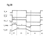
- Fig. 2B depicts a diagram of currents and voltages for an example of the slope generator 100 in operation.
- V_out V_I-Vbe_Q1(I_up) + Vbe_Q2(I_up)
- the voltage level generation unit 105 comprising the current switch 120 in combination with the current source 110 (providing the current I_q) only represent a preferred embodiment of the invention for providing the two voltage levels V_h and V_I to the current switch 40.
- the current switch 120 decouples the input and transforms the input signal(s) V_in to the voltage levels V_h and V_I. It is clear that though the input signal is depicted in Fig. 2A as differential input, any kind of input signal (differential or non-differential) can be applied.
- a pulse voltage source allowing to switch between the voltage levels V_h and V_I can also be applied.
- the offset voltage at the ramp node 25 is constantly at (V_h + V_I)/2.
- Fig. 3 depicts a second embodiment of a slope generator 200 according to the invention as a fully differential circuit.
- the differential generation of slopes makes the design less sensitive to common mode effects.
- the embodiment of Fig. 3 substantially corresponds to the embodiment of Fig. 2A. Components corresponding due to the differential characteristics are denoted with A and B.
- Figs. 2A and 3 The difference between the embodiments of Figs. 2A and 3 is that in Fig. 3 both the normal and the complementary input signals V_in are fed through separate slope-generators 100A and 100B built up substantially in accordance with the slope generator 100 of Fig. 2.
- the slope-generators 100A and 100B employ substantially identical capacitors C_rampA and C_rampB and substantially identical charge-/discharge currents.
- the voltage level generation unit 105 provides the differential voltage levels to the transistors Q1A and Q1B.
Landscapes
- Electronic Switches (AREA)
- Logic Circuits (AREA)
- Dc-Dc Converters (AREA)
- Analogue/Digital Conversion (AREA)
- Liquid Crystal Display Device Control (AREA)
Description
- The present invention relates to slope generators, according to the preamble to claim 1, for generating a slope between a first and a second voltage level.
- Slope generators (also referenced as waveform, ramp or sawtooth wave generators) are used in several applications for generating signals with a controllable slope. Typically, a current integrating capacitor is charged/discharged to produce a ramp signal.
- Fig. 1 depicts a
slope generator 10 as known in the art, e.g. a 1DB6 ("Snake") Slope Generator IC as used in the Hewlett-Packard HP8112A. Theslope generator 10 comprises a fixed connectedcurrent source 20 providing a charge current I_up to load a ramp-capacitor C_ramp from a voltage low level V_I to a voltage high level V_h as output voltage V_out at anode 25. Acurrent source 30 switchable by a current switch 40 (consisting of transistors Q1 and Q2) provides a current I_dn (whereby I_dn > I_up) to discharge the ramp-capacitor C_ramp from voltages V_h to V_I with a discharge current of I_dn - I_up. An input pulse V_in with fast edges at thecurrent switch 40 controls the coupling of thecurrent source 30 to the ramp-capacitor C_ramp. A low-level of the input pulse V_in switches on I_dn and a high level of the input pulse V_in switches off I_dn. - With the current I_dn being turned off, the ramp-capacitor C_ramp will be charged with a constant current I_up (thus generating a rising slope with the slew rate of dV/dt = I_up/C_ramp) until a clamping diode D2 (coupled to a clamping voltage V_cI_h) is taking over this current, thus stopping the charging. With I_dn being turned on, the ramp-capacitor C_ramp will be discharged with a constant current I_dn - I_up (thus generating a falling slope with the slew rate of dV/dt = -(I_dn - I_up)/C_ramp) until a clamping diode D1 (coupled to a clamping voltage V_cI_I) is taking over this current, thus stopping the discharging.
- The voltage levels V_I and V_h of the output voltage V_out at the
ramp node 25 of the ramp-capacitor C_ramp are derived from the clamping voltages V_cI_I and V_cI_h: - The clamping voltage V_cI_I and the forward voltage Vf_D1 at diode D1 are both dependent on the differences between the currents I_dn and I_up and on the temperature T. Accordingly, the clamping voltage V_cI_h and the forward voltage Vf_D2 at diode D2 are both dependent on the current I_up and the temperature T.
- The time to charge the capacitor C_ramp and thus the rising time T_rise of the
slope generator 10 is: - Accordingly and with I_dn > I_up, the time to discharge the capacitor C_ramp and thus the falling time T_fall of the
slope generator 10 is: - As apparent from equations (2) and (3), the timing of the
slope generator 10 directly depends on the voltage levels V_h and V_I. Therefore, significant effort has to be spent to compensate the thermal and current dependency of the clamping diodes D1 and D2. - Another, even more serious disadvantage of the
slope generator 10 of Fig. 1 is the capacitive loading by two clamping diodes (D1 and D2), thus limiting the minimum feasible ramp-capacitance C_ramp_eff, and accordingly, the minimum feasible transition times T_rise and T_fall. This is since the fastest slope (or transition time) is determined by the highest possible charging current and the lowest possible capacitance at thenode 25, whereby the capacitance at thenode 25 is determined by the capacitor C_ramp and parasitic capacitances. On the other hand, the parasitic capacitance of the clamping diodes D1 and D2 exhibits a strong dependency on the applied voltages, thus resulting in a negative impact on a desired linear slope. Since V_cI_I and V_cI_h represent low impedance nodes, the influence of parasitic capacitance of the clamping diodes D1 and D2 will add fully to the ramp capacitor C_ramp. - US-A-5,742,494 discloses an input-voltage-controlled pulse generator for driving a pulse converter or switch-mode power supply with a variable duty ratio and a fixed maximum test level and variable clock frequency.
- GB-A-1 430 397 discloses a sawtooth generator with the features of the preamble to claim 1.
- It is an object of the invention to provide an improved slope generator with a more accurate level clamping.
- The object is solved by
independent claim 1. Preferred embodiments are shown by the dependent claims. - A slope generator according to invention generates, in response to an input signal, a slope between a first and a second voltage level of an output voltage at an output node. The slope generator comprises a capacitor coupled to the output node, a first current source for providing a first constant current to the output node, and a second current source for providing a second constant current to the output node controlled by a first current switch. A control electrode of a first current path of the first current switch is coupled to and controlled by an input signal and a second current path is coupled to the output node. The first current switch provides the first and the second voltage levels, or corresponding voltage levels derived therefrom, to the output node.
- According to the invention, the first current switch represents a combined current switching/voltage level providing (clamping) circuit, thus diminishing the influence of parasitic capacitance loads at the ramp-node.
- In a preferred embodiment, the first current switch comprises two emitter-coupled transistors and a control electrode of the second current path is coupled to the output node. In contrast to the prior art as depicted in Fig. 1, wherein two diodes are connected to a low impedance node, this inventive embodiment provides just one diode connected to a low impedance node, thus allowing faster transition times for given ramp capacitor, charge currents and ramp voltage swings. Thus, the 'clamping principle' is to go - from the voltage levels V_I and V_h - one diode drop down and then one diode drop up again, thus directly transferring V_h and V_I to the ramp node. With matching diodes, all temperature and current dependencies are cancelled out with a very simple circuitry.
- The invention allows smaller achievable output transition times, a much simpler design and the good amplitude stability.
- Other objects and many of the attendant advantages of the present invention will be readily appreciated and become better understood by reference to the following detailed description when considering in connection with the accompanied drawings. Features that are or can be built up substantially equally or similarly are referred to with the same reference sign.
- Fig. 1
- depicts a
slope generator 10 as known in the art, - Fig. 2A
- depicts a first embodiment of a
slope generator 100 according to the invention, - Fig. 2B
- depicts a diagram of currents and voltages for an example of the
slope generator 100 of Fig. 2A in operation, and - Fig. 3
- depicts a second embodiment of a
slope generator 200 according to the invention as a differential circuit. - Fig. 2A depicts a first embodiment of a
slope generator 100 according to the invention. In accordance with theslope generator 10 of Fig. 1, theslope generator 100 comprises the ramp-capacitor C_ramp and the (positive)current source 20 providing the current I_up, both coupled to thenode 25. Theslope generator 100 further comprises the (negative)current source 30 providing the current I_dn to thecurrent switch 40 consisting of the transistors Q1 and Q2. Thecurrent switch 40 is coupled to and controlled by the input signal V_in. - In contrast to the
slope generator 10 of Fig. 1, a voltagelevel generation unit 105 provides the two voltage levels V_h and V_I to thecurrent switch 40. The voltagelevel generation unit 105 preferably comprises a current switch 120 (consisting of transistors Q3 and Q4) controlling the coupling of acurrent source 110 providing a current I_q. Thecurrent switch 120 generates the two voltage levels V_h and V_I at the collector (node Q4_C) of transistor Q4, following the input signal V_in. The collector of transistor Q4 is coupled to the base of transistor Q1 of thecurrent switch 40. Collector and base of transistor Q2 are commonly coupled tonode 25 thus rendering the transistor Q2 to be diode-connected. - Whereas the
current switch 40 in Fig. 1 only has the function of switching on or off the current I_dn tonode 25, thecurrent switch 40 in Fig. 2A further provides the two voltage levels V_h and V_I to thenode 25. - According to the invention (Fig. 2A) the
current source 30 is selected to provide a current I_dn = 2 x I_up for reasons which become clearer later. - In operation, the
slope generator 100 repetitively goes through four different states: - State #1: Low level state
- State #2: Transition from low level to high level
- State #3: High level state
- State #4: Transition back to low level
-
- Fig. 2B depicts a diagram of currents and voltages for an example of the
slope generator 100 in operation. - State #1: Assuming V_in is at a low level. Transistor Q3 will be turned off and transistor Q4 will be turned on. The collector of Q4 is coupled via an impedance Rc to a potential VCC, preferably ground level, thus generating the first voltage level:
node 25 is at an equilibrium point where no current is flowing into or out of the ramp capacitor C_ramp. The current I_up provided from thecurrent source 20 is forced to flow through the diode-connected transistor Q2. Since thecurrent source 30, coupled to the common emitters of transistors Q1 and Q2, pulls the current I_dn = 2 x I_up, exactly the same current I_up will flow through the transistor Q2 and the base-emitter diode of transistor Q1. - Having identical currents flowing through the base-emitter diodes of the transistors Q1 and Q2, the output voltage V_out at the ramp-
node 25 will be determined by the voltage level V_I and the base-emitter voltages Vbe_Q1 of transistor Q1 and Vbe_Q2 of transistor Q2: - Assuming a good matching of the transistors Q1 and Q2, the base-emitter voltages Vbe_Q1 and Vbe_Q2 will be substantially identical, thus keeping the output voltage V_out exactly at the voltage level V_I:
- State #2: Assuming a fast (relative to the intended slope at node 25) positive transition (from low level to high level) of the input signal V_in. Transistor Q3 will be turned on and transistor Q4 will be turned off, thus generating the second voltage level:
node 25 still is at V_I due to the capacitor C_ramp). Transistor Q1 will provide the full current I_dn, and no current will flow through transistor Q2. This forces thecurrent source 20 to provide the current I_up to the capacitor C_ramp, thus charging the capacitor C_ramp with a current I_ramp = I_up and at a rate of: - State #3: As the output voltage V_out is reaching the second voltage level V_h, transistor Q2 will start to turn on, taking over more and more of the current I_up from the
current source 20 until a new equilibrium is reached at theramp node 25. Now again, no current is flowing into or out of the ramp capacitor C_ramp. The current I_up from thecurrent source 20 has to flow through transistor Q2 and, since thecurrent source 30 pulls the current I_dn = 2 x I_up, the same current I_up will flow through transistor Q1. This, again, keeps the output voltage V_out at theramp node 25 exactly at the second voltage level V_h. - State #4: Assuming a fast (relative to the intended slope at node 25) negative transition (from high level to low level) of the input signal V_in. Transistor Q3 will be turned off and transistor Q4 will be turned on, thus generating again the first voltage level V_I = VCC- I_q x Rc at the collector of transistor Q4. Transistor Q1 will be turned off and transistor Q2 will be turned on (as the output voltage V_out at
node 25 still is at second voltage level V_h due to the capacitor C_ramp). The full current I_dn will be forced through transistor Q2. As I_dn is twice I_up, the effective discharging current through the capacitor C_ramp is-I_up. - Reentering State #1: As the output voltage V_out at
node 25 is reaching the first voltage level V_I, transistor Q1 will start to turn on, taking over a part of the current I_dn pulled by thecurrent source 30, until a new equilibrium is reached at theramp node 25. Now again, no current is flowing into or out of the ramp capacitor C_ramp. The current I_up is forced to flow through transistor Q2, and the same current I_up flows through transistor Q1 (see above), thus keeping the output voltage V_out exactly at the first voltage level V_I. - It is to be understood that the voltage
level generation unit 105 comprising thecurrent switch 120 in combination with the current source 110 (providing the current I_q) only represent a preferred embodiment of the invention for providing the two voltage levels V_h and V_I to thecurrent switch 40. Thecurrent switch 120, however, decouples the input and transforms the input signal(s) V_in to the voltage levels V_h and V_I. It is clear that though the input signal is depicted in Fig. 2A as differential input, any kind of input signal (differential or non-differential) can be applied. As an alternative to thecurrent switch 120, a pulse voltage source allowing to switch between the voltage levels V_h and V_I can also be applied. - For I_dn = 2 x I_up, the offset voltage at the
ramp node 25 is constantly at (V_h + V_I)/2. - Fig. 3 depicts a second embodiment of a
slope generator 200 according to the invention as a fully differential circuit. The differential generation of slopes makes the design less sensitive to common mode effects. The embodiment of Fig. 3 substantially corresponds to the embodiment of Fig. 2A. Components corresponding due to the differential characteristics are denoted with A and B. - The difference between the embodiments of Figs. 2A and 3 is that in Fig. 3 both the normal and the complementary input signals V_in are fed through separate slope-
generators 100A and 100B built up substantially in accordance with theslope generator 100 of Fig. 2. The slope-generators 100A and 100B employ substantially identical capacitors C_rampA and C_rampB and substantially identical charge-/discharge currents. The voltagelevel generation unit 105 provides the differential voltage levels to the transistors Q1A and Q1B. - With a positive step at V_in a positive slope is generated at
node 25A via the transistors Q1A and Q2A. At the same time, a negative slope with the substantially identical transition time is generated atnode 25B via transistors Q1B and Q2B, thus generating a differential output signal V_out.
Claims (6)
- A slope generator (100) comprising:a capacitor (C_ramp) coupled to the output node (25),an input node (Q4_C) for receiving an input signal (V_in) with a first (V_I) and a second (V_h) voltage level,an output node (25) for providing, in response to the input signal (V_in), a voltage slope between the first (V_I) and the second (V_h) voltage level as an output voltage (V_out),whereby:a first current source (20) for providing a first constant current (I_up) to the output node (25),a first current switch (40) having a first transistor (Q1) in a first current path and a second transistor (Q2) in a second current path, a control electrode of the first transistor (Q1) being coupled to and controlled by the input signal (V_in), a first current electrode of the first transistor (Q1 ) being coupled to a first current electrode of the second transistor (Q2) as common current electrodes, a second current electrode and a control electrode of the second transistor (Q2) being coupled diode-connected to the output node (25), anda second current source (30) for providing a second current (I_dn) to the common current electrodes of the first transistor (Q1) and the second transistor (Q2),the first current switch (40) provides the first (V_I) and the second (V_h) voltage levels of the input signal (V_in) to the output node (25),characterized in that the second current (I_dn) is a constant current and is twice the first current (I_up).
- The slope generator (100) of claim 1, wherein the first and the second transistors (Q1, Q2) are emitter-coupled.
- The slope generator (100) of claim 1 or 2, further comprising:
a voltage level generation unit (105; 120, 110) for providing the first (V_I) and the second (V_h) voltage levels, derived from the input signal (V_in), to the control electrode of the first current path of the current switch (40). - The slope generator (100) of claim 3, characterized in that the voltage level generation unit (105; 120, 110) comprises a second current switch (Q3, Q4) controlling a third current source (110).
- The slope generator (100) of any one of the above claims, characterized in that the capacitor (C_ramp) is charged by the first current source (20) for generating a first voltage slope (#2).
- The slope generator (100) of any one of the above claims, characterized in that the capacitor (C_ramp) is discharged by the second current source (30) for generating a second voltage slope (#4).
Priority Applications (4)
| Application Number | Priority Date | Filing Date | Title |
|---|---|---|---|
| EP98124629A EP0959561B1 (en) | 1998-12-23 | 1998-12-23 | Slope generator |
| DE69800694T DE69800694T2 (en) | 1998-12-23 | 1998-12-23 | Circuit for generating signals with adjustable slope |
| US09/453,771 US6316972B1 (en) | 1998-12-23 | 1999-12-02 | Slope generator |
| JP11364576A JP2000232341A (en) | 1998-12-23 | 1999-12-22 | Slope generator |
Applications Claiming Priority (1)
| Application Number | Priority Date | Filing Date | Title |
|---|---|---|---|
| EP98124629A EP0959561B1 (en) | 1998-12-23 | 1998-12-23 | Slope generator |
Publications (2)
| Publication Number | Publication Date |
|---|---|
| EP0959561A1 EP0959561A1 (en) | 1999-11-24 |
| EP0959561B1 true EP0959561B1 (en) | 2001-04-11 |
Family
ID=8233241
Family Applications (1)
| Application Number | Title | Priority Date | Filing Date |
|---|---|---|---|
| EP98124629A Expired - Lifetime EP0959561B1 (en) | 1998-12-23 | 1998-12-23 | Slope generator |
Country Status (4)
| Country | Link |
|---|---|
| US (1) | US6316972B1 (en) |
| EP (1) | EP0959561B1 (en) |
| JP (1) | JP2000232341A (en) |
| DE (1) | DE69800694T2 (en) |
Families Citing this family (3)
| Publication number | Priority date | Publication date | Assignee | Title |
|---|---|---|---|---|
| JP2001326562A (en) * | 2000-05-15 | 2001-11-22 | Nec Corp | Variable delay circuit |
| US6603335B1 (en) * | 2002-06-11 | 2003-08-05 | Sige Semiconductor Inc. | Ramp circuit to reduce spectral regrowth of power amplifiers |
| JP6294651B2 (en) * | 2013-12-11 | 2018-03-14 | 株式会社日立情報通信エンジニアリング | Reference waveform generation circuit, apparatus, and method |
Family Cites Families (9)
| Publication number | Priority date | Publication date | Assignee | Title |
|---|---|---|---|---|
| DE2262732C3 (en) * | 1972-12-21 | 1978-08-24 | Deutsche Itt Industries Gmbh, 7800 Freiburg | Monolithically integrable sawtooth generator |
| DE2737432C3 (en) * | 1977-08-19 | 1980-03-06 | Hewlett-Packard Gmbh, 7030 Boeblingen | Integrator circuit with limitation |
| US5006739A (en) * | 1987-06-15 | 1991-04-09 | Hitachi, Ltd. | Capacitive load drive circuit |
| US5087827A (en) * | 1991-02-11 | 1992-02-11 | Tektronix, Inc. | Variable voltage transition circuit |
| JP2840490B2 (en) * | 1991-11-29 | 1998-12-24 | 三菱電機株式会社 | Active filter circuit |
| DE4438671C1 (en) * | 1994-10-28 | 1996-05-15 | Sgs Thomson Microelectronics | Circuit arrangement for controlling a converter |
| US5874837A (en) * | 1997-04-28 | 1999-02-23 | Pericom Semiconductor Corp. | CMOS PECL driver with programmable current for varying voltage swings and termination types |
| US6028459A (en) * | 1998-04-20 | 2000-02-22 | National Semiconductor Corporation | Track and hold circuit with clamp |
| US6121805A (en) * | 1998-10-08 | 2000-09-19 | Exar Corporation | Universal duty cycle adjustment circuit |
-
1998
- 1998-12-23 DE DE69800694T patent/DE69800694T2/en not_active Expired - Fee Related
- 1998-12-23 EP EP98124629A patent/EP0959561B1/en not_active Expired - Lifetime
-
1999
- 1999-12-02 US US09/453,771 patent/US6316972B1/en not_active Expired - Fee Related
- 1999-12-22 JP JP11364576A patent/JP2000232341A/en active Pending
Also Published As
| Publication number | Publication date |
|---|---|
| DE69800694D1 (en) | 2001-05-17 |
| DE69800694T2 (en) | 2001-09-13 |
| US6316972B1 (en) | 2001-11-13 |
| JP2000232341A (en) | 2000-08-22 |
| EP0959561A1 (en) | 1999-11-24 |
Similar Documents
| Publication | Publication Date | Title |
|---|---|---|
| US5329210A (en) | High-speed driver for an LED communication system or the like | |
| US9059688B2 (en) | High-precision oscillator systems with feed forward compensation for CCFL driver systems and methods thereof | |
| EP0856935B1 (en) | Charge pump circuit | |
| US5227672A (en) | Digital clock selection and changeover apparatus | |
| JP2004104645A (en) | Triangular wave generating device, pulse width modulation signal generating device and external synchronization/internal synchronization/asynchronization switching device | |
| US6891443B2 (en) | Oscillator | |
| EP0959561A1 (en) | Slope generator | |
| US5146188A (en) | Constant current circuit and an oscillating circuit controlled by the same | |
| US4847520A (en) | Fast PNP transistor turn-off circuit | |
| EP0745921B1 (en) | Transistor current generator stage for integrated analog circuits | |
| JPH01268454A (en) | Gradual starter for switching source | |
| US6194936B1 (en) | Pulse generator provided with a duty-factor limiting function | |
| US4554464A (en) | Propagation delay generator | |
| EP0449208B1 (en) | Level converter for converting ECL-level signal voltage to TTL-level signal voltage | |
| US4600897A (en) | Voltage-controlled oscillator of emitter-coupled astable multivibrator type | |
| KR19990076264A (en) | Charge-Discharge Oscillator Using Constant Current and Its Oscillation Method | |
| KR940010481A (en) | Low frequency oscillator | |
| US5367203A (en) | System for determining the time at which an analog voltage crosses a voltage threshold | |
| US4504928A (en) | Current ramp generator | |
| US5289052A (en) | Monostable multivibrator | |
| KR100228284B1 (en) | Discharge circuit using timing sequence | |
| EP0465167A2 (en) | Non-threshold logic circuit | |
| US4916332A (en) | Timing and supply bias circuit using one capacitor | |
| KR890004648B1 (en) | Voltage control oscillator | |
| JPH01289311A (en) | Saw-tooth wave oscillator stage |
Legal Events
| Date | Code | Title | Description |
|---|---|---|---|
| PUAI | Public reference made under article 153(3) epc to a published international application that has entered the european phase |
Free format text: ORIGINAL CODE: 0009012 |
|
| 17P | Request for examination filed |
Effective date: 19990911 |
|
| AK | Designated contracting states |
Kind code of ref document: A1 Designated state(s): DE FR GB |
|
| AX | Request for extension of the european patent |
Free format text: AL;LT;LV;MK;RO;SI |
|
| 17Q | First examination report despatched |
Effective date: 20000204 |
|
| AKX | Designation fees paid |
Free format text: DE FR GB |
|
| GRAG | Despatch of communication of intention to grant |
Free format text: ORIGINAL CODE: EPIDOS AGRA |
|
| GRAG | Despatch of communication of intention to grant |
Free format text: ORIGINAL CODE: EPIDOS AGRA |
|
| GRAH | Despatch of communication of intention to grant a patent |
Free format text: ORIGINAL CODE: EPIDOS IGRA |
|
| GRAH | Despatch of communication of intention to grant a patent |
Free format text: ORIGINAL CODE: EPIDOS IGRA |
|
| GRAA | (expected) grant |
Free format text: ORIGINAL CODE: 0009210 |
|
| RAP1 | Party data changed (applicant data changed or rights of an application transferred) |
Owner name: AGILENT TECHNOLOGIES, INC. |
|
| AK | Designated contracting states |
Kind code of ref document: B1 Designated state(s): DE FR GB |
|
| REF | Corresponds to: |
Ref document number: 69800694 Country of ref document: DE Date of ref document: 20010517 |
|
| ET | Fr: translation filed | ||
| RAP2 | Party data changed (patent owner data changed or rights of a patent transferred) |
Owner name: AGILENT TECHNOLOGIES INC. |
|
| RAP2 | Party data changed (patent owner data changed or rights of a patent transferred) |
Owner name: AGILENT TECHNOLOGIES INC. A DELAWARE CORPORATION |
|
| RAP2 | Party data changed (patent owner data changed or rights of a patent transferred) |
Owner name: AGILENT TECHNOLOGIES, INC. (A DELAWARE CORPORATION |
|
| PGFP | Annual fee paid to national office [announced via postgrant information from national office to epo] |
Ref country code: FR Payment date: 20011130 Year of fee payment: 4 |
|
| REG | Reference to a national code |
Ref country code: GB Ref legal event code: IF02 |
|
| PLBE | No opposition filed within time limit |
Free format text: ORIGINAL CODE: 0009261 |
|
| STAA | Information on the status of an ep patent application or granted ep patent |
Free format text: STATUS: NO OPPOSITION FILED WITHIN TIME LIMIT |
|
| 26N | No opposition filed | ||
| PG25 | Lapsed in a contracting state [announced via postgrant information from national office to epo] |
Ref country code: FR Free format text: LAPSE BECAUSE OF NON-PAYMENT OF DUE FEES Effective date: 20030901 |
|
| REG | Reference to a national code |
Ref country code: FR Ref legal event code: ST |
|
| PGFP | Annual fee paid to national office [announced via postgrant information from national office to epo] |
Ref country code: GB Payment date: 20051214 Year of fee payment: 8 |
|
| PGFP | Annual fee paid to national office [announced via postgrant information from national office to epo] |
Ref country code: DE Payment date: 20070131 Year of fee payment: 9 |
|
| GBPC | Gb: european patent ceased through non-payment of renewal fee |
Effective date: 20061223 |
|
| PG25 | Lapsed in a contracting state [announced via postgrant information from national office to epo] |
Ref country code: GB Free format text: LAPSE BECAUSE OF NON-PAYMENT OF DUE FEES Effective date: 20061223 |
|
| PG25 | Lapsed in a contracting state [announced via postgrant information from national office to epo] |
Ref country code: DE Free format text: LAPSE BECAUSE OF NON-PAYMENT OF DUE FEES Effective date: 20080701 |