EP0959559A1 - Direct broadcast satellite tuner - Google Patents
Direct broadcast satellite tuner Download PDFInfo
- Publication number
- EP0959559A1 EP0959559A1 EP99303816A EP99303816A EP0959559A1 EP 0959559 A1 EP0959559 A1 EP 0959559A1 EP 99303816 A EP99303816 A EP 99303816A EP 99303816 A EP99303816 A EP 99303816A EP 0959559 A1 EP0959559 A1 EP 0959559A1
- Authority
- EP
- European Patent Office
- Prior art keywords
- signal
- circuit
- converter
- demodulator
- intermediate frequency
- Prior art date
- Legal status (The legal status is an assumption and is not a legal conclusion. Google has not performed a legal analysis and makes no representation as to the accuracy of the status listed.)
- Granted
Links
Images

Classifications
-
- H—ELECTRICITY
- H03—ELECTRONIC CIRCUITRY
- H03D—DEMODULATION OR TRANSFERENCE OF MODULATION FROM ONE CARRIER TO ANOTHER
- H03D7/00—Transference of modulation from one carrier to another, e.g. frequency-changing
- H03D7/16—Multiple-frequency-changing
- H03D7/165—Multiple-frequency-changing at least two frequency changers being located in different paths, e.g. in two paths with carriers in quadrature
Definitions
- the present invention relates to a DBS (direct broadcast by satellite) tuner for receiving analog and digital satellite broadcast.
- DBS direct broadcast by satellite
- reception of both analog-signal-based and digital-signal-based satellite broadcast is achieved, for satellite broadcast carried by an FM (frequency-modulated) analog signal, by receiving it by the use of an analog-signal receiver, and, for satellite broadcast carried by a QPSK-modulated digital signal, by receiving it by the use of a digital-signal receiver; that is, it is necessary to use two set-top boxes in total, or alternatively a TV (television) receiver incorporating two tuners corresponding thereto.
- FM frequency-modulated
- QPSK-modulated digital signal by receiving it by the use of a digital-signal receiver
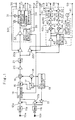
- Fig. 3 is a block diagram of a conventional DBS (direct broadcast by satellite) tuner for receiving satellite broadcast by receiving a QPSK-modulated digital signal and an FM (frequency-modulated) analog signal.
- two RF signals are fed in to the tuner via input terminals 10a and 10b, respectively, and are then delivered individually to RF circuits each consisting of a high-pass filter 11a or 11b and an RF amplifier circuit 12a or 12b.
- One of these two RF amplifier circuits 12a and 12b is selected for activation at a time by a switching circuit 13 composed of transistors.
- One of the two RF signals fed in to the tuner via the input terminals 10a and 10b is selected by the above-mentioned switching circuit 13, is then amplified by the RF amplifier circuit 12a or 12b, and is then subjected to level adjustment by an attenuator 14 that is common to the two signals.
- the RF signal is subjected to pass band adjustment by an RF band-pass filter 15, is then mixed by a mixer 16 with a local oscillation signal fed from a local oscillation circuit 18 controlled by a PLL synthesizer circuit 19 and an LPF (low-pass filter) 17, and is thereby converted into an IF (intermediate-frequency) signal having a frequency of, for example, 479.5 MHz.
- the IF signal thus obtained by frequency conversion is then amplified by an IF amplifier circuit 20, is then passed through an IF band-pass filter 21, is then further amplified by an IF amplifier circuit 22, and is then divided into two signals.
- One of the signals thus obtained by division is fed to an FM demodulator 301, where the signal is subjected to FM demodulation to produce an FM detected signal.
- the other of the signals obtained by division after amplification by the IF amplifier circuit 22 is fed to an I/Q converter 401, where the signal is subjected to frequency conversion so as to be converted into a base band signal to produce two signals, called the I and Q signals, having a phase difference of 90 degrees with respect to each other.
- the front-end portion of the tuner including the RF amplifier circuit 12a, the RF attenuator 14, the RF band-pass filter 15, the mixer 16, the first local oscillation circuit 18, the PLL synthesizer circuit 19, and the IF amplifier circuit 20, and the IF amplifier portion including the band-pass filter 21 are common to analog and digital signals, and thus their basic circuit design can be shared between analog and digital signals.
- the I/Q converter 401 used to achieve QPSK demodulation of the digital signal and the FM demodulator 301 used to achieve FM demodulation of the analog signal are required separately.
- the I/Q converter 401 uses an oscillation circuit 41 having a resonator (for example, a SAW resonator) that resonates at 479.5 MHz (or 402.78 MHz), and the FM demodulator 301 uses a VCO (voltage-controlled oscillator) 31 that oscillates near (i.e. not exactly at) 479.5 MHz (or 402.78 MHz) (the FM demodulator minimizes the noise occurring when the C/N ratio is low by shifting the oscillation frequency of the VCO). If these two oscillation circuits are placed close to each other within the same chassis, their oscillation frequencies, very close to each other, tend to cause spurious oscillation and pulling of the oscillation frequency.
- a resonator for example, a SAW resonator
- VCO voltage-controlled oscillator
- the VCO 41 of the I/Q converter 401 provided for the processing of a digitally modulated signal, is affected by the VCO 31 of the FM demodulator 301, the phase noise in the I/Q converter increases, and thus the overall phase noise throughout the tuner increases, degrading the bit error rate after QPSK demodulation in the QPSK demodulation circuit (not shown) placed in the stage succeeding to the DBS tuner.
- the FM demodulator 301 and the I/Q converter 401 only one is selected for activation at a time, and the other is brought into an inactive state.
- the signal type i.e. when the tuner is switched from the state for receiving an FM signal to the state for receiving a QPSK signal
- there occurs a time period (a short time period) in which both become active momentarily, and the above problem occurs during this time period.
- An object of the present invention is to miniaturize a tuner for receiving satellite broadcast having an FM modulator and an I/Q converter arranged within a single chassis and to reduce the mutual interference between the FM modulator and the I/Q converter in such a tuner.
- a DBS tuner that receives satellite broadcast by receiving a QPSK modulated digital signal and an FM (frequency modulated) analog signal
- the tuner sharing a highfrequency signal processing circuit provided in a front-end portion for receiving an RF (radio frequency) signal having a frequency around 1 to 2 GHz and an intermediate frequency amplifier portion including an intermediate frequency amplifier circuit for amplifying a signal obtained by converting a received signal to an intermediate frequency and a band-pass filter
- the tuner having an I/Q converter for processing a modulated digital signal output from the band-pass filter and an FM demodulator for processing an FM analog signal output from the band-pass filter
- amplifier circuits are provided between the output side of the band-pass filter and the input side of the FM demodulator and between the output side of the band-pass filter and the input side of the I/Q converter.
- amplifier circuits are provided in the stage following the output of the band-pass filter both on the input side of the FM demodulator and on the input side of the I/Q converter. This helps improve the isolation between the signal paths to the FM demodulator and to the I/Q converter and thereby reduce the interference between the oscillation circuits of the FM demodulator and the I/Q converter. In this way, it is possible to reduce the effect of the signal returning along the signal path from the I/Q converter to the FM demodulator and of the signal returning along the signal path from the FM demodulator to the I/Q converter. In particular, this is effective in reducing the phase noise occurring in the VCO of the I/Q converter.
- the intermediate frequency amplifier circuit is placed between the FM demodulator and the I/Q converter. This makes it possible to reduce the spatial interference between the oscillation circuits of the FM demodulator and the I/Q converter by the use of a chassis of a relatively small volume.
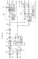
- Fig. 1 is a block diagram showing the circuit configuration of a DBS tuner for receiving satellite broadcast according to the invention.
- Fig. 1 such components as are found also in the conventional example shown in Fig. 3 are identified with the same reference numerals and symbols.
- Fig. 1 two RF signals are fed in to the tuner via input terminals 10a and 10b, respectively, and are then delivered individually to RF circuits each consisting of a high-pass filter 11a or 11b and an RF amplifier circuit 12a or 12b.
- RF circuits each consisting of a high-pass filter 11a or 11b and an RF amplifier circuit 12a or 12b.
- One of these two RF amplifier circuits 12a and 12b is selected for activation at a time by a switching circuit 13 composed of transistors.
- the two RF signals fed in to the tuner via the input terminals 10a and 10b are amplified by one of the RF amplifier circuits 12a and 12b as selected by the above-mentioned switching circuit 13, and is then subjected to level adjustment by an attenuator 14 that is common to the two signals.
- the RF signal is passed through an RF band-pass filter 15, is then mixed by a mixer 16 with a local oscillation signal fed from a local oscillation circuit 18 controlled by a PLL synthesizer circuit 19 and an LPF (low-pass filter) 17, and is thereby converted into an IF (intermediate-frequency) signal having a frequency of, for example, 479.5 MHz.
- the IF signal thus obtained by frequency conversion is then amplified by an IF amplifier circuit 20, is then passed through an IF band-pass filter 21, and is then divided into two signals, which are fed to IF amplifier circuits 22a and 22b.
- the IF signal amplified by the IF amplifier circuit 22a is subjected to FM demodulation by an FM demodulator 301 to produce an FM detected signal.
- the IF signal amplified by the IF amplifier circuit 22b is subjected to frequency conversion by an I/Q converter 401 so as to be converted into a base band signal to produce two signals, called the I and Q signals, having a phase difference of 90 degrees with respect to each other.
- the output obtained from the band-pass filter 21 of the IF amplifier portion is divided into two signals that are amplified individually by the IF amplifier circuits 22a and 22b.
- This helps improve the isolation between the input to the FM demodulator 301 and the input to the I/Q converter 401 and thereby reduce the mutual effect between the I/Q converter 401 and the FM demodulator 301 caused by signals returning from the former to the latter and vice versa. In particular, this is effective in reducing the phase noise occurring in the VCO of the I/Q converter 401.
- the FM demodulator 301 and the I/Q converter 401 are each formed as an integrated circuit.
- Fig. 2 is a diagram showing the arrangement of the individual circuit blocks within the chassis of the tuner according to the invention.
- reference numeral 1 represents a section for housing the circuit block of the RF amplifiers 12a and 12b;
- reference numeral 2 represents a section for housing the frequency conversion circuit block including the RF attenuator 14, the RF band-pass filter 15, and the mixer circuit 16;
- reference numeral 3 represents a section for housing the local oscillator circuit block including the local oscillator circuit 18 and the synthesizer circuit;
- reference numeral 4 represents a section for housing the circuit block of the FM demodulator 301;
- reference numeral 5 represents a section for housing the IF amplifier circuit block including the IF amplifier circuit 20 and the band-pass filter 21;
- reference numeral 6 represents a section for housing the circuit block of the I/Q converter circuit 401; and
- reference symbols a and b represent the first and second input terminals, respectively, of the DBS tuner for receiving satellite broadcast.
- circuit blocks 1 to 6 are formed within a metal chassis, and are shielded from one another by metal shields 8A to 8E. Moreover, as shown in Fig. 2, between the section 4 for housing the circuit block of the FM demodulator 301 and the section 6 for housing the circuit block of the I/Q converter circuit 401 is arranged the section 5 for housing the IF amplifier circuit block including the IF amplifier 20 and the band-pass filter 21 so that the section 4 for housing the circuit block of the FM demodulator 301 and the section 6 for housing the circuit block of the I/Q converter circuit 401 are isolated from each other with the section 5 for housing the IF amplifier circuit block arranged between them.
- the FM demodulator 301 is provided with an amplifier circuit 32, a PLL-type FM demodulator circuit 33, a window comparator 39, and an AGC detection circuit 35.
- Reference numeral 36 represents a terminal at which the FM demodulator 301 receives electric power.
- Reference numeral 37 represents an output terminal at which the FM demodulator 301 outputs the FM demodulated signal.
- Reference numerals 38 and 39 represent terminals at which the output of a widow comparator 34 is output as a first AFT (automatic fine tuning) signal and a second AFT signal.
- the AGC signal output from the AGC detection circuit 35 is fed to the RF attenuator 14 and also to an analog AGC terminal 30.
- the I/Q converter 401 is provided with an amplifier 42, demodulators 43 and 44, amplifiers 45 to 48, low-pass filters 49 and 50, AGC amplifiers 51 and 52, a 90-degree phase shifter 53, and an AGC detection circuit 54.
- Reference numeral 55 represents a supplied power terminal at which the I/Q converter 401 receives electric power.
- Reference numeral 56 represents an AGC signal input terminal
- reference numeral 57 represents an I signal output terminal
- reference numeral 58 represents a Q signal output terminal.
- the output of the AGC detection circuit 54 is fed to the attenuator 14 and also to a terminal 59.
- the above-mentioned terminals 30, 37, 38, and 39 are connected to a circuit (not shown) that processes the FM demodulated signal.
- the above-mentioned terminals 57, 58, and 59 are connected to a circuit (not shown) that processes the I and Q signals.
Abstract
Description
Claims (3)
- A DBS tuner having an RF circuit for processing an RF signal, an intermediate frequency amplifier portion including an intermediate frequency amplifier circuit for amplifying a signal obtained by converting the RF signal to an intermediate frequency and a band-pass filter, an I/Q converter for processing a modulated digital signal output from the band-pass filter, and an FM demodulator for processing an FM modulated analog signal output from the band-pass filter,
wherein a first intermediate frequency signal amplifier circuit is provided between an output side of the band-pass filter and an input side of the FM demodulator and a second intermediate frequency signal amplifier circuit is provided between the output side of the band-pass filter and an input side of the I/Q converter. - A DBS tuner as claimed in claim 1,
wherein the intermediate frequency amplifier portion, the FM demodulator, and the I/Q converter are arranged in separate sections secured inside a chassis of the tuner and partitioned by shielding members. - A DBS tuner as claimed in claim 2,
wherein the I/Q converter is arranged between the intermediate frequency amplifier portion and the FM demodulator.
Applications Claiming Priority (2)
| Application Number | Priority Date | Filing Date | Title |
|---|---|---|---|
| JP14104498 | 1998-05-22 | ||
| JP14104498A JP3471219B2 (en) | 1998-05-22 | 1998-05-22 | DBS tuner for satellite broadcast reception |
Publications (2)
| Publication Number | Publication Date |
|---|---|
| EP0959559A1 true EP0959559A1 (en) | 1999-11-24 |
| EP0959559B1 EP0959559B1 (en) | 2004-07-14 |
Family
ID=15282953
Family Applications (1)
| Application Number | Title | Priority Date | Filing Date |
|---|---|---|---|
| EP19990303816 Expired - Lifetime EP0959559B1 (en) | 1998-05-22 | 1999-05-17 | Direct broadcast satellite tuner |
Country Status (4)
| Country | Link |
|---|---|
| EP (1) | EP0959559B1 (en) |
| JP (1) | JP3471219B2 (en) |
| CN (1) | CN1118188C (en) |
| DE (1) | DE69918606T2 (en) |
Cited By (2)
| Publication number | Priority date | Publication date | Assignee | Title |
|---|---|---|---|---|
| EP1592140A3 (en) * | 2004-04-27 | 2006-09-06 | Robert Bosch Gmbh | Device for the reception of broadcast signals |
| US7212474B2 (en) | 2002-08-19 | 2007-05-01 | Koninklijke Philips Electronics N.V. | Detecting anomalies in a scanning signal |
Families Citing this family (6)
| Publication number | Priority date | Publication date | Assignee | Title |
|---|---|---|---|---|
| JP3741648B2 (en) | 2002-01-04 | 2006-02-01 | シャープ株式会社 | Digital / Analog tuner |
| JP4368592B2 (en) * | 2003-02-19 | 2009-11-18 | シャープ株式会社 | Digital broadcast receiving tuner and receiving apparatus having the same |
| JP2005136790A (en) * | 2003-10-31 | 2005-05-26 | Sanyo Electric Co Ltd | Analog/digital common front end module |
| KR100692596B1 (en) | 2004-05-06 | 2007-03-13 | 삼성전자주식회사 | Digital broadcasting transmission/reception capable of improving receiving performance and signal processing method thereof |
| JP2009147415A (en) | 2007-12-11 | 2009-07-02 | Sharp Corp | Receiving apparatus, and board installing member |
| JP2010278732A (en) * | 2009-05-28 | 2010-12-09 | Alps Electric Co Ltd | Intermediate frequency circuit for television broadcast receiving tuner |
Citations (2)
| Publication number | Priority date | Publication date | Assignee | Title |
|---|---|---|---|---|
| EP0766418A2 (en) * | 1995-09-26 | 1997-04-02 | SHARP Corporation | Digital satellite broadcasting receiver |
| EP0777335A2 (en) * | 1995-12-04 | 1997-06-04 | Sharp Kabushiki Kaisha | Satellite broadcast tuner capable of processing both QPSK modulation signal and FM signal |
-
1998
- 1998-05-22 JP JP14104498A patent/JP3471219B2/en not_active Expired - Fee Related
-
1999
- 1999-05-17 DE DE1999618606 patent/DE69918606T2/en not_active Expired - Fee Related
- 1999-05-17 EP EP19990303816 patent/EP0959559B1/en not_active Expired - Lifetime
- 1999-05-20 CN CN 99106782 patent/CN1118188C/en not_active Expired - Fee Related
Patent Citations (2)
| Publication number | Priority date | Publication date | Assignee | Title |
|---|---|---|---|---|
| EP0766418A2 (en) * | 1995-09-26 | 1997-04-02 | SHARP Corporation | Digital satellite broadcasting receiver |
| EP0777335A2 (en) * | 1995-12-04 | 1997-06-04 | Sharp Kabushiki Kaisha | Satellite broadcast tuner capable of processing both QPSK modulation signal and FM signal |
Cited By (2)
| Publication number | Priority date | Publication date | Assignee | Title |
|---|---|---|---|---|
| US7212474B2 (en) | 2002-08-19 | 2007-05-01 | Koninklijke Philips Electronics N.V. | Detecting anomalies in a scanning signal |
| EP1592140A3 (en) * | 2004-04-27 | 2006-09-06 | Robert Bosch Gmbh | Device for the reception of broadcast signals |
Also Published As
| Publication number | Publication date |
|---|---|
| DE69918606T2 (en) | 2005-08-25 |
| JP3471219B2 (en) | 2003-12-02 |
| JPH11341375A (en) | 1999-12-10 |
| CN1118188C (en) | 2003-08-13 |
| EP0959559B1 (en) | 2004-07-14 |
| DE69918606D1 (en) | 2004-08-19 |
| CN1237063A (en) | 1999-12-01 |
Similar Documents
| Publication | Publication Date | Title |
|---|---|---|
| US5950112A (en) | Satelite broadcast tuner capable of processing both QPSK modulation signal and FM signal | |
| JP3444727B2 (en) | Digital satellite broadcasting receiver | |
| US7831198B2 (en) | Broadcast receiving apparatus | |
| JPH0964770A (en) | Tuner integrally receiving ground broadcasting and satellite broadcasting | |
| JPS5957534A (en) | Indoor unit of receiver for satellite broadcast | |
| US8315584B2 (en) | Semiconductor integrated circuit and broadcast receiver | |
| EP0959559B1 (en) | Direct broadcast satellite tuner | |
| US6934523B2 (en) | Tuner | |
| US20070015479A1 (en) | Integrated wireless receiver and a wireless receiving method thereof | |
| JP2007116429A (en) | Broadcast receiving apparatus | |
| JPH07231273A (en) | Tuner for receiving satellite broadcast | |
| US5630214A (en) | Wide-band receiving apparatus with local oscillating circuit | |
| JP3128371B2 (en) | Receiver | |
| JP3502263B2 (en) | Tuner for digital broadcasting reception | |
| JP2006148533A (en) | Sound intermediate frequency conversion circuit | |
| US7145610B2 (en) | Receiving method and apparatus of analog television signals technical field | |
| KR101331663B1 (en) | Analog and digital satellite wave tuner | |
| JP3504847B2 (en) | DBS tuner for satellite broadcasting reception | |
| JPH08289221A (en) | Digital and analog sharing tuner | |
| JP3617513B2 (en) | Receiver | |
| JP3617521B2 (en) | Receiver | |
| JP3756037B2 (en) | Television tuner | |
| JP3714851B2 (en) | Television tuner | |
| JP2001119634A (en) | Satellite broadcast receiver | |
| JP4300170B2 (en) | Receiver |
Legal Events
| Date | Code | Title | Description |
|---|---|---|---|
| PUAI | Public reference made under article 153(3) epc to a published international application that has entered the european phase |
Free format text: ORIGINAL CODE: 0009012 |
|
| AK | Designated contracting states |
Kind code of ref document: A1 Designated state(s): DE FR GB NL |
|
| AX | Request for extension of the european patent |
Free format text: AL;LT;LV;MK;RO;SI |
|
| 17P | Request for examination filed |
Effective date: 20000121 |
|
| AKX | Designation fees paid |
Free format text: DE FR GB NL |
|
| GRAP | Despatch of communication of intention to grant a patent |
Free format text: ORIGINAL CODE: EPIDOSNIGR1 |
|
| GRAS | Grant fee paid |
Free format text: ORIGINAL CODE: EPIDOSNIGR3 |
|
| GRAA | (expected) grant |
Free format text: ORIGINAL CODE: 0009210 |
|
| AK | Designated contracting states |
Kind code of ref document: B1 Designated state(s): DE FR GB NL |
|
| REG | Reference to a national code |
Ref country code: GB Ref legal event code: FG4D |
|
| REF | Corresponds to: |
Ref document number: 69918606 Country of ref document: DE Date of ref document: 20040819 Kind code of ref document: P |
|
| ET | Fr: translation filed | ||
| PLBE | No opposition filed within time limit |
Free format text: ORIGINAL CODE: 0009261 |
|
| STAA | Information on the status of an ep patent application or granted ep patent |
Free format text: STATUS: NO OPPOSITION FILED WITHIN TIME LIMIT |
|
| 26N | No opposition filed |
Effective date: 20050415 |
|
| PGFP | Annual fee paid to national office [announced via postgrant information from national office to epo] |
Ref country code: DE Payment date: 20080522 Year of fee payment: 10 |
|
| PGFP | Annual fee paid to national office [announced via postgrant information from national office to epo] |
Ref country code: NL Payment date: 20080501 Year of fee payment: 10 |
|
| PGFP | Annual fee paid to national office [announced via postgrant information from national office to epo] |
Ref country code: GB Payment date: 20080521 Year of fee payment: 10 |
|
| GBPC | Gb: european patent ceased through non-payment of renewal fee |
Effective date: 20090517 |
|
| NLV4 | Nl: lapsed or anulled due to non-payment of the annual fee |
Effective date: 20091201 |
|
| PG25 | Lapsed in a contracting state [announced via postgrant information from national office to epo] |
Ref country code: NL Free format text: LAPSE BECAUSE OF NON-PAYMENT OF DUE FEES Effective date: 20091201 |
|
| REG | Reference to a national code |
Ref country code: FR Ref legal event code: ST Effective date: 20100129 |
|
| PG25 | Lapsed in a contracting state [announced via postgrant information from national office to epo] |
Ref country code: FR Free format text: LAPSE BECAUSE OF NON-PAYMENT OF DUE FEES Effective date: 20090602 |
|
| PGFP | Annual fee paid to national office [announced via postgrant information from national office to epo] |
Ref country code: FR Payment date: 20080514 Year of fee payment: 10 |
|
| PG25 | Lapsed in a contracting state [announced via postgrant information from national office to epo] |
Ref country code: GB Free format text: LAPSE BECAUSE OF NON-PAYMENT OF DUE FEES Effective date: 20090517 |
|
| PG25 | Lapsed in a contracting state [announced via postgrant information from national office to epo] |
Ref country code: DE Free format text: LAPSE BECAUSE OF NON-PAYMENT OF DUE FEES Effective date: 20091201 |