EP0956629B1 - An a.c. current distribution system - Google Patents
An a.c. current distribution system Download PDFInfo
- Publication number
- EP0956629B1 EP0956629B1 EP98905118A EP98905118A EP0956629B1 EP 0956629 B1 EP0956629 B1 EP 0956629B1 EP 98905118 A EP98905118 A EP 98905118A EP 98905118 A EP98905118 A EP 98905118A EP 0956629 B1 EP0956629 B1 EP 0956629B1
- Authority
- EP
- European Patent Office
- Prior art keywords
- load
- conductive means
- series
- tracks
- distribution system
- Prior art date
- Legal status (The legal status is an assumption and is not a legal conclusion. Google has not performed a legal analysis and makes no representation as to the accuracy of the status listed.)
- Expired - Lifetime
Links
- 238000004804 winding Methods 0.000 claims description 36
- 230000005684 electric field Effects 0.000 claims description 12
- 230000008878 coupling Effects 0.000 claims description 10
- 238000010168 coupling process Methods 0.000 claims description 10
- 238000005859 coupling reaction Methods 0.000 claims description 10
- 238000000034 method Methods 0.000 claims description 4
- -1 polypropylene Polymers 0.000 claims description 4
- RYGMFSIKBFXOCR-UHFFFAOYSA-N Copper Chemical compound [Cu] RYGMFSIKBFXOCR-UHFFFAOYSA-N 0.000 claims description 2
- 229920000265 Polyparaphenylene Polymers 0.000 claims description 2
- 239000004743 Polypropylene Substances 0.000 claims description 2
- UCKMPCXJQFINFW-UHFFFAOYSA-N Sulphide Chemical compound [S-2] UCKMPCXJQFINFW-UHFFFAOYSA-N 0.000 claims description 2
- 229910052802 copper Inorganic materials 0.000 claims description 2
- 239000010949 copper Substances 0.000 claims description 2
- 239000004033 plastic Substances 0.000 claims description 2
- 229920003023 plastic Polymers 0.000 claims description 2
- 229920000728 polyester Polymers 0.000 claims description 2
- 229920001155 polypropylene Polymers 0.000 claims description 2
- 239000011810 insulating material Substances 0.000 claims 2
- 239000000463 material Substances 0.000 claims 1
- 230000010363 phase shift Effects 0.000 description 2
- 230000001105 regulatory effect Effects 0.000 description 2
- 238000002955 isolation Methods 0.000 description 1
- 229920006395 saturated elastomer Polymers 0.000 description 1
Images


Classifications
-
- H—ELECTRICITY
- H01—ELECTRIC ELEMENTS
- H01F—MAGNETS; INDUCTANCES; TRANSFORMERS; SELECTION OF MATERIALS FOR THEIR MAGNETIC PROPERTIES
- H01F29/00—Variable transformers or inductances not covered by group H01F21/00
- H01F29/14—Variable transformers or inductances not covered by group H01F21/00 with variable magnetic bias
-
- H—ELECTRICITY
- H01—ELECTRIC ELEMENTS
- H01F—MAGNETS; INDUCTANCES; TRANSFORMERS; SELECTION OF MATERIALS FOR THEIR MAGNETIC PROPERTIES
- H01F29/00—Variable transformers or inductances not covered by group H01F21/00
- H01F29/14—Variable transformers or inductances not covered by group H01F21/00 with variable magnetic bias
- H01F2029/143—Variable transformers or inductances not covered by group H01F21/00 with variable magnetic bias with control winding for generating magnetic bias
Definitions
- THIS INVENTION relates to improvements in or relating to an a.c. current distribution system and more particularly relates to an a.c. current distribution system for minimising the electric field along the current distribution system.
- the two voltages are fed down a power bus comprising a pair of conductive tracks which run parallel to one another and are separated from one another.
- various impedance loads may be connected to the tracks along the length of the tracks.
- Such a voltage distribution system is characterised by the sum of the currents in the adjacent tracks at any one instant in a specific locality along the tracks being zero thereby resulting in a low magnetic field (H-field). Similarly, the sum of the voltages in the adjacent tracks at any instant in a specific locality along the tracks are also zero. This results in a low electric field (E-field).
- the current generators are regulated to be constant and precisely antiphase with one another, although the amplitude of the current need not be precisely regulated.
- the currents are fed to a current loop comprising a pair of conductive tracks which run parallel to one another and are separated from one another. Any impedance loads to be powered from the current loop system are connected in series to one or other of the tracks. At any instant, the sum of the currents in a specific locality along the lengths of the tracks is zero. This results in a low magnetic field. However, in contrast to the a.c.
- the sum of the voltages at any instant along the tracks in a specific locality is not zero and, in fact, increases along the length of the tracks depending upon the number of loads connected in series along the tracks. This results in a worsening electric field along the length of the tracks.
- the sum of the voltages is zero at any one instant.
- the sum of the voltages, ⁇ V equals 2V 1 .
- the increase in the sum of the voltages, ⁇ V, from 0 to 2V 1 results in a worsening electric field along the length of the track.
- US 5,465,010a discloses an AC current distribution system fed by a current source which provides power to a plurality of loads.
- EP0587923 also discloses an arrangement in which an AC current distribution system is fed by a current source and provides power to a plurality of loads. In the prior art arrangements no importance is placed on the position of the various loads around the loop.
- one aspect of the present invention provides an a.c. current distribution system fed by a current source for providing electrical power to a load, the current distribution system comprising a first and a second conductive means which run parallel to one another, which are connectable, respectively, at one end to the current source and which are connected together at the other end to form a current loop, and coupling means to couple substantially one half of the load in series at a first position along the first conductive means and to couple substantially the other half of the load in series at a second position along the second conductive means, the first and second positions being substantially adjacent one another.
- Another aspect of the present invention provides a method of reducing the electric field in a current distribution system comprising the steps of coupling a load to be powered by a current source feeding the current distribution system to a first and second conductive means which run parallel to one another, which are connectable, respectively, at one end to the current source and which are connected together at the other end to form a current loop, wherein substantially one half of the load is coupled in series at a first position along the first conductive means and substantially the other half of the load is coupled in series at a second position along the second conductive means, the first and second positions being substantially adjacent one another such that the sum of the voltages on the conductive means in the same locality at any one instant is zero.
- the load comprises two distinct half loads, each of which is ohmically connected in series to the respective conductive means.
- the currents are fed to a current loop comprising a pair of conductive tracks which run parallel to one another and are preferably separated from one another.
- any impedance loads to be powered from the current loop system are connected in series to one or other of the tracks.
- the sum of the currents in a specific locality along the lengths of the tracks is zero. This results in a low magnetic field.
- the sum of the voltages at any instant along the tracks in a specific locality is not zero and, in fact, increases along the length of the tracks depending upon the number of loads connected in series along the tracks. This results in a worsening electric field along the length of the tracks.
- the sum of the voltages is zero at any one instant.
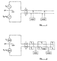
- an a.c. current distribution system embodying the present invention incorporates a conventional current source as previously described in relation to the current distribution system shown in Figure 2.
- the current source feeds the current loop comprising two conductive tracks 10,11.
- An impedance load L T is to be powered from the current loop.
- the load L T is split into two equal half loads L A, L B which are connected in series to respective tracks 10,11 substantially adjacent one another in the same locality - i.e. distance along the tracks from the current source.
- half the load L A is connected in series with the first track 10 and half the load L B is connected in series with the second track 11.
- the voltage on track 10 immediately before the first half load L A is V 1 and the voltage immediately after the first half load L A is V 1 -V LA .
- the voltage on track 11 immediately before the second half load L B is V 1 and the voltage immediately after the second half load L B on track 11 is V 1 -V LB .
- the current distribution system embodying the present invention maintains a substantially zero electric field not only along the tracks 10,11 before any impedance loads but also after any loads since the impedance loads are split evenly at substantially the same localities along the tracks 10,11 around the current loop.
- a load L T which can be split into equal parts as described above would be a double incandescent stop lamp comprising two separate 5 Ohm bulbs.
- the first bulb could comprise the first half load L A on the first track 10 and the second bulb of the pair could comprise the second half load L B on the track 11.
- two separate 5 Ohm bulbs could be connected to respective tracks 10,11 rather than using a single bulb. In this manner, the load is evenly split in the same locality between the tracks and the electric field along the tracks is thus maintained at substantially zero.
- the unsplitable load L T is connected to the terminals of a secondary winding S of a transformer.
- the transformer has a pair of primary windings P 1 , P 2 .
- One of the primary windings P 1 is connected in series with the track 10 and the other primary winding P 2 is connected in series at the same locality along the lengths of the tracks 10,11 to track 11.
- the primary windings are adjacent one another and are inductively coupled to the secondary winding S and thence to the load L T .
- P 1 and P 2 are substantially identical primary windings which cause identical voltage drops either side thereof such that the sum of the voltages at any locality along the track 10,11 within the distribution system at any one instant is zero. Accordingly, the electric field is maintained at substantially zero.
- Transformers which are used for other purposes such as isolation, voltage/current matching to a load or, indeed, control purposes can be easily integrated for use in an a.c. current distribution system embodying the present invention.
- Embodiments of the present invention are particularly well suited to operation at frequencies of the 20 kHz or greater range.
- the primary windings P 1 and P 2 have an identical number of turns and are perfectly matched and result in a 1:1 ratio with perfect coupling.
- the coupling between the primary windings is not perfect and can, therefore, lead to slight discrepancies between the voltages present immediately before the primary windings on the tracks 10,11 and those present immediately after the primary windings.
- a similar problem can arise if the load described in Figure 3 is not split exactly equally when connected in series on tracks 10 and 11.
- a balancing auxiliary transformer T x across the tracks 10,11.
- the auxiliary balancing transformer could be a tightly coupled bifilar wound toroid.
- the centre of the transformer coil is centre-tapped to zero volts. This arrangement serves to balance the voltages at the point of connection of the balancing transformer T x to the tracks 10,11 to be exactly opposite one another such that the sum of these voltages at the locality at any instant will be zero. Little power is transferred between the primary windings P 1 and P 2 so any current in the balancing transformers would be low.
- the existing primary and secondary windings P 1 , P 2 , S 1 , S 2 of an E-type core transformer connected to a load L T can be easily incorporated into an a.c. current distribution system according to the present invention by simply connecting the terminals of the first primary winding P 1 in series to track 10 and the terminals of the secondary primary winding P 2 in series to the track 11 at substantially the same locality along the tracks 10,11.
- the auxiliary balancing transformer T x can be implemented as shown in Figure 6.
- the balancing transformer T x has been wound around the central core of the E-type core. Respective pairs of primary and secondary windings P 1 , P 2 , S 1 , S 2 are wound in conventional positions on the other arms of the transformer.
- the central core of the transformer shown in Figure 6 can be wound with a control winding C to replace the balancing transformer T x .
- the primary windings P 1 , P 2 are split as previously described in relation to Figure 4 and connected respectively in series to the tracks 10,11 such that any voltage drop or phase shift across one primary winding is matched by one identical voltage drop or phase shift in the other primary winding. For example, for power lines or the like.
- the control winding When energised, the control winding saturates the core thereby limiting the voltage generated across the secondary windings S 1 , S 2 and provided to the inductance load L T . If the current to the control winding C around the saturable core is terminated, then the core becomes substantially un-saturated enabling the normal output voltage on the secondary windings S 1 , S 2 to power the load L T .
- Such an arrangement allows ready control and switching of the load by appropriately altering the current supplied to the control winding C, whilst maintaining an equal voltage drop across the primary windings connected in series to the respective tracks 10,11.
- the tracks 10,11 are made from copper and run parallel to one another and are spaced apart by a small distance in the order of 10ths of millimetres. These tracks 10,11 are separated by an insulating plastics layer 12 such as a polyester, polypropylene or polyphenylene sulphide. The thickness of the insulating layer 12 is in the order of 0.1mm.
Landscapes
- Engineering & Computer Science (AREA)
- Power Engineering (AREA)
- Supply And Distribution Of Alternating Current (AREA)
- Control Of Electrical Variables (AREA)
- Coils Of Transformers For General Uses (AREA)
Description
ΣV = V1 + V1 - VLoad. Further, at the tip of the loop, the sum of the voltages, ΣV, equals 2V1. The increase in the sum of the voltages, ΣV, from 0 to 2V1 results in a worsening electric field along the length of the track.
Claims (15)
- An a.c. current distribution system fed by a current source for providing electrical power to a load, the current distribution system comprising a first and a second conductive means (10, 11) which run parallel to one another, which are connectable, respectively, at one end to the current source and which are connected together at the other end to form a current loop, characterised in that the system includes coupling means to couple substantially one half of the load (LA) in series at a first position along the first conductive means (10) and to couple substantially the other half of the load (LB) in series at a second position along the second conductive means (11), the first and second positions being substantially adjacent one another.
- A system according to Claim 1, wherein the load comprises two distinct half loads (LA, LB), each of which is ohmically connected in series to the respective conductive means.
- A system according to Claim 1, wherein the load (LT) is inductively coupled to the respective conductive means by a transformer (Tx).
- A system according to Claim 3, wherein the load (LT) is ohmically connected across the terminals of one or more secondary windings (S1 S2) of the transformer (Tx)and the coupling means comprises a pair of substantially identical primary windings (P1 P2) of the transformer, each of which is ohmically connected in series to the respective conductive means (10,11), the voltage drops across the primary windings being substantially identical, such that the load is split substantially equally between the two primary windings.
- A system according to Claim 3 or 4, wherein the transformer (Tx) has an E-type core, the central core thereof being wound with a control coil operable to saturate the core to limit the voltage generated across the or each secondary winding.
- A system according to any preceding Claim, wherein a balancing transformer (Tx) centre-tapped to zero volts is connected across the first and second conductive means (10,11) to balance voltages on the conductive means at either end of the balancing transformer to be substantially opposite one another such that the sum of these voltages at any instant is zero.
- A system according to Claim 6, wherein the balancing transformer (Tx) is a tightly coupled bifilar wound toroid.
- A system according to Claim 6 or 7, wherein a balancing transformer (Tx) is incorporated in the current distribution system if the voltage drops across the means for coupling substantially one half of the load to the first conductive means and the other half of the load to the second conductive means are not substantially identical.
- A system according to any preceding Claims, wherein the conductive means (10,11) comprises a pair of conductive tracks.
- A system according to Claim 9, wherein the tracks (10,11) are made from copper.
- A system according to Claim 9 or 10, wherein the tracks (10,11) run parallel to one. another and are separated by an insulating material.
- A system according to Claim 11, wherein the insulating material is a plastics material such as polyester, polypropylene or polyphenylene sulphide.
- A system according to any preceding Claim, wherein the frequency of operation is in the region of 20 kHz or greater.
- A method of reducing the electric field in a current distribution system characterised in that the method comprises the steps of coupling a load to be powered by a current source feeding the current distribution system to a first and second conductive means (10,11) which run parallel to one another, which are connectable, respectively, at one end to the current source and which are connected together at the other end to form a current loop, wherein substantially one half of the load (LA) is coupled in series at a first position along the first conductive means and substantially the other half of the load (LB) is coupled in series at a second position along the second conductive means, the first and second positions being substantially adjacent one another such that the sum of the voltages on the conductive means in the same locality at any one instant is zero.
- A method according to Claim 14, wherein the load comprises two distinct half loads (LA, LB) which are ohmically connected in series to the respective conductive means.
Applications Claiming Priority (3)
| Application Number | Priority Date | Filing Date | Title |
|---|---|---|---|
| GB9701687 | 1997-01-28 | ||
| GBGB9701687.7A GB9701687D0 (en) | 1997-01-28 | 1997-01-28 | Improvements in or relating to an a.c. current distribution system |
| PCT/GB1998/000239 WO1998033256A1 (en) | 1997-01-28 | 1998-01-27 | An a.c. current distribution system |
Publications (2)
| Publication Number | Publication Date |
|---|---|
| EP0956629A1 EP0956629A1 (en) | 1999-11-17 |
| EP0956629B1 true EP0956629B1 (en) | 2002-01-09 |
Family
ID=10806679
Family Applications (1)
| Application Number | Title | Priority Date | Filing Date |
|---|---|---|---|
| EP98905118A Expired - Lifetime EP0956629B1 (en) | 1997-01-28 | 1998-01-27 | An a.c. current distribution system |
Country Status (5)
| Country | Link |
|---|---|
| US (1) | US6344699B1 (en) |
| EP (1) | EP0956629B1 (en) |
| DE (1) | DE69803440T2 (en) |
| GB (1) | GB9701687D0 (en) |
| WO (1) | WO1998033256A1 (en) |
Families Citing this family (20)
| Publication number | Priority date | Publication date | Assignee | Title |
|---|---|---|---|---|
| US6979959B2 (en) * | 2002-12-13 | 2005-12-27 | Microsemi Corporation | Apparatus and method for striking a fluorescent lamp |
| US7187139B2 (en) * | 2003-09-09 | 2007-03-06 | Microsemi Corporation | Split phase inverters for CCFL backlight system |
| US7183727B2 (en) * | 2003-09-23 | 2007-02-27 | Microsemi Corporation | Optical and temperature feedbacks to control display brightness |
| KR101085579B1 (en) * | 2003-10-06 | 2011-11-25 | 마이크로세미 코포레이션 | Current Sharing Method and Apparatus for Multiple CFC Lamp Operation |
| US7141933B2 (en) * | 2003-10-21 | 2006-11-28 | Microsemi Corporation | Systems and methods for a transformer configuration for driving multiple gas discharge tubes in parallel |
| WO2005059964A2 (en) | 2003-12-16 | 2005-06-30 | Microsemi Corporation | Current-mode driver |
| US7468722B2 (en) * | 2004-02-09 | 2008-12-23 | Microsemi Corporation | Method and apparatus to control display brightness with ambient light correction |
| WO2005099316A2 (en) * | 2004-04-01 | 2005-10-20 | Microsemi Corporation | Full-bridge and half-bridge compatible driver timing schedule for direct drive backlight system |
| US7250731B2 (en) * | 2004-04-07 | 2007-07-31 | Microsemi Corporation | Primary side current balancing scheme for multiple CCF lamp operation |
| US7755595B2 (en) | 2004-06-07 | 2010-07-13 | Microsemi Corporation | Dual-slope brightness control for transflective displays |
| US7061183B1 (en) | 2005-03-31 | 2006-06-13 | Microsemi Corporation | Zigzag topology for balancing current among paralleled gas discharge lamps |
| US7173382B2 (en) * | 2005-03-31 | 2007-02-06 | Microsemi Corporation | Nested balancing topology for balancing current among multiple lamps |
| US7414371B1 (en) | 2005-11-21 | 2008-08-19 | Microsemi Corporation | Voltage regulation loop with variable gain control for inverter circuit |
| US7569998B2 (en) | 2006-07-06 | 2009-08-04 | Microsemi Corporation | Striking and open lamp regulation for CCFL controller |
| TW200948201A (en) | 2008-02-05 | 2009-11-16 | Microsemi Corp | Arrangement suitable for driving floating CCFL based backlight |
| US8093839B2 (en) * | 2008-11-20 | 2012-01-10 | Microsemi Corporation | Method and apparatus for driving CCFL at low burst duty cycle rates |
| US9030119B2 (en) | 2010-07-19 | 2015-05-12 | Microsemi Corporation | LED string driver arrangement with non-dissipative current balancer |
| WO2012151170A1 (en) | 2011-05-03 | 2012-11-08 | Microsemi Corporation | High efficiency led driving method |
| US8754581B2 (en) | 2011-05-03 | 2014-06-17 | Microsemi Corporation | High efficiency LED driving method for odd number of LED strings |
| US9554444B2 (en) | 2012-12-17 | 2017-01-24 | OV20 Systems | Device and method for retrofitting or converting or adapting series circuits |
Family Cites Families (8)
| Publication number | Priority date | Publication date | Assignee | Title |
|---|---|---|---|---|
| US390990A (en) * | 1888-10-09 | System of electrical distribution | ||
| US3783374A (en) | 1972-04-07 | 1974-01-01 | Sundstrand Data Control | Capacitance difference detector circuit |
| US4772806A (en) * | 1987-05-01 | 1988-09-20 | Shay Lean | Switching device for a series loop circuit |
| US4912372A (en) * | 1988-11-28 | 1990-03-27 | Multi Electric Mfg. Co. | Power circuit for series connected loads |
| EP0587923A1 (en) * | 1992-09-14 | 1994-03-23 | U.R.D. Co. Ltd. | High-frequency constant-current feeding system |
| US5394065A (en) * | 1992-11-09 | 1995-02-28 | Tunewell Technology Limited | Circuit for supplying current to a discharge tube |
| GB9304132D0 (en) | 1993-03-01 | 1993-04-14 | Tunewell Transformers Ltd | Improvements in or relating to an electrical arrangement |
| US5886423A (en) * | 1997-09-10 | 1999-03-23 | Leviton Manufacturing Co., Inc. | Electric series circuit |
-
1997
- 1997-01-28 GB GBGB9701687.7A patent/GB9701687D0/en active Pending
-
1998
- 1998-01-27 EP EP98905118A patent/EP0956629B1/en not_active Expired - Lifetime
- 1998-01-27 WO PCT/GB1998/000239 patent/WO1998033256A1/en not_active Ceased
- 1998-01-27 DE DE69803440T patent/DE69803440T2/en not_active Expired - Fee Related
- 1998-01-27 US US09/355,428 patent/US6344699B1/en not_active Expired - Fee Related
Also Published As
| Publication number | Publication date |
|---|---|
| DE69803440T2 (en) | 2002-08-29 |
| GB9701687D0 (en) | 1997-03-19 |
| EP0956629A1 (en) | 1999-11-17 |
| US6344699B1 (en) | 2002-02-05 |
| DE69803440D1 (en) | 2002-02-28 |
| WO1998033256A1 (en) | 1998-07-30 |
Similar Documents
| Publication | Publication Date | Title |
|---|---|---|
| US6344699B1 (en) | A.C. current distribution system | |
| US11251713B2 (en) | Multiple parallel-connected resonant converter, inductor-integrated magnetic element and transformer-integrated magnetic element | |
| US4473811A (en) | Single bobbin transformer having multiple delink windings and method of making same | |
| US6686823B2 (en) | Inductive power transmission and distribution apparatus using a coaxial transformer | |
| US4943763A (en) | Ferroresonant transformer with dual outputs | |
| JP2835340B2 (en) | Voltage generator | |
| IE872902L (en) | Electronic equipment for control of fluorescent lamps | |
| US20040217826A1 (en) | Network coupler | |
| US4254459A (en) | Direct current to direct current converter | |
| JPH0487570A (en) | High-frequency inverter | |
| US4500829A (en) | Advance and retard phase-shift transformer | |
| Zhu et al. | Wireless power transformation for data centers and medium voltage applications | |
| CN1845267B (en) | Transformer and discharge lamp lighting device | |
| US20010026463A1 (en) | Arrangement for transferring information in transformer | |
| US4159457A (en) | Low voltage high current transformer | |
| US4177509A (en) | Self-excited inverter with suppressed current spikes | |
| US4194128A (en) | Ripple control systems | |
| CN109952623A (en) | Low common-mode noise transformer device structure with external floating line supporting plate | |
| US6426610B1 (en) | Controlled ferroresonant constant current source | |
| US20050018452A1 (en) | Contactless power supply | |
| US20110080055A1 (en) | Magnetically Integrated Current Reactor | |
| US4378522A (en) | Adjustable current source | |
| US4532582A (en) | Voltage regulator system using magnetic controllers | |
| US3585493A (en) | Voltage-regulating device | |
| US3904954A (en) | Voltage regulating transformer for series coupled loads |
Legal Events
| Date | Code | Title | Description |
|---|---|---|---|
| PUAI | Public reference made under article 153(3) epc to a published international application that has entered the european phase |
Free format text: ORIGINAL CODE: 0009012 |
|
| 17P | Request for examination filed |
Effective date: 19990827 |
|
| AK | Designated contracting states |
Kind code of ref document: A1 Designated state(s): DE FR GB IT |
|
| 17Q | First examination report despatched |
Effective date: 20000821 |
|
| GRAG | Despatch of communication of intention to grant |
Free format text: ORIGINAL CODE: EPIDOS AGRA |
|
| GRAG | Despatch of communication of intention to grant |
Free format text: ORIGINAL CODE: EPIDOS AGRA |
|
| GRAH | Despatch of communication of intention to grant a patent |
Free format text: ORIGINAL CODE: EPIDOS IGRA |
|
| GRAH | Despatch of communication of intention to grant a patent |
Free format text: ORIGINAL CODE: EPIDOS IGRA |
|
| GRAA | (expected) grant |
Free format text: ORIGINAL CODE: 0009210 |
|
| REG | Reference to a national code |
Ref country code: GB Ref legal event code: IF02 |
|
| AK | Designated contracting states |
Kind code of ref document: B1 Designated state(s): DE FR GB IT |
|
| PGFP | Annual fee paid to national office [announced via postgrant information from national office to epo] |
Ref country code: GB Payment date: 20020206 Year of fee payment: 5 |
|
| PGFP | Annual fee paid to national office [announced via postgrant information from national office to epo] |
Ref country code: FR Payment date: 20020212 Year of fee payment: 5 |
|
| PGFP | Annual fee paid to national office [announced via postgrant information from national office to epo] |
Ref country code: DE Payment date: 20020227 Year of fee payment: 5 |
|
| REF | Corresponds to: |
Ref document number: 69803440 Country of ref document: DE Date of ref document: 20020228 |
|
| ET | Fr: translation filed | ||
| PLBE | No opposition filed within time limit |
Free format text: ORIGINAL CODE: 0009261 |
|
| STAA | Information on the status of an ep patent application or granted ep patent |
Free format text: STATUS: NO OPPOSITION FILED WITHIN TIME LIMIT |
|
| 26N | No opposition filed | ||
| PG25 | Lapsed in a contracting state [announced via postgrant information from national office to epo] |
Ref country code: GB Free format text: LAPSE BECAUSE OF NON-PAYMENT OF DUE FEES Effective date: 20030127 |
|
| PG25 | Lapsed in a contracting state [announced via postgrant information from national office to epo] |
Ref country code: DE Free format text: LAPSE BECAUSE OF NON-PAYMENT OF DUE FEES Effective date: 20030801 |
|
| GBPC | Gb: european patent ceased through non-payment of renewal fee | ||
| PG25 | Lapsed in a contracting state [announced via postgrant information from national office to epo] |
Ref country code: FR Free format text: LAPSE BECAUSE OF NON-PAYMENT OF DUE FEES Effective date: 20030930 |
|
| REG | Reference to a national code |
Ref country code: FR Ref legal event code: ST |
|
| PG25 | Lapsed in a contracting state [announced via postgrant information from national office to epo] |
Ref country code: IT Free format text: LAPSE BECAUSE OF NON-PAYMENT OF DUE FEES Effective date: 20050127 |